Note: Descriptions are shown in the official language in which they were submitted.
CA 02354327 2001-07-30
TRANSPORT INTERFACE FOR TIME DIVISION FRAMES
INCORPORATION BY REFERENCE OF PRIORITY DOCUMENT
This application is based on and claims the benefit of Italian Patent
Application
No. TO 2000A 000 760, filed JULY 31, 2000, which is incorporated by
reference herein.
s BACKGROUND OF THE INVENTION
1. Field Of The Invention
The present invention relates to a transport interface for time division
frames, in particular SDH frames, and related interfacing method of time
division
frames.
l0 2. Description Of The Prior Art
In modern digital communication systems, the various information streams,
or data, propagating on telecommunication networks are multiplexed in frames
according to predetermined transport protocols, such as SDH (Synchronous
Digital Hierarchy) transport protocol for time division frames. This transport
15 protocol is particularly suitable tar conveying and distributing the
numerous
information streams among the various telecommunications network nodes.
Therefore, various logic circuits are arranged inside the
telecommunications network nodes, such as SDH network, apt to process in
different ways the time division frame received from the node. These
operations
ao are essentially related to dealing with the synchronism and with the
extraction of
the various data streams multiplexed inside the time division frame, as well
as
1
CA 02354327 2001-07-30
with the subsequent processing of the various information streams extracted
from
said time division frames.
Therefore, in order to process the SDH time division frame, an ASIC
(Application Specific Integrated Circuit) circuit, i.e. a dedicated circuit is
s developed, which performs SDH operations on the frame by extracting and
inserting the information streams, also called tributaries, from the so called
Virtual
Containers, wherein they are multiplexed. This ASIC circuit can be followed by
FPGA (Field Programmable Gate Arrays) circuits, i.e. circuits adaptable
according
to their utilization and located outside the ASIC circuit, which process the
1o tributaries extracted from the frame, such as processing the streams that
use
ATM (Asynchronous Transfer Mode) protocol or lP (Internet Protocol) protocol,
previously multiplexed inside the SDH frame. Due to their flexibility, FPGA
circuits
are frequently employed in conjunction with dedicated circuits.
Communications between AS1C circuits and related FPGA circuits are
usually defined as 'intra-equipment' communications, namely communications
occurring inside the telecommunications network node, whereas communications
between the nodes are called line communications. The same interface protocols
employed for the nodes receiver interfaces are also used for the above intra-
equipment communications of tributaries, such as the so called Network Node
ao Interfaces, i.e. network node interfaces for line communications to other
nodes.
This causes some drawbacks, since the tributaries are sent to FPGA
devices under a very complex structure defined by SDH protocol, which is
redundant compared with the needs, and requires the use of complex interfaces
2
CA 02354327 2001-07-30
between the FPGA devices and ASIC circuit.
Moreover, the interfaces of the ASIC circuit are not flexible, since they have
to operate on different protocols, i.e. ATM or IP, which are not structure
compatible. For instance, an ASIC circuit can communicate with a certain
number
s of FPGA devices performing certain termination functions, e.g. operating
according to ATM protocol, but cannot communicate with FPGA devices using IP
protocol, unless they have further transport interfaces expressly provided for
handling IP protocol available. This reduces ASIC circuit flexibility.
SUMMARY OF THE INVENTION
It is the object of the present invention to solve the above drawbacks and
provide a transport interface for time division frames, in particular SDH
frames,
andlor an interfacing method of time division frames, having a more efficient
and
improved performance with respect to existing solutions.
In this framework, it is the main object of the present invention to provide a
transport interface for time division frames, in particular SDH frames, which
has a
lower complexity with respect to existing solution.
A further object of the present invention is to provide a transport interface
for time division frames, in particular SDH frames, which is flexible and can
be
utilized by any circuits implementing various termination functions.
ao In order to achieve such objects, it is the subject of the present
invention to
provide a transport interface for time division frames, in particular SDH
frames,
and/or an interfacing method of time division frames, incorporating the
features of
the annexed claims, which form an integral part of the description herein.
J
CA 02354327 2001-07-30
It is a particular subject of the present invention a transport interface for
time division frames, in particular SDE-I frames, being transmitted between
network
nodes according to a specified transport protocol, said nodes comprising first
circuit means for processing said time division frames according to said
specified
s transport protocol, and second circuit means for exchanging second
information
streams with said first circuit means through said transport interface,
wherein said
transport interface provides for structuring said second information streams
as a
data stream, sent in a co-directional way, and an address information.
It is a further particular subject of the present invention a method for
interfacing
to time division frames, in particular SDH frames, which provides for
extraction and
exchange of the data streams multiplexed in said time division frames between
a
time division frame processing circuit and devices for processing the data
streams
contained in said time division frames, wherein it provides for the step of
allocating
a data stream and an address information, for co-directional information
exchange
between the time division frame processing circuit and the processing devices.
BRIEF DESCRIPTION OF THE DRAWINGS
Further objects, features and advantages of the present invention will become
apparent from the following detailed description and annexed drawings, which
are
supplied by way of non limifiing example, wherein:
zo - Fig. 7 shows a block diagram of a transport interface for time division
frames,
in particular SDH frames, according to the present invention;
Fig. 2 shows a more detailed block diagram of the transport intertace for time
division frames, in particular SDH frames, of Figure 1.
4
between the FPGA devices
CA 02354327 2001-07-30
BEST MODE FOR CARRYING OUT THE INVENTION
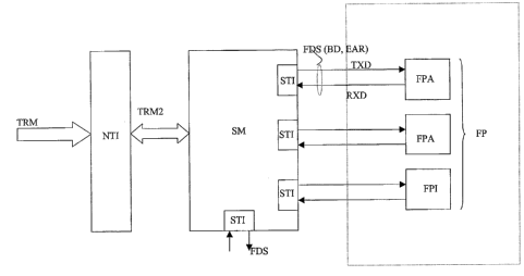
Figure 1 is representing a basic diagram of the architecture of a
telecommunications network, wherein the transport interface according to the
present invention is operating.
s This figure shows a time division frames stream TRM structured according to
the SDH protocol, said frames stream TRM being received by a network interface
of the node NTI that transmits to the main board of a switch matrix SM,
sending a
frames streamTRM2 adapted for said switch matrix SM. This switch matrix SM is
obtained through an ASIC circuit and extracts for instance the tributaries
from the
to frames stream TRM and processes their addresses.
The switch matrix SM communicates with a plurality of devices foi- processing
the tributaries FP, external to the ASIC circuit and implemented by FPGA
circuits,
which perform the processing of the tributaries extracted from the switch
matrix
SM.
i5 In the instance of Figure 1, there are indicated by way of example two
devices
FPA for processing the tributaries according to the ATM protocol and a device
FPl
for processing the tributaries according to the Internet Protocol.
According to the present invention, the switch matrix SM is equipped with
appropriate transport interfaces STI, which exchange a special data stream FDS
ao with the devices for processing the tributaries FP. Said special data
stream FDS,
the structure of which will be better detailed with reference to Figure 2,
comprises
anyway a transmitted stream TXD, received by the device FP, and a received
stream RXD, transmitted by the device FP and requested by the transport
CA 02354327 2001-07-30
interface STI.
The basic inventive idea of the transport interface STI consists in that a
data
stream FDS contains a data bus BD, sent in a co-directional mode in both
directions, wherein the information contents of the tributary to be processed
is
s conveyed, and a minimum set of signals, i.e. an auxiliary signal EAR
accompanying the data bus BD, comprising enable information and identifying
information of the payload, i.e. an address of the tributary or port wherefrom
it is
extracted.
Thus, the device for processing the tributaries FP is only receiving data,
~o information about the validity of said data through the enable information,
and
address information to allocate the tributary inside it. Vice-versa, the
transport
interface STI according to the present invention will receive the data bus BD
from
the device for processing the tributaries FP sending the auxiliary signal EAR
in the
form of a request, i.e. the address information identifies the tributary
requested by
the transport interface STI, whereas the enable information will act as a
request to
send the payload.
In Figure 2 the transport interface STI of the switch matrix SM is shown,
consisting of a receiver RXTi and transmitter TXTI. The transmitter TXTI
receives
at its input a plurality of Arbitrary Units AUO, AU1, AU2, AU3, which have
been
ao extracted inside the switch matrix SM from a frame TRM, and containing
Tributary
Unit tributaries, whose payload has to be sent in the transmitted stream TXD
to
the transport interface STI of the device for processing the tributaries FP.
As shown in Figure 2, according to known demapping procedures the pointers
6
CA 02354327 2001-07-30
related to the AU and TU structures are taken out of the four Arbitrary Units
AUO,
AU1, AU2, AU3 through appropriate logic circuits PI, called Pointer
Interpreters,
and the Arbitrary Units are multiplexed at a quadruple frequency in a data bus
T_BD by a suitable multiplexes BM also generating an auxiliary signal T-EAR.
s Figure 2 also shows a desynchronizing circuit DS, which according to known
techniques drives the multiplexes BM to generate plesiochronous streams (no
longer synchronous as inside the switch matrix SM).
The receiver RXTI receives the transmitted data over a data bus R BD and
demultiplexes them at a lower frequency, through a demultiplexer DM, to a
first
insertion block BI controlled by a time base BT, which also controls the
generation
through a multiplexes MX of an auxiliary signai R EAR, which requests the data
to
be mapped in the Virtual Containers of the frames TRM from the device for
processing the tributaries FP. A synchronizing circuit SD is also provided,
which
controls, according to known mapping techniques, the flow of the data streams
15 from the plesiochronous edge, represented by the data bus R_BD outside the
transport interface STI, to the synchronous edge in the switch matrix SM. The
synchronizing circuit SD supplies the timing to a multiplexes MX2, which
receives
the demultiplexed data streams from the insertion block BI and inserts them in
the
Arbitrary Units A0, A1, A2, A3, to be subsequently multiplexed.
ao The signal in the data bus BD, either received or transmitted by the
interface
STI, is an 8-bit signal either containing the payload of the tributary element
extracted from the Virtual Container, in the case it belongs to the
transmitted
stream TXD, i.e. it is the data bus T_BD, or containing the payload to be
inserted
7
CA 02354327 2001-07-30
in a Virtual Container in the case it belongs to the received stream RXD, i.e.
the
data bus R BD.
As explained above, the interface STI generates the auxiliary signal EAR,
which corresponds to the above minimum set of signals required for the
handling
s of the data bus BD by the device for processing the tributaries FP.
The auxiliary signal TEAR is actually a 9-bit signal: the bits 0 to 5 contain
an
address information of the tributaries being extracted, the bits 6 and 7
contain
information about the Arbitrary Unit AU being extracted, the bit 8 is an
enable bit,
i.e. if it is at logic one, the data is valid for the receiver of the
transport interface
STI. The data bus T DB and the auxiliary signal T EAR form the transmitted
stream TXD, which is received exactly from the device for processing the
tributaries FP.
The received stream RXD, flowing from the processing device FP to the switch
matrix SM, is substantially sent in reply to a data request signal issued by
the
is transport interface STI, as mentioned above. In this case, it is the
auxiliary signal
REAR, wherein also the first 6 bits (0 to 5) contain information about the
requested tributaries, bits 6 and 7 contain information about the requested
Arbitrary Unit AU, whereas the bit 8 is a request enable bit.
The tributaries processing device transmits the requested tributary to the
data
ao bus R_BD through the auxiliary signal R EAR, to be mapped into an SDH
Virtual
Container by means of the switch matrix SM receiving it.
Consequently, if the transport interface STI requests to insert a payload
(which
will be transmitted to it through the data bus R_BD) in the tributary 0, AU=0,
the
8
CA 02354327 2001-07-30
auxiliary signal R EAR will substantially have the following binary contents:
R_EAR(8:0)="1 "&"00"& "00000"
According to a feature of the present invention, the device for processing the
tributaries FP supplies the data to be inserted, conveyed in the data bus BD,
with
s a delay with respect to the auxiliary signal EAR. This delay can be set at a
predetermined number of clock intervals, which can be reset, as per FPGA
circuit
requirements. In the event of a 77MHz operating frequency, this delay is 7
clock
shots.
The signals described in the above examples have a minimum configuration
and are suitable for general protocols, such as Internet Protocol. In the
event of
tributaries exchange with the tributaries processing device FPA, operating
according to the Asynchronous Transfer Mode protocol, a 1-bit synchronism
signal, utilized by the tributaries processing device FPA for marking the
start of
the ATM cells, as well as an alarm bit TSF for the device for processing
tributaries
FPA, can be sent into the transmitted stream TXD, besides the auxiliary signal
T EAR. In this event, additional pins for these signals can be provided.
This synchronism signal can be alternatively used for marking a particular bit
of
the transport protocol or of the payload, such as in the case of Gbit
Ethernet.
In the event of ATM protocol, the received stream RXD will equally contain in
ao addition a synchronism bit, for the switch matrix SM, pointing to the
correct bit of
payload start, or a specific byte for the correct mapping in the ASIC.
From the above description the features of the present invention are clear,
and
also its advantages are clear.
9
CA 02354327 2001-07-30
The transport interface for time division frames, in particular SDH frames
according to the present invention will advantageously make intra-equipment
communication easier between the switch matrix or other central circuits for
time
division frames, and the peripheral frame processing devices. This will also
s simplify the control logic requested for processing information streams,
i.e.
reducing interface complexity.
Moreover, the transport interface for time division frames, in particular SDH
frames according to the present invention will advantageously increase ASIC
circuit flexibility when in use with FPGA circuits; also in the case of the
circuit
~o having dedicated interfaces for special protocols, it can always be
equipped with a
transport interface covered by the present invention, so as to be able to take
tributaries at any time according to a simple adaptable protocol and increase
its
flexibility.
There has thus been shown and described a novel transport interface for
i5 time division frames, in particular SDH frames, and a novel interfacing
method of
time division frames, which fulfill all the objects and advantages sought
therefor.
Many changes, modifications, variations and other uses and applications of the
subject invention will, however, become apparent to those skilled in the art
after
considering the specification and the accompanying drawings which disclose
ao preferred embodiments thereof. All such changes, modifications, variations
and
other uses and applications which do not depart from the spirit and scope of
the
invention are deemed to be covered by the invention which is limited only by
the
claims which follow.
CA 02354327 2001-07-30
In particular, the time division data frames on which the interface according
to the present invention operates may have different formats.
11