Note: Descriptions are shown in the official language in which they were submitted.
CA 02354473 2001-06-13
Patent-Treuhand-Gesellschaft
fur elektrische Gliihlampen mbH, Munich
Drive circuit for 7~EDs and an associated operating
method
The present application hereby expressly refers to the
German Application DE-A 199 30 174.3, which has not yet
been published.
The invention is based on a drive circuit for LEDs and
an associated operating method as claimed in the
preamble of claim 1. This relates in particular to
reducing the drive power losses in light-emitting
diodes (LEDs) by means of a pulsed LED drive circuit.
As a rule, series resistors are used for current
Limiting when driving light-emitting diodes (LEDs),
see, for example, US-A 5 907 569. A typical voltage
drop. across light-emitting diodes (UF) is a few volts
(for example, for Power TOPLED OF - 2.1 V). The known
resistor R" in series with the LED (see figure 1 in
DE-A 19930174.3) produces a particularly high power
loss, particularly if the battery voltage UBatt is
subject to major voltage fluctuations (as is normal in
motor vehicles). The voltage drop across the LED still
remains constant even when such voltage fluctuations
occur, that is to say the residual voltage across the
series resistor R~ falls. R" is thus alternately loaded
to a greater or lesser extent. In practice, a number of
LEDs are generally connected in series (cluster) in
order to achieve better drive efficiency (figure 2 in
DE-A 19930174.3). Depending on the vehicle power supply
system (12 V or 42 V), an appropriate number of LEDs
can be combined to form a cluster . With a 12 V vehicle
power supply system, there is a lower limit on the
battery voltage UBatt down to which legally specified
safety devices (for example the hazard~warning system)
must be functional. This is 9 volts. This means that,
CA 02354473 2001-06-13
-
in this case, up to 4 Power TOPLEDs can be combined to
form a cluster (4 x 2.1 V = 8.4 V).
Furthermore, DE-A 19930174.3 describes the use of a
pulsed LED drive to reduce the drivepower loss in
light-emitting diodes (LEDs). When the LEDs are driven
in this way, the current is regulated autonomously in
each individual LED cluster: This leads to the maximum
possible reliability (intelligent LED driver module,
see figure 4 in DE-A 199 30 174.3). However, a
relatively large number of LED driver modules are
required to illuminate a relatively large area - as is
the case with motor vehicle tail lights - using this
technique, and this results in considerable costs. The
number of LED driver modules depends on two factors:
The smaller the available supply voltage U" for the LED
cluster, the greater is the number of clusters
required.
The greater the forward voltage drop OF across the LEDs
which are intended to be used for an LED cluster, the
smaller is the number of LEDs which can be used in one
cluster.
The greater the number of LED driver modules required,
the greater are the costs.
The requirements to which an LED drive as described in
DE-A 19930174.3 is subject are, of course, complied
with, for example temperature regulation and fault
identification are possible in the LED cluster.
One object of the present invention is to provide a
drive circuit for LEDs as claimed in the preamble of
claim 1, which is simpler and thus considerably more
cost-effective.
CA 02354473 2001-06-13
- 3 -
This object is achieved by the distinguishing features
of claim 1. Particularly advantageous refinements can
be found in the dependent claims.
The fundamental principle of the present invention is
to cascade the already known drive system. An LED drive
based on the concept in DE-A 19930174.3 is simplified
in that the basic drive clock is governed by the clock
(CLK) of the transistor T1 in a first higher-level LED
cluster, which is referred to as the '.'master" in the
following text, at the output of the comparator of the
associated control loop, and this clock is also made
available to other lower-level LED clusters (slaves)
(figure 1) . The resistors Rssn connected in series with
the LEDs represent optional additional shunt resistors
Rsnunt- These are not absolutely essential in operation,
since their values are chosen to be very small (for
example, Rssi = ls2) and they do not adversely affect the
setting of the forward current IF. However, if
interruption identification is intended to be carried
out in the slave clusters (see below) they are
essential.
This concept in principle allows an area of any desired
size to be illuminated using a single control loop.
This is so-called master/slave current regulation, with
the master cluster predetermining the clock (CLK) and
all the additional LED clusters (slave clusters) being
driven by the master clock:
In the simplest embodiment, only one master cluster is
used. This solution is particularly cost-effective.
However, in this case, it is advantageous to ensure
that the number of LEDs in the slave clusters is the
same as the number in the single master cluster.
Otherwise, brightness and light intensity differences
would occur.
CA 02354473 2001-06-13
- 4 -
In one particularly preferred embodiment, the number of
LEDs in the clusters can be varied. In this case, there
are two different embodiments for driving the LED
clusters which have different numbers of LEDs (for
example if the number of LEDs in the master cluster is
greater):
In a first variant, a series load (resistor, zener
diode or the like), in particular a series resistor RXn.
is connected in each n-th slave cluster, replacing the
missing light-emitting diode (or light-emitting
diodes). In this case, the master clock is the drive
clock of that LED cluster which is driving the greatest
number of light-emitting diodes (figure 2). The number
of LEDs in the other clusters (slave clusters) may in
this case be chosen to be the same, or less. It is
advantageously not more than 30$ less than the number
in the master cluster, in order to avoid the losses
becoming too large.
In a second variant, one or more additional LED control
loops (second or third, etc: master control loop) is or
are integrated in the LED drive module (IC) , whose LED
cluster operates with a smaller number of LEDs than the
first master cluster. The battery voltage UBatt .is in
this case connected to all the transistors T. The drive
clock of the second master control loop (CLK2) is then
made available to the group of slave clusters having
the corresponding, lesser number of LEDs (figure 3).
This embodiment is suitable for groups of LED clusters
which each have the same number of LEDs.
The failure rate of a master cluster is preferably also
improved. This is because the master clock is no longer
available to any of the connected slaves if the master
fails, for whatever reason (for example interruption).
The slaves are no longer driven, and must then likewise
be switched off to protect them against~destruction.
CA 02354473 2001-06-13
- 5 -
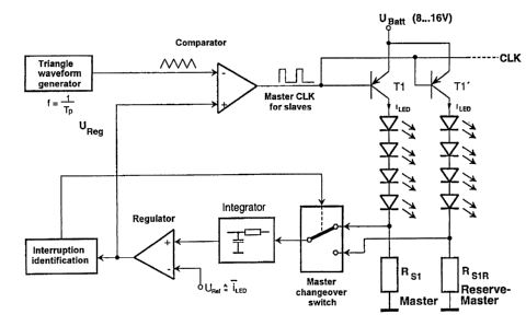
One of the slave clusters is thus advantageously in the
form of a reserve master cluster. This means that a
means is provided for identifying an interruption in
the control loop of the master cluster and this means,
for its part, is connected to a changeover switch in
the control loop, with the changeover switch being
connected on the one hand to the master cluster and on
the other hand to the reserve master cluster. If the
master fails, the switch is then changed to the reserve
master cluster (figure 4). This redundancy ensures
that, if the master is operating incorrectly
(interruption), an immediate change is made to the
reserve master. This ensures that the connected slaves
(not shown) continue to receive their drive clock
(master clock) for operation.
The reserve master is preferably used as a slave as
long as the master 1 is operating normally.
Fault identification (malfunction) in the LED cluster
is also preferably improved. The commonest fault types
are interruptions and short-circuits. An LED failure
always means an interruption. In this case, this means
an interruption in the LED cluster, that is to say at
least one LED has failed.
Nevertheless, it is possible for a short-circuit to
occur, to be precise in the sense of an interruption in
the electrical connecting line between the LED anode
(A1) and ground (GND), see figure 5. Especially for use
in motor vehicles (for example a tail light composed of
LEDs), this type of fault must be detected so that
appropriate countermeasures can be initiated in the
event of a fault, such as immediately switching off the
LED driver module or switching off only the short-
circuited load circuit (LED cluster). The "short-
circuit" fault type can be caused, for example, by a
rear impact in which the tail light is damaged.
CA 02354473 2001-06-13
- 6 -
Fault identification in all the clusters is thus highly
recommended. For this purpose, detector inputs for the
slave clusters are required in the driver module (IC),
to be precise preferably a first input for interruption
identification (figure 5, OL) and a second input for
short-circuit identification (SC in figure 5). OL
stands for "open load" (interruption), while SC stands
for short circuit.
The total number of detector inputs is governed by the
number of slave clusters which are intended to be
monitored. Normally, two module inputs are required per
slave cluster.
The fundamental elements of an LED drive circuit are
described~in DE-A 199 30 174.3. Now, as shown in figure
5, elements are added for operation based on the
master-slave method. For completeness, all of these are
quoted here:
constant-current regulation of the forward current
(IF = constant) for the LEDs
external, and thus flexible, forward-current adjustment
low power loss due to switched operation (no need for
the large series resistor R")
interruption identification in the LED cluster
short-circuit identification on the LED cluster
temperature regulation in order to protect the LEDs
flexibility in driving different numbers of LEDs in the
clusters, by means of a second LED master control loop
CA 02354473 2001-06-13
-
drive clock output (clock output) from the master 1 and
the master 2 for the associated slave clusters with
equal numbers of LEDs
increase in reliability by master switching
logic drive (microcontroller-compatible ENABLE input)
low intrinsic. current draw by the drive circuit in
operation and in the standby mode
resistant to polarity reversal (integrated in the IC,
or can be provided externally by connector coding)
overvoltage protection
compact housing (for example Power SO housing for SMD
technology)
temperature range -40°C < Tj <_ 150°C
42 V motor vehicle power supply system (also feasible
for 12 V motor vehicle power supply system).
Figures
The invention will be explained in more detail in the
following text with reference to a number of exemplary
embodiments. In the figures:
Figure 1 shows the basic principle of pulsed
current regulation for LEDs based on the
master-slave principle
Figure 2 shows a further exemplary embodiment of
a drive circuit with different numbers
of LEDs in the individual clusters
CA 02354473 2001-06-13
Figure 3 shows a further exemplary embodiment of
a drive circuit having two master
clusters
Figure 4 shows a further exemplary embodiment of
a drive circuit having a reserve master
cluster
Figure 5 shows a basic block diagram of. an .LED
drive circuit of pulsed current
regulation for LEDs
Figure 6 shows an LED drive circuit without fault
identification
Figure 7 shows an LED drive circuit with complete
fault identification.
Description of the drawings
Figures 1 to 5 have already been described above.
The schematic application circuit in figure 6 is
illustrated without fault identification for the slave
clusters. Details are illustrated in figure 8 of
DE-A 199 30 174.3. The slave clusters are controlled in
groups by the associated, regulated master cluster. In
the situation where fault identification can be
-dispensed with in a particular application, the
detector input or inputs (OL and SC) of the slave
clusters must be connected to a fixed potential (for
example HIGH).
This different to the situation shown in figure 7. In
this case, the detector inputs OL and SC are also used
for fault identification in the slave clusters.