Note: Descriptions are shown in the official language in which they were submitted.
CA 02355084 2001-06-13
WO 00/36390 PCT/US99/29741
MICROFLUIDIC CIRCUIT DESIGNS FOR PERFORMING
ELECTROKINETIC MANIPULATIONS THAT REDUCE
THE NUMBER OF VOLTAGE SOURCES AND FLUID RESERVOIRS
FIELD OF THE INVENTION
The invention relates to a microchip design for the electrokinetic
manipulation of chemical and biological materials. More specifically, this
invention relates to a microchip device in which the reagent and mixing
channels
are dimensioned to proportion the electrokinetic driving forces without the
need
for external voltage division schemes or multiple independent power supplies,
and to reduce the number of fluidic reservoirs needed for operability,
relative to
known microchip devices. Similar advantages are provided by embodiments for
performing dispensing operations.
BACKGROUND OF THE INVENTION
The mixing of two or more liquid-phase materials or the dispensing of a
reagent material on a microchip is accomplished by controlling the electric
potentials applied to the various reservoirs to electrokinetically drive the
materials housed therein through the channels of the microchip. Heretofore,
this
process has required external voltage control means such as a power supply
employing a voltage divider network, or programmable power supplies. Such
external voltage sources are utilized to effect valuing and mixing phenomena
in
the channel manifold of a microfabricated device.
Because of the configurations of the known voltage sources it has been
necessary to use a plurality of voltage source leads and corresponding
microchip
contact points in order to apply the multiple electric potentials. The number
of
such sources and accompanying hardware to effect electrokinetic phenomena can
be quite bulky and require complex architectures to control. This is most
evident
-1-
CA 02355084 2001-06-13
WO 00/36390 PCTNS99/29741
in highly parallel architectures, especially if each node requires a different
applied
potential from an external source.
Therefore, a need has arisen for a microchip that is capable of mixing
sample material in various proportions and dispensing variable volumes of a
sample material in which the fluid material is driven electrokinetically by a
single
high voltage supply. In this way, excess wires and circuitry needed for a
voltage
division scheme or the complexity of multiple programmable power supplies can
be eliminated and the microchip can be implemented with fewer fluidic
reservoirs
compared to the known designs.
SUMMARY OF THE INVENTION
The present invention provides a microfabricated device for liquid phase
chenucal and biological analysis. A device in accordance with the invention
includes a substrate on which a series of microchannels are formed. A cover
15 plate is bonded to the substrate to close the open side of the
microchannels.
Reservoirs are in fluidic communication with the end of the microchannels. The
reservoirs are in electrical contact with a high voltage power source
providing
electrical potential for electrokinetically mixing and/or dispensing fluidic
materials contained therein.
The microchip includes a series of tributary channel junctions ( "tees"
and/or four-way intersections) wherein at least two tributary reagent
microchannels communicate with a common mixing microchannel. The tributary
reagent channels have either different cross sectional areas, different
lengths, or
both and, therefore different electrical resistances. The material in the
tributary
reagent channels is mixed at a channel junction depending on the ratio of the
channel electrical resistances. Such an approach can handle all or a portion
of the
voltage division on the microchip without using techniques external to the
microchip. The mixing of two or more materials is achieved using
electrophoretic and/or electroosmotic transport. In accordance with another
-2-
CA 02355084 2001-06-13
WO 00/36390 PCTNS99/29741
aspect of the present invention, there is provided a microfabricated device
that is
capable of dispensing variable volumes of a sample material. In accordance
with
a further aspect of this invention, the tributary channels are formed so that
a
reduced number of material reservoirs can be utilized when performing multiple
ratio assays or reactions.
A first category of microfabricated devices in accordance with the present
invention provides a voltage division technique that utilizes a reduced number
of
different external voltage sources to effect nucrofluidic reagent mixing
relative to
previous devices. A second category of microfabricated devices in accordance
with this invention allows dispensing of samples on a mufti-port device with a
single external high voltage supply and switch.
BRIEF DESCRIPTION OF THE DRAWINGS
The foregoing summary, and the following detailed description, will be
best understood when read in conjunction with the attached drawings, in which:
Figure 1 is a schematic diagram showing a mixing junction in accordance
with this invention;
Figure 2 is a schematic diagram of a fluidic microchip for mixing
reagents in accordance with the present invention;
Figure 2a is a schematic diagram of an alternative embodiment of the
fluidic microchip shown in Figure 2;
Figure 3 is a graph of the average fluorescence signals in the waste
channels of the fluidic microchip shown in Figure 2;
Figure 4 is a schematic diagram of an alternative embodiment of a fluidic
microchip in accordance with the present invention;
Figure 5 is a schematic diagram of a microchip in accordance with the
present invention that is configured for microfluidic valuing;
Figure 6a is a white light image of the dispensing valve of the device
shown in Figure 5;
-3-
CA 02355084 2001-06-13
WO 00/36390 PCT/US99/29741
Figure 6b is a fluorescence image of the valve of Figure 6a with the
valve closed;
Figure 6c is a fluorescence image of the valve of Figure 6a with the
valve open; and
Figure 6d is a fluorescence image of the valve of Figure 6a upon re-
closing.
Figure 7 is a schematic diagram of an alternative embodiment of the
microchip shown in Figure 5;
Figure 8 is a schematic diagram of a reagent mixing circuit in accordance
with another aspect of this invention.
Figure 9 is a schematic diagram of another embodiment of the reagent
mixing circuit shown in Figure 8.
Figure 10 is a schematic diagram of a fluidic microchip for performing
multiple serial dilutions in accordance with another embodiment of this
invention.
Figure I1(a) is a CCD image of an actual dilution manifold that
corresponds to the diagram of Figure 10.
Figure 11(b) is a fluorescence image of the dilution manifold of Figure
11(a) showing the performance of a multiple dilution experiment.
Figure 12 is a graph of the average fluorescence signal obtained for each
of the analysis channels during the multiple dilution experiment shown in
Figure
11(b).
DETAILED DESCRIPTION
A microfabricated device in accordance with the present invention is
described in connection with four embodiments. The embodiments demonstrate
the mixing of two or more reagent materials by way of a series of tributary
channel junctions wherein at least two tributary reagent microchannels
communicate with a common mixing microchannel. The tributary reagent
-4-
CA 02355084 2001-06-13
WO 00/36390 PCT/US99/29741
channels have the same cross sectional area but different lengths and,
therefore
different electrical resistances. A comparable device could be fabricated
using
similar channel length but different cross-sectional areas or a combination of
the
two strategies. The amount of reagent supplied by each tributary channel is
5 dependent upon the ratio of the channel lengths and the electrokinetic
transport
properties of the materials within the channels. Electrokinetic transport
properties depend on a number of parameters that can be reagent specific such
as
ionic strength, conductivity, dielectric constant, and zeta potential.
Variations in
such parameters can be taken into account in designing structures such as
described in this application, provided that the parameters are known to the
designer. If parameters for some materials are not known, than a device can be
designed to minimize the influence of such material on the functioning of the
device. For the embodiments described hereinbelow, it is assumed that the
electrokinetic transport properties are uniform throughout the structure,
although
it is recognized that such is not a necessary assumption in order to make an
actual
device.
In the first embodiment, material in the tributary reagent channels is
nvxed at a common junction. The amount of reagent supplied by each tributary
channel is dependent upon the ratio of the channel lengths. The design
approach
20 for this embodiment can handle all the voltage division on the microchip
without
using techniques external to the microchip. The mixing of two or more
materials
is achieved using electrophoretic and/or electroosmotic transport.
In accordance with a second embodiment of this invention, the tributary
channel length is varied by use of a plurality of mixing channels and a high
voltage switch operably connected thereto. The switch has a plurality of
contact
positions each of which is associated with a combination of a mixing channel
and
tributary channels. A desired configuration for the tributary channels and
mixing
channel is selected by placing the switch in the corresponding switch
position. In
this way, a change in the switch position effects a change in the proportion
of
-5-
CA 02355084 2001-06-13
WO 00/36390 PCTNS99/29741
reagent materials dispensed through the tributary channels.
In a third embodiment of this invention, there is provided a
microfabricated device employing a valve that is capable of dispensing
variable
quantities of a sample material. In accordance with a fourth embodiment of
this
invention, a microfabricated device is provided for performing a plurality of
dilution experiments with a minimized number of reagent and diluent material
reservoirs and a reduced number of voltage sources.
Volumetric Proportioning
Refernng now to Figure 1, a mixing junction or "tee" 10 includes a
sample reservoir 20, buffer reservoir 32, sample channel 26, buffer channel
28, a
mixing channel 34, and waste reservoir 36. When a single electrical potential
is
applied to the sample reservoir 20 and buffer reservoir 32 relative to waste
reservoir 36, the fluidic materials from the sample reservoir and the buffer
are
mixed in the tee junction 24 in a ratio that is inversely proportional to the
resistances of the sample channel 26 and buffer channel 28. When the sample
channel 26 and buffer channel 28 have the same cross-sectional area, the
electrical resistance is directly proportional to the channel lengths. Thus,
when
the sample and buffer channels have the same lengths and the same cross-
sectional areas, the sample and buffer materials are transported to and mixed
in
equal proportions at junction 24 under the assumption of homogeneous
conductivities. When the sample and buffer channels have different lengths,
the
sample and buffer materials are transported and mixed in a ratio that is
proportional to the length of the buffer channel relative to the combined
lengths
of the sample and buffer channels. Alternatively, the cross-sectional areas of
the
sample and buffer channels can be dimensioned to provide the desired mixing
proportions because the resistance of the respective channel is inversely
proportional to the cross-sectional area of the channel. Of course, it is also
contemplated that the channel resistance can be selected by adjusting both the
-6-
CA 02355084 2001-06-13
WO 00/36390 PCTNS99/29741
channel lengths and the channel cross-sectional areas to provide the desired
electric fields for transporting and mixing the sample and buffer materials.
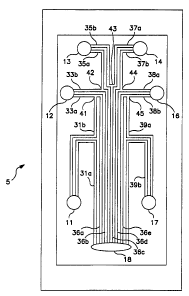
Refernng now to Figure 2, there is shown a working example of a fluidic
microchip in accordance with this invention. The microfabricated device 5
includes a first buffer reservoir 11, a first sample reservoir 12, a second
buffer
reservoir 13, a second sample reservoir 14, a third buffer reservoir 16, a
third
sample reservoir 17, and a waste reservoir 18. A first buffer channel 31a
connects the first buffer reservoir 11 with the waste reservoir 18. A second
buffer
channel 31b connects the first buffer reservoir 11 with a first sample channel
33a
that is in fluid communication with the first sample reservoir 12. The
intersection
of the second buffer channel 31b and first sample channel 33a forms a "tee"
junction 41 with a first waste channel 36a that is in fluid communication with
the
waste reservoir 18. In like manner the second buffer reservoir 13 is connected
to
the first and second sample reservoirs 12 and 14 and to the waste reservoir 18
through channels 33b, 35a, 35b, 36b, 36c, and 37a. Further, the third buffer
reservoir 16 is connected to the second and third sample reservoirs 14 and 17
and
to the waste reservoir i8 through channels 37b, 38a, 38b, 39a, 36d, and 36e.
The
dimensions of the channels 31b, 33a, 33b, 35a, 35b; 37a, 37b, 38a, 38b, and
39a
are selected to provide respective electrical resistances that result in
desired
20 mixing ratios of the various sample and buffer materials at the
corresponding
junctions 41, 42, 43, 44, and 45, for transport to the waste reservoir 18
along the
waste channels 36a, 36b, 36c, 36d, and 36e, respectively.
Microchip 5 is designed and fabricated from a solid substrate material,
preferably, glass. However, such materials as silicon may also be used because
of
the well developed technology permitting its precise and efficient
fabrication.
Although silicon has problems associated with electrical conductivity, such
limitations can be offset by employing insulating layers. Other materials such
as
polymers, quartz, fused silica, sapphire, or plastics are also suitable as
substrate
materials. The surface of the microfabricated device 5 is covered and sealed
by a
_7_
CA 02355084 2001-06-13
WO 00/36390 PCTNS99I29741
cover plate. The substrate includes a microfabricated surface containing
channels
and reservoirs for facilitating the electrokinetic transport of biological and
chemical materials from the reservoirs through the channels of the
microfabricated device 5.
The microchip device 5 is fabricated using micromachining methods
known to those skilled in the art. The micromachining methods available
include
film deposition processes such as spin coating and chemical vapor deposition,
laser fabrication or photolithographic techniques such as visible, ultraviolet
(UV),
or X-ray processes, or etching methods which may be performed by either wet
10 chemical processes or plasma processes. Preferably, the microchannel
configurations of microchip 5 are transferred onto the substrate material
using a
positive photoresist, photomask, and UV exposure. The channels are etched into
the substrate in a dilute, stirred HF/N4HF bath.
The mixing of two or more materials contained in the microfabricated
channels of a microchip device according to this invention is achieved using
electrokinetic transport. A microchip device in accordance with this invention
having a structure like that shown in Figure 2 was fabricated as described
above.
The sample and buffer channels were dimensioned to proportion two streams in
five different channels to demonstrate a multiple dilution experiment.
Channels
20 31a and 39b do not have mixing junctions. The sample and buffer channel
lengths to each tee junction were selected to provide a dilution ratio (sample
/(sample + buffer)) of 0 in Channel 31a, 0.83 in Channel 36a, 0.68 in Channel
36b, 0.52 in Channel 36c, 0.34 in Channel 36d, 0.16 in Channel 36e, and 1 in
Channel 39b. An electrical potential is applied to the sample and buffer
reservoirs 11-16 relative to the waste reservoir 18 to electrokinetically
transport
the materials through the microchip channel manifold. The electrical potential
was applied through platinum wire electrodes which were connected to a single
high voltage source. The required electric field strength to enable
electroosmotic
flow is often between 100V/cm and 1000 V/cm.
_g_
CA 02355084 2001-06-13
WO 00/36390 PCT/US99/29741
To demonstrate the proportioned mixing of the pairs of tributary channels
on the microchip device 5, a dilution experiment of a sample material in a
buffer
material was performed. In Table 1, the lengths of the respective sample and
buffer channels are listed with the calculated dilution ratio (% Sample
Calculated) and the measured dilution ratio (% Sample Measured) for each
channel. The experiment was performed by placing the same sample material in
reservoirs corresponding to first sample reservoir 12, second sample reservoir
14,
and third sample reservoir 17. A diluent was placed in the first buffer
reservoir
11, second buffer reservoir 13, and. third buffer reservoir 16. A 1 kV
potential
10 was applied to the buffer and sample reservoirs and the waste reservoir 18
was
maintained at ground potential.
Microchip performance was monitored by laser induced fluorescence
(LIF) using a charge coupled device (CCD) for imaging and an argon ion laser
beam (514.5 nm, ~ 100 mW) for excitation. The fluorescence signal was
collected
15 using an optical microscope, filtered spectrally (550 nm cut-on), and
measured by
the CCD. The diluent was 10 mM sodium tetraborate, and the sample solution
was rhodamine B (40 p,M) in 10 mM of the buffer solution.
Refernng now to Figure 3, the average fluorescence signal is plotted as a
function of the lateral position across the waste channels. From this plot,
the
20 integrated area allows the determination of the experimental dilution
ratios
which are shown in Table 1. The data presented in Table 1 show good
correlation between the predicted values and the actual values. For channels
36d
and 36e, the actual ratios are higher than expected. As the quality of the
substrate machining improves, it is expected that the ratios will match more
25 closely. Also, the microchips prepared in accordance with this invention
can be
calibrated following fabrication to handle small differences in channel
dimensions which affect the channel resistance.
-9-
CA 02355084 2001-06-13
WO 00/36390 PCT/US99/29741
TABLE 1
Length Length Length % Sample, % Sample,
Channel Sample Buffer Mixing CalculatedMeasured
31 a - 44..8 - 0 0
36a 4.9 24.5 39.7 83 84
36b 5.0 10.4 39.8 68 67
36c 9.6 10.5 39.9 52 51
36d 9.5 4.8 39.8 34 36
36e 24.8 4.7 39.7 16 19
39b 45.1 - - 100 100
*length in mm
Referring now to Figure 2a, an alternative embodiment of a microchip
device in accordance with the present invention is shown having multiple sets
of
mixing junctions configured for minimizing the number of material reservoirs.
The device 90 includes a single sample reservoir 92, a plurality of buffer
reservoirs 94, 96, 98, 100, and 102, and a waste reservoir 110. The sample
material is loaded into the sample reservoir 92. A common buffer, reagent, or
various buffers or reagents are loaded into the buffer reservoirs 94 - 102.
Respective pairs of sample channels 91a, 91b, 93a, 93b, 95a, 95b, 97a, 97b,
and
99a, 99b interconnect the sample reservoir 92 to each of the plurality of
buffer/reagent reservoirs 94-102. Corresponding pairs of mixing channels lOla,
lOlb, 103a, 103b, 105a, 105b, 107a, 107b, and 109a, 109b interconnect each
sample channel with the waste reservoir 110. The mixing channels intersect the
sample channels at mixing junctions l 11a, lllb, 113a, 113b, 115a, 115b, 117a,
117b, and 119a, 119b, respectively. This arrangement allows a large number of
simultaneous, fixed dilutions of the sample material to be performed with one
or
more buffer solutions. The cross-sectional areas and lengths of the channel
segments forming the mixing junctions are dimensioned to provide mixing of the
sample and buffer materials in different, preselected proportions at each of
the
mixing junctions. In this way, the device 90 minimizes the number of
reservoirs
required to do the multiple dilutions of a single sample within a two
dimensional
layout, i.e., without crossing of channels. In general, to perform N
dilutions, N/2
-10-
CA 02355084 2001-06-13
WO 00/36390 PCT/US99/29741
+ 2 reservoirs are required. The value is rounded up to the next higher
integer if
N is an odd number. In a variation of the embodiment shown in Figure 2a, the
plurality of buffer reservoirs are combined into a single reservoir by using
sufficiently small vertical access conduits (vias) through the microchannel
coverplate and a buffer reservoir having a sufficiently large cross section to
access the vias. Alternatively, vias could be used to communicate between
multiple layers of microchannels to allow the reduction of the plurality of
buffer
reservoirs into a single reservoir. The multiple layers of microchannels would
allow channels to cross over the tops of each other similar to the constructs
used
in multilayer printed circuit boards.
Refernng now to Figure 4, there is shown a further embodiment of a
microchip device according to this invention. A microchip 50 includes sample
reservoir 52, buffer reservoir 54, and waste reservoirs 60A-60C. Sample and
buffer reservoirs 52 and 54 supply fluidic materials to an access channel
formed
15 of segments Ll-L4 of microchip device 50. The microchip 50 includes three
mixing channels 58A, 58B, and 58C connected along the access channel and in
fluid communications with the waste reservoirs 60A, 60B and 60C respectively.
Switches 62, 64, or 66 are provided for selectively connecting the waste
reservoirs 60A, 60B, and 60C, respectively to ground potential.
The sample and buffer solutions are mixed in mixing channels 58A, 58B,
and 58C by way of switches 62, 64, or 66 which are provided for connecting a
corresponding one of the waste reservoirs 60A, 60B, or 60C, to ground
potential.
Thus, when channel 58A is connected to ground, channels 58B and 58C would be
disconnected. Thus, for example, in a microchip 50 having access channel
lengths L1 = L2 = L3 = L4, the mixing ratio for channel 58A would be 3 parts
sample (L1) to 1 part buffer (L2+L3+L4). For channel 58B the mixing ratio
would be 1 part sample (Ll+L2) to 1 part buffer (L3+L4), and for channel 58C,
1
part sample (L1+L2+L3) to 3 parts buffer (L4). It is to be understood that the
channel lengths L1, L2, L3, and L4 of microchip SO need not be equal so that
-11-
CA 02355084 2001-06-13
WO 00/36390 PCT/US99l19741
other mixing ratios can be achieved.
Variable Volume Valve
A schematic of a microchip 15 according to the present invention that
demonstrates valuing is depicted in Figure 5. The microchip 15 includes a
sample reservoir 70, a buffer reservair 74, a first waste reservoir 76, and a
second
waste reservoir 78. A sample channel 71 has a first end in fluidic
communication
with the sample reservoir 70. A buffer channel 73 has a first end in fluidic
communication with the buffer reservoir 74. A first waste channel 75 has one
end in fluidic communication with the first waste reservoir 76 and a second
waste
channel 77 has an end in fluidic communication with the second waste reservoir
78. The four channels intersect at a valuing junction 80. The lengths of the
various channels between the respective reservoirs and the valuing junction
are
selected to provide predetermined electrical resistance in the respective
channels.
In this manner, the electric potentials between the various reservoirs and the
valve
junction 80 can be established using a single high voltage source. In a
working
example of microchip 15, the channel lengths listed in Table 2 were used.
The sample reservoir 70 is connected to a high voltage supply 68. A
switch 72 is connected in series between the high voltage supply 68 and the
buffer reservoir 74. The first and second waste reservoirs 76, 78 are
connected at
a ground potential relative to the high voltage supply 68. The valve 80 is
actuated by operating the high voltage switch 72. When switch 72 is closed,
the
valve 80 is closed and the sample material is electrokinetically transported
only to
the first waste reservoir 76. When switch 72 is open, the valve 80 is opened
and
the sample material is transported to both first waste reservoir 76 and second
waste reservoir 78. Because the lengths of first waste channel 75 and second
waste channel 77 are slightly different, the proportion of sample material
transported to the respective waste reservoirs is different. The relative
proportions of sample material are determined according to the relative
electrical
-12-
CA 02355084 2001-06-13
WO 00/36390 PCT/US99/29741
resistances of the first and second waste channels.
To demonstrate the operation of the valve, fluorescent images of an
organic dye used in the working example of the microchip 15 are presented in
Figures 6(a)-6(d). Figure 6a shows a white light image of the valve junction
80
where the buffer, sample, first waste and second waste channels intersect.
Figures 6b-6d show transport of the sample material during a sequence of
having
the valve closed, opened, and reclosed. In Figure 6b, the switch 72 is closed
and
a 1kV potential is applied to the buffer reservoir 74 and sample reservoir 70.
Under those conditions the sample material is transported through the valve
junction 80 and toward the first waste reservoir 76. In Figure 6c, the high
voltage
switch 72 has been opened for 0.4 s and the sample material is transported to
both
the first waste reservoir 76 and the second waste reservoir 78. The volume of
sample material dispensed to the second waste reservoir 78 is proportional to
the
period of time the high voltage switch 72 is open and to the electric field
strength
in the analysis channel 77. Figure 6d shows the sample material plug migrating
down the analysis channel after valve 80 has been reclosed by closing the
switch
72. The electric field strength in each of the channels when switch 72 is
closed
are listed in Table 2. The switch 72 can be embodied as any suitable type of
switch, including mechanically operated switches, a solenoid-operated switch
such as a relay, or a solid state switching device. Alternatively, the
function of
switch 72 can be performed by cycling the voltage level present between the
buffer reservoir 74 and sample reservoir 70 by way of an external control, for
example, such as an independently controlled power supply or switching
circuit.
-13-
CA 02355084 2001-06-13
WO 00/3b390 PCT/US99/29741
TABLE 2
Electric Field
Channel Length (mm) Strength (V/cm) with switch closed
buffer (73) 7.1 400
sample (71 ) 14.8 190
first waste (75) 24.2 300
second waste (77) 25.1 290
A further working embodiment demonstrating valuing in accordance with
the present invention is shown in Figure 7. The device I25 requires fewer
fluidic
reservoirs to effect valuing than the.embodiment shown in Figure 5. Microchip
device 125 reduces the number of waste reservoirs to one because the waste
channel 175 and separation channel 177 transport the combined sample and
buffer materials to a single waste reservoir 178. The buffer channel 173,
sample
channel 171, waste channel 175, and the separation channel 177 are dimensioned
so as to provide appropriate electrical field strengths in the four channels
that
intersect at the valve junction 180. For the proper operation of the gated
valve,
the electrical resistances of the channels are preferably designed so that the
electric field strength in the buffer channel 173 is greater than the electric
field
strength in the separation channel 177 and the electric field strength in the
waste
channel 175 is greater than the electric field strength in the sample channel
171.
Similar to device 15 of Figure 5, a high voltage power supply 168 is directly
connected to the sample reservoir 170 and is connected through the switch 172
to
the buffer reservoir 174. The ground side of power supply 168 is operably
linked
to the waste reservoir 178. The valuing device 125 is actuated in essentially
the
same manner as the device shown in Figure 5. More specifically, when the
electrical switch 172 is opened, the valve 180 is opened, and when the
electrical
switch 172 is closed, the valve 180 closes.
Reagent Mixing Circuit
Referring now to Figure 8, there is shown schematically a standard reagent
- 14-
CA 02355084 2001-06-13
WO 00/36390 PCT/US99/29741
mixing circuit 210 for implementation on a microchip in accordance with the
present invention. The mixing circuit 210 electrokinetically mixes a first
reagent
from R 1 reservoir 211 and a second reagent from R2 reservoir 212 at T3
intersection 213 without any potentials applied to the W1 reservoir 214 and
the
W2 reservoir 215. In this embodiment, the W 1 reservoir 214 and the W2
reservoir 215 are used as current shunts to assist in the delivery of low flow
rates
of the first and second reagents to the T3 intersection 213. The W 1 reservoir
214
and the W2 reservoir 215 each contain some appropriate buffer solution for
executing electrokinetic manipulations. The use of current shunts permits a
wide
range of stable mixing ratios for the reagents with minimal requirements for
voltage control, signal-to-noise ratio, or digital-to-analog quantization
levels.
Without current shunts, low or highly precise voltages applied to the reagent
reservoirs would be required to pump small volumes of material within the
channel manifold. That could lead to unstable delivery of material from the R1
reservoir 211 or the R2 reservoir 212 into the T3 intersection 213, depending
on
the stability of the power supplies when operating at low potentials or
currents.
To deliver a small volume of the first reagent to the T3 intersection 213
using the W 1 reservoir 214 as a current shunt, the material is
electrokinetically
transported from the R1 reservoir 211, and the flow is split at the T1
intersection
216. Controlled portions of the first reagent are sent toward the T3
intersection
213 and the W 1 reservoir 214. The ratio of the split portions is determined
by the
applied potentials and resistances of the channels leading from the R1
reservoir
211 and the W 1 reservoir 214. Likewise, to accurately deliver small volumes
of
the second reagent to the T3 intersection 213 using the W2 reservoir 215 as a
current shunt, the material electrokinetically transported from the R2
reservoir
212 is split at the T2 intersection 217, with a portion of the material
transported
toward the T3 intersection 213 and a second portion transported toward the W2
reservoir 215. This configuration allows delivery of small volumes of material
from either the R1 reservoir 211 or the R2 reservoir 212 to the T3
intersection
-15-
CA 02355084 2001-06-13
WO 00/36390 PCTNS99/29741
213, where they are mixed, and avoids having to use low or highly precise
voltages applied to the material reservoirs themselves. It is understood that
all
the electric potentials referred to in connection with the description of this
embodiment are relative to the waste reservoir 219.
An alternate operation of the mixing circuit shown in Figure 8 is to use the
W 1 reservoir 214 and the W2 reservoir 215 to dilute the reagent materials
from
the R1 reservoir 211 and the R2 reservoirs 212, respectively, prior to their
being
mixed at the T3 intersection 213. To dilute the material in the R1 reservoir
211
with material from the W1 reservoir.214, electric potentials are applied to
both
the R1 reservoir 211 and the W1 reservoir 214 to transport the materials from
the
respective reservoirs towards the Tl intersection 216. The amount of dilution
of
the first reagent by the buffer material in the W 1 reservoir 214 at the T1
intersection 216 depends on the magnitudes of the potentials applied to the
reservoirs and the resistances in the respective channels. Similarly, to
dilute the
material from the R2 reservoir 212 with the buffer material from the W2
reservoir
215, electric potentials are applied to both the R2 reservoir 212 and the W2
reservoir 215 to transport the materials from the respective reservoirs toward
the
T2 intersection 217. The amount of dilution of the second reagent by the
buffer
material in the W2 reservoir 215 at the T2 intersection 217 depends on the
magnitudes of the potentials applied to the respective reservoirs and the
resistances in the channels. By using the first and second buffers to dilute
the
first and second reagents, respectively, a wider concentration range of
reagents
can be reacted at the T3 intersection and studied in the reaction channel 218.
In either of these embodiments, W 1 reservoir 214 and the W2 reservoir
215 may be left electrically floating (i.e., with no connection to an external
circuit) and the fluidic circuit will function principally like a tee junction
similar
to that shown in Figure 1. That is, the first reagent and the second reagent
will be
mixed in proportions dictated by the applied potentials, the geometry of the
channels, and the chemical characteristics of the materials in those channels.
It
-16-
CA 02355084 2001-06-13
WO 00/36390 PCTNS99/29741
will be appreciated that either of the buffer reservoirs 214 or 215 can be
left
electrically floating while the other is controlled with a suitable power
supply.
Referring now to Figure 9, there is shown an alternate embodiment of the
dilution/mixing circuit shown in Figure 8. In the circuit shown in Figure 9,
multiple fluid shunts are included to provide increased dynamic range over the
dilution of either the first reagent in Rl reservoir 221, the second reagent
in R2
reservoir 222, or both. The flow of the first reagent through T1 intersection
223
operates just as the corresponding intersection of the embodiment shown in
Figure 8 and described above. The flow of the first reagent from the TI
intersection toward T7 intersection 230 can be further diluted at T3
intersection
224 with a first diluent held in D1 reservoir 225. W3 reservoir 227 allows a
material shunting process to occur similar to that which occurs at the T1
intersection 223. This serial dilution process can continue with additional
fluidic
elements that comprise an input channel, an output channel, a diluent channel,
and a shunting channel all connected at a four-way intersection. The
reservoirs
and intersections on the right hand side of T7 intersection 230 mirror the
reservoirs and intersections shown on the left hand side of that intersection.
They perform similar operations, but carry out the dilution process on the
second
reagent which is held in R2 reservoir 222. The circuit depicted schematically
in
Figure 9 allows independent control over all of the reagent, diluent, and
waste
(shunting) reservoirs for maximal control of the process. In general, the
diluents
would be the same, but they could also be different. An operationally less
complex circuit that can perform a similar dilution function can be produced
by
making the left-hand-side and right-hand-side diluent and waste reservoirs,
respectively common. Such a device is shown in Figure 10 below.
Serial Dilution Circuit
The microfluidic circuit of the present invention can be further embodied
as a serial diluter. In a serial diluter according to this invention, a series
of
-17-
CA 02355084 2001-06-13
WO 00/36390 PCTNS99/29741
channels, tees, and intersections are configured for mixing two reagents (a
sample
and a buffer) in a series of preselected ratios. The desired dilutions
correspond to
the current flow in the various channels of the microchip. Therefore, a
microchip
for implementing this aspect of the present invention is designed by analyzing
the
various channels as an equivalent electrical circuit. Each channel or circuit
branch has a resistance designed to provide a desired electrical current
therethrough. The sample and buffer materials are transported through the
various microchannels in direct proportion to the equivalent current flow.
Figure
shows a preferred microfluidic circuit 810 for a serial diluter in accordance
10 with this aspect of the present invention.
Refernng now to Figure 10, the serial diluter circuit 810 includes a buffer
reservoir 812 for holding a buffering material or other diluent, a sample
reservoir
814 for holding a sample material, a first waste reservoir 816, and a second
waste
reservoir 818. A main buffer channel 821 in fluid communication with the
buffer
reservoir 812 is formed for carrying the buffer material. A sample channel 822
is
in fluid communication with the sample reservoir 814 for carrying the sample
material.
A plurality of buffer channel extensions 821a, 822a, 823a, and 824a
extend in series from the buffer channel 821. A set of buffer branch channels
821b, 822b, 823b, 824b, and 825b each branch off from the buffer channel
extensions 821a, 822a, 823a, and 824a, respectively, at selected locations
relative
to the intersection with the main buffer channel 821. The sample channel 822
interconnects with the buffer branch channel 821b at a preselected distance
from
the intersection with the first buffer extension channel 821a. A mixing
channel
821c interconnects with the buffer branch channel 821b at the point of
intersection with sample channel 822. A series of mixing channels 822c, 823c,
and 824c extend from the other end of mixing channel 821c. A set of analysis
channels 821 d, 822d, 823d, 824d, and 825d branch off from the mixing channels
821c, 822c, 823c, and 824c, respectively, at selected locations relative to
the
-18-
CA 02355084 2001-06-13
WO 00/36390 PCTNS99/29741
intersection with the branch channel 821b. In the embodiment shown in Figure
10, the analysis channels branch off at respective ends of the mixing
channels.
The analysis channels have different lengths relative to one another and are
in
fluid communication with the second waste reservoir 818. A waste channel 826
interconnects the end of mixing channel 824c with the first waste channel 816.
When a single voltage is applied to the buffer reservoir 812 and the
sample reservoir 814 relative to the waste reservoirs 816 and 818, the buffer
material is electrokinetically transported along buffer channel 821 into
buffer
channel extension 821a and buffer branch channel 821b. The buffer material is
similarly transported from buffer branch channel 821b into mixing channel
821c.
Arrows indicate the buffer flow direction in the drawing. Simultaneously, the
sample material is electrokinetically transported along sample channel 822
into
mixing channel 821c and analysis channel 821d as indicated by the arrows in
Figure 10. The sample material is diluted with the buffer material in mixing
channel 821c, whereas the sample material in analysis channel 821d is at the
same concentration as the sample material in sample channel 822, i.e., it is
undiluted.
As the process continues, the buffer material in buffer extension channel
821a is split between buffer extension channel 822a and buffer branch channel
822b. The buffer material in branch channel 822b flows into mixing channel
822c and the diluted sample material in mixing channel 821c is split between
mixing channel 822c and analysis channel 822d. The diluted sample material
from mixing channel 821c is further diluted in mixing channel 822c, whereas
the
diluted sample material in analysis channel 822d is at the same concentration
as
the diluted sample material in mixing channel 821c.
It can be readily appreciated that further splitting and dilution of the
sample and buffer materials is accomplished in a similar fashion with buffer
extension channels 823a and 824a, buffer branch channels 823b, 824b, and 825b,
mixing channels 823c and 824c, and analysis channels 823d, 824d, and 825d. In
- 19-
CA 02355084 2001-06-13
WO 00/36390 PCTNS99I29741
the embodiment shown in Figure 10, there are five analysis channels, but the
series of channel extensions, channel branches, mixing channels, and analysis
channels can continue for as many dilutions as needed for a particular
process.
In the embodiment of Figure 10, the channels are formed with essentially
the same cross-sectional areas. The channel resistance is increased by
lengthening the channel or decreased by shortening the channel during design
and
fabrication of the microchip. Use of relatively narrow cross sections for the
mixing channels is preferred because it allows rapid equilibration of the
mixed
fluid streams.
As an example of the serial diluter described above and shown in Figure
10, a microchip device having the channel structure shown in Figure 10 was
fabricated. A CCD image of the actual embodiment of the serial diluter circuit
810 is shown in Figure 11(a). The various sample and buffer channels were
dimensioned to proportionally dilute the sample material at various
concentrations. The channel dimensions were selected to provide the following
sample dilutions: channel 821d, 100% sample; channel 822d, 38% sample and
62% buffer; channel 823d, 22% sample and 78% buffer; channel 824d, 14%
sample and 86% buffer; and channel 825d, 6% sample and 94% buffer. The
lengths of the various channels on the microchip are presented in Table 3
below
in millimeters (mm).
-20-
CA 02355084 2001-06-13
WO 00/36390 PCT/US99/29741
TABLE 3
Channel ID Length
Buffer Channel 821 5.7mm
Sample Channel 822 15.6mm
Buffer Extension Channels 0.2mm each
821a,
822a, 823a, and 824a
Buffer Branch Channels 821b,O.lmm each
822b,
823b, 824b, and 825b
Mixing Channels 82.1c, 822c,0.4mm each
823c,
and 824c
Waste Channel 826 S.Omm
Analysis Channel 821d l2.Omm
Analysis Channel 822d 11.9mm
Analysis Channel 823d 11.8mm
Analysis Channel 824d 11.9mm
Analysis Channel 825d l2.Omm
An experiment was run using the microchip for serially diluting a sample
material (100~,M rhodamine B in 20rnM sodium tetraborate) with a buffer
material (20mM sodium tetraborate). The sample and buffer reservoirs were
filled with the respective sample and buffer materials. A 400 volt potential
was
applied to the sample and buffer reservoirs while the waste reservoirs were
maintained at ground potential. Figure 11(b) is a fluorescence image showing
the
progressive dilution of the sample, which is readily observable in the
successive
analysis channels. The average fluorescence intensity of the respective
analysis
channels is plotted in Figure 12 as a function of pixel position. The
calculated
and measured dilution ratios for the diluted material in each analysis channel
are
set forth in Table 4.
-21-
CA 02355084 2001-06-13
WO OOI36390 PCTNS99/29741
TABLE 4
Channel Relative DilutionRelative Dilution
(Calculated) (Measured)
821 d 1.0 1.0
822d 0.37 0.36
823d 0.22 0.21
824d 0.12 0.13
825d 0.052 0.059
The data presented in Table 4 show that there is good correlation between
the theoretical and actual dilution ratios. The calculated relative dilutions
are
corrected for slight variations in channel widths. Also, the measured relative
dilutions are corrected for nonuniform excitation for the fluorescence
measurements.
In view of the foregoing disclosure, it can be seen that the microfabricated
device in accordance with the present invention readily provides microfluidic
proportioning. Such functionality is useful in analyzing chemical and
biological
reactions such as kinetics studies requiring the combination of materials in
precise volumes. The microfabricated device disclosed herein enables the on-
chip mixing of materials in different proportions using channels having
different
electrical resistances. The microfabricated device includes one or more
channel
junctions or "tees" having sample and buffer reagent channels that meet at a
mixing junction. By having tributary channels with the same cross sectional
area
but different lengths, the materials traveling therethrough, can be mixed at a
junction depending on the ratio of the channel lengths, because the electrical
resistances of the microfabricated channels are directly proportional to the
channel length. Microfabricated channels having different cross-sectional
areas
could also effectively proportion samples, because the microchannel resistance
is
inversely proportional to cross-sectional area. As such, handling of the
voltage
division on the microchip can be accomplished by properly dimensioning the
-22-
CA 02355084 2001-06-13
WO 00/36390 PCT/US99/29741
channels of the microfabricated device without using techniques external to
the
microchip. In this way, the number of voltage sources needed to operate a
nucrofluidic device can be greatly reduced. Furthermore, by appropriate
arrangement and dimensioning of the microchannels and their interconnections,
the number of sample, buffer, and waste reservoirs needed to perform multiple
dilutions of a sample material can be significantly reduced.
The terms and expressions which have been employed are used as terms of
description and not of limitation. There is no intention in the use of such
terms
and expressions of excluding any equivalents of the features shown and
described
or portions thereof. For example channel resistance can be varied by altering
channel width or height as well as length to facilitate compact microfluidic
designs. It is recognized, however, that various modifications such as channel
dimension, location, and arrangement are possible within the scope of the
invention as claimed.
-23-