Note: Descriptions are shown in the official language in which they were submitted.
CA 02355156 2001-06-13
WO 00/36580 PCT/US99/17990
REVERSIBLE ELECTROCHEMICAL MIRROR FOR MODULATION OF
REFLECTED RADIATION
BACKGROUND OF THE INVENTION
This invention is concerned with devices, such as mirrors and windows, having
controllable transmittance and reflectivity.
Sunlight transmitted through windows in buildings and transportation vehicles
S can generate heat (via the greenhouse effect) that creates an uncomfortable
environment
and increases air conditioning requirements and costs. Current approaches to
providing
"smart windows" with adjustable transmission for use in various sunlight
conditions
involve the use of light absorbing materials. These approaches are only
partially effective,
since the window itself is heated and because these devices, such as
electrochromic
devices, are relatively expensive and exhibit limited durability and cycle
life. Certain
liquid crystal-based window systems switch between transmissive and
opaque/scattering
states, but these systems require substantial voltages to maintain the
transparent state.
There is an important need for an inexpensive, durable low voltage smart
window with
variable reflectivity. Reflecting the light, rather than absorbing it, is the
most efficient
1 S means for avoiding inside heating.
In prior art attempts to exploit reversible electrodeposition of a metal for
light
modulation, the deposits obtained on transparent substrates presented a rough
and black,
gray, or sometimes colored appearance (typical of finely-divided metals) and
exhibited
poor reflectivity and high light absorbance, especially when thick. This was
true in the
work of Udaka, for example, even when the transparent conductor electrode
surface had
been metallized (Udaka, et al., published European Patent Application No.
0712025,
Application No. 9S 117797.1 ). Such deposits have been investigated for
display
applications involving reflectance from the background, with white pigments
often being
added to improve contrast. Warszawski (U.S. Patent No. 5,056,899), which is
concerned
2S with displays, teaches that reversible metal electrodeposition is most
appropriate for
display applications, since significant disadvantages for transmission devices
were given
(e.g., the possibility of metal deposition at the counter electrode). Such
teachings imply
that the application of reversible metal deposition to smart windows must
involve light
CA 02355156 2001-06-13
WO 00/36580 PCTNS99/17990
2
absorption by the finely divided electrodeposited metal, which would result in
heating of
the device itself and thus the space inside. The prior art literature also
teaches that, for
transmission-type devices, reversible metal electrodeposition requires the use
of an
auxiliary counter electrode reaction; otherwise, metal would plate on the
counter
S electrode as the deposit was de-plated from the working electrode.
Electrolytes described in the prior art literature contain auxiliary redox
species
(e.g., bromide, iodide, or chloride) that are oxidized (e.g.. to bromine,
iodine, or chlorine)
at the counter electrode during metal deposition, introducing chemistry-
related
instabilities during long term operation and greatly reducing the memory
effect by
causing dissolution of the metal deposit on open circuit, e.g., 2Ag + Br2 --->
2AgBr.
In most cases, this auxiliary redox process hinders metal deposition at the
counter
electrode during erasure of the light modulating deposit, introducing a
threshold voltage
that is desirable for display applications. This auxiliary redox process
represents a
significant side reaction even when metal plating/deplating occurs at the
counter
1 S electrode and a threshold voltage is not observed. See, e.g., Warszawski,
Columns 3-4
(when copper or nickel were present in the counter electrode paste) and
Duchene, et al.,
Electrolytic Display, IEEE Transactions on Electron Devices, Volume ED-26,
Number
8, Pages 1243-1245 (August 1979); French Patent No. 2,504,290 (October 22,
1982).
I-Iigh switching voltages of at least 1 V were used for all the
electrodeposition devices
which have been found in the patent and literature prior art.
Warszawski teaches that the.use of a grid counter electrode would give a less
uniform deposit since deposition on the transparent working electrode is
highly localized
in the vicinity of the counter electrode grid lines (a consequence of the very
thin film of
gel electrolyte used). Warszawski also teaches the use of an aqueous gel
electrolyte to
2S minimize sensitivity to atmospheric contaminants and to avoid the necessity
of having
a leak tight seal. Such electrolytes, however, have much more limited
temperature and
voltage operating ranges compared with organic-based electrolytes with high
boiling
solvents.
Prior art literature teaches that the memory effect is temporary. This is a
consequence of the occurrence of a counter electrode reaction other than metal
plating/deplating. The energetic oxidation products generated at the counter
electrode can
CA 02355156 2001-06-13
WO 00/36580 PCT/TJS99/17990
3
cause dissolution of the metal deposit on the working electrode either
chemically on open
circuit (slow) or electrochemically during short circuit (fast).
None of the reversible electrodeposition devices known in the prior art have
exhibited high-reflectivity mirror deposits as needed for applications
requiring adjustable
reflectivity. Reversible electrodeposition of mirror deposits, for example,
could be used
to automatically adjust the reflectivity of automotive rear and side view
mirrors for
optimum viewing under various lighting conditions. In particular, dissolution
of some or
all of the mirror deposit from a transparent electrode on a glass or plastic
substrate could
reduce mirror glare from headlights of following vehicles. The reversible
electrodeposition approach for adjustable mirrors offers significant cost and
safety
advantages compared to available electrochromic mirrors, which require a
relatively
invariant cell gap and involve toxic chemicals (e.g., viologen).
SUl~iII~AItY OlF THE INVENTION
The electrochemical mirror of this invention permits efficient and precise
control
over the reflection of visible light and other electromagnetic radiation. The
mirror
includes a transparent first electrode, a surface modification layer on the
first electrode,
and a second electrode. An electrolytic solution is disposed between the first
and second
electrodes such that ions of a metal which can electrodeposit on the first and
second
electrodes are soluble in the electrolytic solution.
When a negative electrical potential is applied to the first electrode
relative to the
second electrode, the applied potential tends to cause deposited metal to be
dissolved
from the second electrode into the electrolytic solution and to be
electrodeposited from
the solution onto the first electrode. The surface modification layer
facilitates
substantially uniform nucleation of the electrodeposited metal in a mirror
surface on the
first electrode, such that the amount of deposited metal subsisting on the
first electrode
affects the reflectivity of the mirror for the radiation. Conversely, when the
polarity is
reversed and a positive electrical potential is applied to the first electrode
relative to the
second electrode. the applied potential tends to cause deposited metal to be
dissolved
from the first electrode and electrodeposited from the solution onto the
second electrode,
thereby decreasing the reflectivity of the mirror. The reflectivity of the
mirror deposit can
CA 02355156 2001-06-13
WO 00/36580 PCT/US99/17990
4
be selectively adjusted from near 0% to almost 100%, depending on the amount
of metal
deposited on the conducting film.
In various embodiments, the second electrode may be a continuous or
discontinuous electrical conductor. An underlayer may be provided between the
second
S electrode and the second substrate to improve adhesion.
The first electrode may be disposed uniformly on a first substrate, or may be
disposed in a pattern. The surface modification layer may be a thin layer
(i.e., sufficiently
thin to be nominally transparent) of an inert metal which is electrochemically
more stable
towards oxidation than the electrodeposited metal. The surface modification
layer may
also be disposed uniformly on the first electrode, or may be disposed in a
pattern. An
underlayer may be added between the first electrode and the surface
modification layer
to improve adhesion.
The electrolytic solution may include a gelling agent to form an aqueous or a
non-
aqueous gel electrolyte.
DESCRIPTION OF THE DRAWINGS
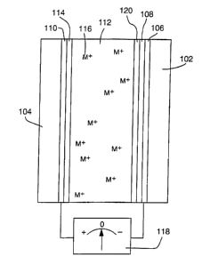
Figure 1 is a cross sectional view depicting the general design of an
electrochemical minor constructed according to the invention for modulation of
reflected
radiation.
Figure 2 is a cross sectional view similar to Figure 1, but illustrating the
state of
the mirror when sufficient negative electrical potential has been applied to
the first
electrode relative to the second electrode to cause substantial quantities of
the metal to
deposit onto the first electrode.
Figure 3 is a cross sectional view similar to Figures 1 and 2, but depicting
the
state of the mirror when sufficient positive electrical potential has been
applied to the first
electrode relative to the second electrode to cause substantially all of the
metal to deposit
on the second electrode.
CA 02355156 2001-06-13
WO 00/36580 PCTNS99/17990
DESCRIPTION OF THE INVENTION
Figure 1 is a cross sectional view depicting the general design of an
electrochemical mirror constructed according to our invention (some
dimensions,
particularly layer thicknesses, are disproportionate in the drawings in order
to more
5 effectively illustrate the structure and function of the invention). The
mirror, which
allows precise, reversible control over the reflection of electromagnetic
radiation,
includes a first substrate 102, which is substantially transparent to the
radiation to be
controlled, and a second substrate 104. An electrically conducting film 106,
which is also
substantially transparent, is deposited on the first substrate. The film 106,
with the
addition of an electrochemically stable surface modification layer 108,
functions as a
first electrode. A second electrode 110 is deposited on the second substrate
104. The
second electrode can alternatively be a bulk electrode, a metal plate or sheet
for example,
with sufficient rigidity that the second substrate 104 would not be needed.
The second
electrode 110 is electrochemically stable or is covered with a sufficient
thickness of an
active metal layer 114 to avoid exposure of the second electrode surface. The
surface of
electrode 110 may be roughened to reduce reflection of radiation from the
electrode or
to improve switching speed by lowering the current density.
An electrolytic solution 112 is located between and in electrical contact with
the
electrodes 106 and 110. In the configuration depicted by Figure 1, the mirror
may be
initially charged by depositing the metallic layer 114 on the electrode 110,
i.e., the layer
114 is deposited on the electrode 110 prior to assembly of the mirror. As
those skilled in
the art will appreciate, and as further explained in the discussion below
regarding the
operation of the mirror, such a metallic layer may, alternatively, be
initially deposited on
the electrode 110, on the electrode 106 (i.e., on the surface modification
layer 108 as a
layer 120), or, as depicted in Figure 1, divided between a partial deposit on
the electrode
106 and a partial deposit on the electrode 110. If the electrode 110 is not
itself composed
of the mirror metal, the amount of metal in these initially deposited layers
constitutes the
maximum amount of metal which will be available for deposit, as explained in
more
detail below, to control the reflectivity of the mirror. Metal ions 116, which
contain the
same metal atoms as the layers 114 and 120, are dissolved within the
electrolytic solution
112 such that the metal atoms in solution can be reversibly electrodeposited
on and
CA 02355156 2001-06-13
WO 00/36580 PCT/US99/17990
6
electrodissolved from the first and second electrodes. The surface
modification layer 108
applied to the first electrode 106 facilitates the nucleation on this
electrode of
electrodeposited metal from the ions 116.
The mirror is intended for use in conjunction with a source of electrical
potential
S 118, which has a reversible polarity and adjustable or pre-set positive and
negative
potential values, connected between the first and second electrodes 106 and
110. When
a negative electrical potential is applied to the first electrode 106 relative
to the second
electrode 110, metal 114 deposited on the second electrode 110 will tend to be
dissolved
from the second electrode into the electrolytic solution 112, while metal ions
116 in the
solution will tend to be electrodeposited from the solution onto the surface
modification
layer 108 of the first electrode 106. The surface modification layer 108 will
tend to cause
the metal to deposit in a substantially uniform layer, forming a mirror
surface.
When the polarity of the applied potential is reversed, such that a positive
potential is applied to the first electrode 106 relative to the second
electrode 110,
deposited metal will tend to be dissolved from the first electrode into the
solution 112 and
dissolved metal will tend to be electrodeposited from the solution onto the
second
electrode.
The amount of deposited metal which remains on the first electrode will
determine the reflectivity which the mirror demonstrates for radiation. The
process is
reversible and may be maintained at virtually any point between substantially
complete
deposition on and substantially complete erasure from the first electrode 106.
Thus the
mirror may be adjusted to any reflective value from approximately 0%
reflective to
approximately 100% reflective. The lower limit of reflectivity for the mirror
is affected
by the reflectivities of the nucleation layer 108, the electrode 106, and the
substrate 102;
these reflectivities may be reduced by use of anti-reflection coatings of the
type
commonly employed, or by adjusting the layer thicknesses.
Figure 2 is a cross sectional view similar to Figure 1, but illustrating the
performance of the mirror when sufficient negative electrical potential has
been applied
to the first electrode relative to the second electrode for a sufficient
period of time to
cause a substantial layer of the metal to deposit onto the first electrode. In
this condition,
the layer 120, created by the deposited metal, will function as a highly
reflective mirror
CA 02355156 2001-06-13
WO 00/36580 PCTNS99/17990
7
and will tend to reflect radiation, illustrated by the light beam 122, which
impinges on
the mirror.
Figure 3 is a cross sectional view similar to Figures 1 and 2, but
illustrating the
behavior of the mirror when sufficient positive electrical potential has been
applied to the
S first electrode relative to the second electrode for a sufficient period of
time to cause
substantially all of the metal to dissolve from the first electrode and to
deposit as the
metallic layer 114 on the second electrode. In this condition, the mirror will
impose a
minimal impediment to incoming radiation, thereby allowing substantially all
such
incoming radiation to be transmitted through the first electrode 106 and
surface
modification layer 108 and to then be absorbed or dispersed by the electrolyte
112 or the
deposited metal 114 on the second electrode 110, as illustrated by the light
beam 124.
Alternatively, the transmitted light might be absorbed or dispersed by a gel
matrix if a
gelled electrolyte is employed. An absorbing dye might also be added to the
electrolyte
or gel matrix to enhance light absorption. For the configuration depicted in
Figure 3, the
amount of reflected light will be minimal.
CA 02355156 2001-06-13
WO 00/36580 PCTNS99/17990
8
)Fabrication of a Preferred Embodiment
The preferred first electrode utilizes a glass or plastic substrate which is
uniformly
coated on one side with an optically transparent, low resistivity (about 10
SZ/square) ITO
(indium tin oxide] or FTO (fluorine-doped tin oxide) film. An adherent inert
metal, such
as Pt, is vapor deposited, preferably by sputtering, onto the ITO or FTO
surface to
enhance the rate of nucleation for metal deposition to yield a mirror deposit;
other
electrochemically inert metals can also be used, e.g., gold, palladium,
rhodium, iridium,
ruthenium, rhenium, etc. It may be advantageous in some cases to employ a
duplex metal
film, e.g., Ti/Au or Cr/Au, in which the underlayer metal (e.g., Ti or Cr)
serves to
improve adhesion of the noble metal to the substrate. An electrical bus
connection is
formed around the perimeter of the ITO or FTO coating.
For an adjustable reflectivity mirror, the preferred second electrode includes
a
sheet of the mirror metal (silver, for example) or of another metal, which has
been
roughened (by bead blasting, for example) to reduce reflection of radiation
from the
second electrode. When the second electrode is not electrochemically stable
under the
operating conditions, an excess amount of mirror metal is used so that the
second
electrode is always covered with the mirror metal and is not exposed to the
solution.
Alternatively, a protective layer of an electrochemically inert metal. such as
platinum, is
used between the reactive substrate and the mirror metal. Prior to cell
assembly, the
second electrode. if other than the minor metal, is plated with a quantity of
mirror metal
sufficient to provide the desired amount of reflectivity when deposited on the
first
electrode and to prevent exposure of the second electrode substrate metal to
the
electrolyte. (Alternatively, the first electrode can be plated with the mirror
metal).
The preferred electrolyte is a gel electrolyte that is both chemically and
electrochemically stable except with regard to electrodeposition of the mirror
metal.
Preferably, the mirror metal is silver added to the electrolyte as a silver
halide and
stabilized in the electrolyte by addition of an excess of halide ions derived
from addition
of a halide salt having a cation that is not electroactive (e.g., lithium,
sodium or
potassium). Other mirror metals having relatively low toxicity and good
electrochemical
characteristics include copper and bismuth. A mixture of halide ions
(chloride, iodide,
bromide) may be employed. The solvent is chosen with respect to its freezing
and boiling
CA 02355156 2001-06-13
WO 00/36580 PCTNS99/17990
9
point to provide the desired temperature operating range, as well as good
electrolyte
stability and good mirror cycling characteristics. Preferred solvents include
water,
dimethylsulfoxide (DMSO), ethylene glycol, gamma-butyrolactone (GBL), dimethyl
formamide (DMF) and mixtures of these. In some cases, it may be necessary to
add other
species to improve the deposit properties, facilitate electron transfer, or
stabilize the
mirror metal in the electrolyte. For example, Ag(I) and Cu(I) can also be
stabilized by
nitriles, amines, phosphines, sulfur donors, etc., e.g. [Cu(nitrile)4]CF3 S03.
Additives that
are electroactive or decomposed during electrodeposition of the mirror metal,
such as
organic compounds normally used for leveling and brightening electrodeposits,
should
be avoided since they would limit the mirror cycle life.
Although the mirror of this invention can be fabricated using a liquid
electrolyte,
use of an electrolyte stiffener is preferred to facilitate mirror fabrication,
to minimize
electrolyte loss that may affect mirror performance or create a chemical
safety hazard,
and to adhesively hold glass fragments formed during accidental breakage that
could
I S otherwise cause physical personal injury. Preferred electrolyte stiffeners
include organic
gelling agents, e.g., polyacrylonitrile (PAN), polyvinylalcohol (PVA),
polyvinylacetate
(PVOAc), and polymethylmethacrylate (PMMA), which dissolve in liquid
electrolytes
to form transparent plastic-like gels at ambient temperatures. With an
appropriate amount
of gelling agent, the electrolyte can retain the conductivity of the liquid
electrolyte, yet
be cut and applied as a "solid state" component. The specific organic polymer
gelling
agent is chosen based on chemical and electrochemical compatibility with a
given
electrolyte and metal mirror reaction. Other possible electrolyte stiffeners
include porous
solid polymers that absorb large quantities of electrolyte, e.g., ormasils and
porous
polypropylene.
The reversible electrochemical cells of this invention can be fabricated using
spacers and a polymer sealant, or using a gasket or o-ring to provide both the
proper
spacing and a seal. The spacer and seal materials must be chemically
compatible with the
electrolyte. Good results have been obtained with polypropylene spacers and
silicone
sealants. The preferred electrode separation is about 0.05 - 3.0 mm.
Electrical contact is
made to the metal bus on each electrode and connected to a voltage source for
switching.
Examples
CA 02355156 2001-06-13
WO 00/36580 PCT/US99/17990
1. An adjustable reflectivity cell having a viewing area of 7.6 x 12.7 cm was
constructed
using a mirror electrode comprised of a 30 ~ sputtered platinum nucleation
layer on
11 ohm/square FTO film on a glass substrate. The counter electrode was a 25 um
thick silver foil (99.99% purity) that had been roughened by bead blasting (
170 grit]
5 and was mechanically supported by a thick plastic backing plate. The
electrolyte was
U.15 M AgI + 1.8 M LiCI in a DMSO solvent. A silicone gasket provided a seal
and
an electrode spacing of 2.4 mm. This cell exhibited excellent mirror formation
and
erasure during deep cycling between -0.5 V (relative to the mirror electrode)
for 25
s and +0.25 V for 65 s for 46,000 cycles. Although mirror formation remained
10 practically uniform, redistribution of the counter electrode silver
resulting in exposure
of the backing plate was eventually observed. Separate experiments showed that
exclusion of oxygen from the electrolyte is necessary to avoid chemical
dissolution
of silver metal that can cause mirror loss on open circuit and possibly
contribute to
silver metal redistribution.
2. An adjustable reflectivity cell having a viewing area of 7.6 x 12.7 cm was
constructed
using a mirror electrode comprised of a 30 ~ sputtered platinum nucleation
layer on
11 ohm/square FTO film on a glass substrate. The counter electrode was 25 um
thick
silver electrodeposited from a commercial plating bath on a copper plate that
had
been roughened by sanding (400 grit). Cell fabrication procedures and the
electrolyte
were the same as for Example 1. This cell also exhibited excellent mirror
formation
and erasure and was cycled between -0.4 V for 25 s and +0.25 V for 65 s for
100,000
cycles without significant degradation in the mirror quality.
Features of the Invention
To attain the uniform metal deposition needed for mirror-like reflectivity, it
is
generally necessary to treat the transparent conducting film of the first
electrode to
improve nucleation, e.g., by vapor deposition of a very thin, yet optically
transparent
(~15-200 ~) "seed" layer of an electrochemically inert metal (e.g., platinum
or gold).
This seed layer minimizes metal deposition overvoltage and enhances the rate
of
nucleation so that mirror deposits are obtained. Other surface treatments
(e.g..
electrodeposition of an inert metal layer) could be used to improve metal
nucleation and
provide mirror deposits. In order to be effective for producing mirror
deposits, the
CA 02355156 2001-06-13
WO 00/36580 PCTNS99/17990
11
nucleation layex must be microscopically continuous, which may not be the case
for some
metallization treatments on some transparent conductor substrates. For
example, the two-
step process commonly used to metallize printed wiring boards prior to copper
plating
(involving palladium displacement of adsorbed tin ions) may not produce
sufficiently
continuous films with adequate adhesion. For special effects, e.g., a
decorative mirror
design. the transparent conductor (e.g., ITO or FTOI and/or the metal
nucleation layer can
be patterned as desired.
Also useful in attaining a mirror deposit are additives that adsorb on the
electrode
surface_ thereby inhibiting the metal deposition process, and additives that
complex the
mirror metal ions, thereby raising the overvoltage for metal deposition. Most
of the
organic addition agents used in the plating industry to brighten and level
deposits,
however, are electrochemically consumed during the metal deposition process
and would
be inappropriate.
No chemically reactive species are produced, since the same metal
1 S deposition/dissolution reaction occurs at both electrodes. As a result, a
particular
switched state is maintained indefinitely at open circuit if oxidizing
contaminants are
excluded from the cell.
The mirror of this invention is an electroreflective device (light reflection
changed
by application of voltage), rather than an electrochromic device (light
absorption changed
by applied voltage) as is typical of the devices taught in the prior art.
The electrochemical mirror is operated well within the electrolyte stability
region,
so that excessive metal plating or deplating is not harmful. In fact, the
mirror is self
limiting for the mirror electrode when biased within the voltage stability
region, since the
current will practically cease when the deposited metal is depleted at that
electrode. By
limiting the amount of mirror metal deposited on the second electrode prior to
cell
assembly, overplating of the first electrode under a protracted applied
voltage can also
be precluded.
No cell separator is required, since the same redox couple (metal
deposition/dissolution) involving a solid product is used at both electrodes,
so that side
reactions are avoided. On the other hand, a porous cell separator, e.g.,
porous
polypropylene, may be used to provide a matrix for containing a liquid
electrolyte and to
CA 02355156 2001-06-13
WO 00/36580 PCTNS99/17990
12
prevent shorting of the two electrodes in the event of extreme flexure of the
cell.
A, wide temperature operating range is obtained by using electrolytes based on
high boiling organic solvents, e.g., dimethylsulfoxide, ethylene glycol,
propylene
carbonate, sulfolane, y-buryrolactone, tetraglyme, etc. Use of mixtures of
these solvents
can extend the temperature range to lower operating temperatures.
Use of a "solid state" gel electrolyte which incorporates an electrochemically
inert
polymer stiffener facilitates mirror fabrication, minimizes the possibility of
chemical or
physical personal injury, and reduces sensitivity to cell leakage and
atmospheric
contamination by preventing convectional transport (diffusion is a very slow
process).
~Che preferred embodiments of this invention have been illustrated and
described
above. lVlodifications and additional embodiments, however, will undoubtedly
be
apparent to those skilled in the art. Furthermore, equivalent elements may be
substituted
for those illustrated and described herein, parts or connections might be
reversed or
otherwise interchanged, and certain features of the invention may be utilized
independently of other features. Consequently, the exemplary embodiments
should be
considered illustrative, rather than inclusive, while the appended claims are
more
indicative of the full scope of the invention.