Note: Descriptions are shown in the official language in which they were submitted.
CA 02355307 2003-10-16
76307-54
1
FABRICATING A HYBRID IMAGING DEVICE
Statement as to Federally Sponsored Research
The invention described herein was made in the
performance of work under a NASA contract, and is subject to
the provisions of Public Law 96-517 (35 USC 202) in which
the Contractor has elected to retain title.
Technoloaical Field
This application relates to fabricating a device
for use in detecting or imaging electromagnetic radiation,
such as photons of light.
Background
Many scientific endeavors, especially space
exploration and astronomical measurement applications,
require highly sensitive electromagnetic radiation.
CA 02355307 2001-06-18
WO 00/38217 PCT/US99/29653
2
detectors, such as photon detectors. Charge-coupled
detectors (CCDs) provide high quantum efficiency, broad
spectral response, low readout noise, and high
resolution. Therefore, CCD devices have been used
extensively in scientific applications.
To be effective for most scientific applications,
CCD devices must exhibit nearly perfect charge-transfer
efficiency. Therefore, CCD devices are fabricated using
specialized processaes, such as the buried channel and
peristaltic fabrication processes, which leave little, if
any, imperfections in the semiconductor materials from
which th.e CCD devices are formed. The CCD devices
produced. by these processes are generally characterized
by high power consumption.
Other imaging devices, such as charge injection
devices (CIDs) and active pixel sensors (APSs), are
formed using conventional complementary metal-oxide
semiconductor (CMOS) processes. CMOS devices typically
exhibit much lower power consumption than CCD devices.
Moreover, CMOS fabrication processes allow other imaging
components, such as signal-processing circuitry, to be
formed on the detector chip. As a result, CMOS imagers
are preferred over CCDs in some scientific applications.
CA 02355307 2003-10-16
76307-54
3
The use of CMOS imagers has been limited, however, by
characteristically low quantum efficiencies and high levels
of fixed pattern noise in captured images.
In general, the fabrication processes used to
produce CCD and CMOS imagers are incompatible. Conventional
CMOS fabrication processes occur, at least in part, at
temperatures that produce imperfections in the underlying
semiconductor materials. While generally acceptable in CMOS
devices, these imperfections typically reduce the efficiency
of CCD devices to unacceptable levels.
Summary
In one aspect of the present invention, there is
provided a method comprising: forming an array of optical
detectors on a first substrate using a first fabrication
process; forming at least one charge-converting amplifier on
a second substrate using a second fabrication process that
is incompatible with the first fabrication process;
connecting the first and second substrates together and
coupling signals from the first substrate to the second
substrate; and acquiring an image of pixels on the first
substrate and coupling said pixels to the second substrate
in groups less than a total number of pixels in the image.
In a second aspect, there is provided a method
comprising: forming an array of optical detectors on a first
substrate using a first fabrication process; forming at
least one charge-converting amplifier on a second substrate
using a second fabrication process that is incompatible with
the first fabrication process; and connecting the first and
second substrates together and coupling signals from the
first substrate to the second substrate; forming a non-
destructive sense node on the first substrate for each line
CA 02355307 2003-10-16
76307-54
3a
of detectors in the array; and reading out each pixel in the
array multiple times for each sensed image from said non-
destructive sense node to reduce noise in the read-out
image.
In a third aspect, there is provided a radiation
detecting device comprising: a first substrate having a
first outer perimeter, with an array of detectors formed on
a surface of the substrate forming a top of said first
substrate, said array of detectors formed using a first
fabrication process; and a second substrate bonded
mechanically to the first substrate and physically on top of
said first substrate, said second substrate having a second
outer perimeter, smaller than said first outer perimeter,
and having at least one charge-converting amplifier coupled
to receive signals from the detector array, where the charge
converting amplifier has a structure that results from a
second fabrication process that is incompatible with the
first fabrication process.
In a fourth aspect, there is provided a radiation
detecting device comprising: a first substrate having an
array of detectors formed on a surface of the substrate with
a structure that results from a first fabrication process; a
second substrate bonded mechanically to the first substrate
and having at least one charge-converting amplifier coupled
to receive signals from the detector array, where the
amplifier has a structure that results from a second
fabrication process that is incompatible with the first
fabrication process; and a non-destructive sense node formed
on the first substrate for each line of detectors in the
array.
In a fifth aspect, there is provided a radiation
imaging device comprising: a first substrate having: an
CA 02355307 2003-10-16
76307-54
3b
array of charge-coupled detectors (CODs); and a serial
output register coupled electrically to the CCDs in the
array; and a second substrate bonded mechanically to the
first substrate and having: a complementary metal-oxide
semiconductor (CMOS) charge-converting amplifier coupled
electrically to the serial output register to convert charge
collected in the CCDs into a voltage-mode signal; CMOS
processing circuitry coupled to receive the voltage-mode
signal from the charge-converting amplifier and to change
some aspect of the voltage-mode signal; and CMOS timing and
control circuitry coupled electrically to the CCDs to
control charge transfer from the CCDs to the charge-
converting amplifier.
In a sixth aspect, there is provided a radiation
imaging device comprising: a first substrate having: an
array of charge-coupled detectors (CCDs) arranged into
parallel lines; and for each of the lines in the array, a
nondestructive sense node coupled to the CCDs in the line
and configured to sense charge collected by the CCDs in the
line; and a second substrate bonded mechanically to the
first substrate and having: for each of the lines in the
array, a complementary metal-oxide semiconductor (CMOS)
averaging circuit coupled to the sense node and configured
to average an amount of charge collected by each of the CCDs
in the line at multiple sampling instants; for each of the
lines in the array, a CMOS charge-converting amplifier
coupled to the averaging circuit and configured to convert,
for each of the CCDs in the line, the charge collected by
the CCD over the multiple sampling instants into a voltage-
mode signal; a CMOS multiplexer connected to receive the
voltage-mode signal from each charge-converting amplifier;
CMOS image processing circuitry coupled to receive the
voltage-mode signal from the multiplexer; and CMOS timing
CA 02355307 2003-10-16
76307-54
3c
and control circuitry coupled to the CCDs in the array and
configured to control charge transfer from the CCDs.
In a seventh aspect, there is provided a method
comprising: detecting incoming radiation with an array of
detectors formed on a first substrate; delivering a charge-
mode signal generated by the detector array in response to
the radiation from the first substrate to a second
substrate; and converting the charge-mode signal into a
voltage-mode signal, using an amplifier formed on the second
substrate.
The techniques described here combine benefits of
CCD and CMOS devices without integrating CCD and CMOS
fabrication process technologies. The resulting detectors
and imagers exhibit the performance benefits of CCD devices,
including high quantum efficiency, high fill factor, broad
spectral response, and very low noise levels, as well as the
low power consumption and ease of component integration
associated with CMOS devices.
Because the CCD and CMOS portions of an imaging
device are manufactured in separate processes using
CA 02355307 2001-06-18
WO 00/38217 PCT/US99/29653
4
separate' substrates, the CCD and CMOS portions can be
tuned separately for optimum noise performance.
Moreover, fabricating the CCD and CMOS components from
separate' substrates allows the use of backside thinning
and illumination techniques, as well as backside
passivat:ion techniques such as delta doping.
In some aspects, the invention features techniques
for fabricating a :radiation detector, such as an imaging
device. An array of detectors, such as charged-coupled
devices, are formed on a first substrate using a CCD
fabrication process, such as a buried channel or
peristaltic process. One or more charge-converting
amplifiers are formed on a second substrate, typically
using a CMOS fabrication process. The two substrates are
then bonded together to form a hybrid detector.
Other embodiments and advantages will become
apparent from the following description and from the
claims.
Description of the Drawings
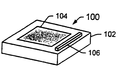
FIG. 1 is a perspective view of a hybrid radiation
imaging chip that includes both CCD and CMOS components.
CA 02355307 2001-06-18
WO 00/38217 PCT/US99/29653
FIG. 2 is a schematic diagram of a hybrid radiation
imaging chip that includes both CCD and CMOS components.
FIG. 3 is a flow chart of a process for fabricating
a hybrid. radiation imaging chip using both CCD and CMOS
5 processes.
FIG. 4 is a schematic diagram of another hybrid
radiation imaging <:hip that includes both CCD and CMOS
components.
FIG. 5 is a f7_ow chart of a process for calibrating
a hybrid imaging chip .
Detailed Description
FIG. 1 shows a perspective view of a hybrid CCD-CMOS
imaging chip 100. The imaging chip includes a substrate
102 that has a CCD array 104 formed on one surface by a
conventional CCD fabrication process, such as a buried
channel or perista7_tic process. A conventional CCD
device includes a buried-channel amplifier in the CCD
substrate that converts charge collected in the CCD array
into voltage-mode signals. The CCD portion of the hybrid
chip 100 does not include such an amplifier.
A CMOS-based clam stage is formed on another
substrate 106 by a conventional CMOS fabrication process.
CA 02355307 2001-06-18
WO 00/38217 PCT/US99/29653
6
This gain stage replaces the buried-channel amplifier
normally formed on a CCD chip. As described below, the
two substrates 102, 106 are bonded together after the CCD
and CMOS circuits are formed. This eliminates any need
to integrate the CC'D and CMOS fabrication processes
together. In many implementations, signal processing
electronics can be formed on the CMOS substrate 106 to
provide full imaging capability on the hybrid chip 100.
FIG. 2 shows a block diagram of the hybrid imaging
chip 100. The CCD substrate 102 includes individual
detector elements :115A-L, or "pixels," arranged as a CCD
array 104. As in a conventional CCD imaging device, the
array 104 includes one or more lines 110A-D (rows or
columns) of CCDs coupled to a high-speed serial register
112. Upon exposure to electromagnetic radiation, the
pixels 7.15A-L collect charge in capacitively coupled
potential wells formed in a semiconductor layer, such as
an epitaxial silicon layer. Optically transparent
control gates formed on the image area hold the collected
charge :i.n the potential wells. The pixels 115A-L
transfe:r the collected charge along the lines 110A-D to
the high-speed serial register 112 in response to a
series of pulses applied to the control gates.
CA 02355307 2001-06-18
WO 00/38217 PCT/US99/29653
7
The high-speed serial register 112 on the CCD
substrate 102 is coupled to a CMOS charge-mode amplifier
114 formed on the CMOS substrate 106. In one
implementation, the charge-mode amplifier 114 is an
operational amplifier configured as a charge integrator.
This amplifier 114 can lower the noise during charge
collection. Because the CMOS charge-mode amplifier 114
is not formed on th.e substrate 102 on which the imaging
array 104 is formed., the amplifier 114 is not subject to
size constraints. As a result, the amplifier 114 can
include components that are sized to yield optimum 1/f
and thermal noise performance. Thus, the amplifier 114
can outperform amplifiers found in conventional CMOS
imaging devices, such as CID and APS devices. Because
the amplifier 114 i.s a CMOS device, it also consumes very
little power, typically an order of magnitude less than
conventional CCD amplifiers.
In some implementations, the CMOS substrate 106 also
includes CMOS signal processing circuitry, such as a
double-sampling c.iz-cuit 116, an analog-to-digital
converter (ADC) llf3, and a digital signal processor (DSP)
120. These components provide noise reduction and image
processing capability on the hybrid imaging chip 100.
CA 02355307 2001-06-18
WO 00/38217 PCT/US99/29653
8
The CMO~~ substrate 106 also includes timing and control
circuitry 122 that controls the transfer of charge from
the pixels 115A-L :in the array 104 to the high-speed
serial register 112. In a conventional CCD imaging
device, the timing and control circuitry is often formed
on a set>arate chip .
In some implementations, the CCD and CMOS components
are coupled by electrically conductive pads 124A-F formed
on the C'CD substrate 102 and the CMOS substrate 106.
These pads 124A-F are aligned to allow mechanical and
electrical interconnection of the substrates 102, 106. A
conventional flip-chip technique using an infrared (IR)
microscope and alignment marks on the CCD and CMOS
substrates can be used to align the substrates.
FIG. 3 illustrates an overview of a technique for
fabricating the hybrid imaging chip 100. The imaging
array is: formed on one substrate using a conventional CCD
fabrication procesa, such as the buried channel and
peristaltic CCD fabrication processes (step 130).
Likewise, the charge-mode amplifier, the signal
processing circuitry, and the timing and control
circuitry are formed on another substrate using a
conventional CMOS :Fabrication process (step 132).
CA 02355307 2001-06-18
WO 00/38217 PCT/US99/29653
9
Bonding pads are formed on each substrate during these
fabricat:ion processes. The fabrication processes are
optimized individually to produce circuits capable of the
highest performance quality.
, Once the substrates have been fabricated, a bonding
material is placed on the bonding pads (step 134), and
the CMO~~ substrate is positioned on the CCD substrate
(step 136). The two substrates are then bonded together
using any of a variety of techniques (step 138).
l0 Examples of such techniques include conventional bump-
bonding techniques.
FIG~~. 4 shows another structure for a hybrid CCD-CMOS
imaging chip 150. This imaging chip 150 includes a non-
destructive sense node 152A-D, implemented in this
example as a float_Lng polysilicon gate, for each line
154A-D in the CCD array 156. These sense nodes 152A-D
replace the usual high-speed serial register. The non-
destructive sense nodes 152A-D are typically formed on
the CCD substrate 155 and operate as described below.
The imaging chip 150 includes CMOS charge-mode
amplifiers 158A-D formed on the CMOS substrate 165. Each
is coupled to one of the non-destructive sense nodes
152A-D. Each of the amplifiers 158A-D also is coupled to
CA 02355307 2001-06-18
WO 00/38217 PCT/US99/Z9653
a corresponding averaging circuit 160A-D. In many
implementations, a double-sampling circuit 164A-D is
formed between each pair of amplifiers 158A-D and
averaging circuits 160A-D.
5 A high-speed C'MOS multiplexes 162 receives voltage-
mode signals from t:he averaging circuits 160A-D and
delivers a single signal to an analog-to-digital
converter (ADC) 16E~. The ADC 166 digitizes the signal
and delivers it to a digital signal processor (DSP) 168.
10 A look-u;p table 179: is stored in a storage device, such
as a writable read-only memory (ROM) device, for use by
the DSP 168, as described below.
A timing and control circuit 170 on the CMOS
substrate 165 delivers control signals to the CCD array
156, the non-destructive sense nodes 152A-D, the
averaging circuits 160A-D, and the CMOS multiplexes 162.
Optional bonding pads 172A-J are formed on the CCD and
CMOS substrates 155, 165 to allow mechanical and
electrical interconnection between the substrates.
The non-destructive sense nodes 152A-D, the CMOS
amplifiers 158A-D, and the averaging circuits 160A-D
together provide parallel channels for converting the
charge collected in each of the lines 154A-D of the CCD
CA 02355307 2001-06-18
WO 00/38217 PCT/US99/29653
11
array 156. In general, the CCD array 156 is capable of
transferring charges at a rate much higher than that
required in scientific applications. For example, a
typical application might require transferring data from
a 128 x 128 array t:o the signal processing circuitry at
an effective rate c>f 10 frames per second, or 1.28 kHz
per line. A typical CCD array, however, can support a
much higher line transfer rate, e.g., 128 kHz.
Therefore, the CCD array 156 in this example can support
100 samples from each detector in the array 156 between
each transfer to the digital signal processor 168.
Since the sen~oe nodes 152A-D are non-destructive,
the charge in those nodes can be repeatedly measured.
The averaging circuits 160A-D connected to the CMOS
i5 amplifiers 158A-D average or accumulate the samples
measured during successive sampling periods of, for
example, 100 samples. At the end of each sampling
period, the averaging circuits 160A-D deliver the stored
charge to the high-speed multiplexer 162.
This type of parallel charge measurement reduces
readout noise by a factor approximately equivalent to the
square root of the number of samples taken for each
pixel. For a 128 }: 128 array operating at a transfer
CA 02355307 2001-06-18
WO 00/38217 PCT/US99/29653
12
rate of 10 frames per second, readout noise is reduced
from approximately 4 electrons rms to approximately 0.4
electrons rms.
FIG. 5 illustrates a technique for use in
calibrating the parallel hybrid imaging chip 150 of FIG.
4 to improve image quality. In general, this technique
allows for correction of column-to-column offset and gain
variations that often result from minor differences in
CMOS amplifier geometries. This technique is carried out
in the digital signal processor 168 (FIG. 4) or in other
processing circuitzy, such as a programmable processor,
in the imaging chip or another chip.
The signal processing circuitry first reads all or a
portion of a uniform image, such as a dark current
generated by pixel; in an optically opaque portion of the
imaging field (step 180). The DSP or other processing
circuitry calculates an average image value in the
uniform image (step 182). For each line in the array, a
variance between the measured charge and the average
value is calculated (step 184). The processing circuitry
normalizes the variances (step 186). The normalized
variances represent: the amount of gain variation among
CA 02355307 2001-06-18
WO 00/38217 PCT/US99/29653
13
the CM03 amplifiers. These normalized variances are
stored in the look-up table described above (step 188).
The' processing circuitry retrieves and applies the
normalized variances during normal operation of the
imaging chip (step 190). In general, applying the
normalized variances involves multiplying the values
stored in the look-up table with the real-time
measurements of corresponding pixels in the array.
Normalizing the measured values in this manner eliminates
the effects of gain variations among the amplifiers.
Then invention has been described in terms of
particular embodiments. Various modifications can be
made without departing from the spirit and scope of the
invention. For example, while the invention has been
described in terms of photon detection and imaging, it is
also useful in detecting and imaging other types of
radiation, including charged particles. Also, the
imaging circuit often varies among implementations. For
example,. some implementations do not include dedicated
averaging circuits for each line of the array, but rather
implement the averaging function in the digital signal
processor 168 (FIG. 4). Likewise, other types of
capacit:ively coupled detectors, such as "bucket-brigade"
CA 02355307 2001-06-18
WO 00/38217 PCT/US99/29653
14
detectors implemented with bipolar junction transistors,
can be used. Also,, while electrical connection between
the substrates is described, other forms of signal
coupling, such as optical coupling, is contemplated.
Accordingly, other embodiments are within the scope of
the following claims.