Note: Descriptions are shown in the official language in which they were submitted.
CA 02355450 2001-08-20
71493-1006
1
HYBRID ATTACH MIRRORS FOR A MEMS OPTICAL SWITCH
Field of Invention
The invention relates to an improved method of
manufacturing an array of parallel mirrors, in particular an
array of mirrors to be secured on an array of actuators to
function as a MEMS (micro electromechanical systems) optical
switch.
Background
MEMS optical switches are well known in the art.
One variation of these optical switches comprises a series of
actuators each having a mirror secured thereto. The
actuators move the mirror in and out of the line of travel of
an input signal light beam to selectively reflect the light
beam to an output.
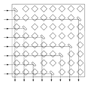
The MEMS optical switches that comprise a series of
mirrors secured to actuators are often arranged in an m x n
array to redirect m input light beams to one of the n
outputs. Figure 1 is a typical 8 x 8 array used for
telecommunications switch applications. As is shown in the
figure, 8 of the 64 actuators are in an on position where the
mirror is placed within the direction of travel of one of the
input light beams thereby redirecting each of the light beams
to one of the outputs. The remaining 56 of the actuators are
in an off position where the mirror is positioned out of the
line of travel of the input or redirected light beams. An
array of the type shown in Figure 1 would be approximately 1
cm X 1 cm in size with a space between each input light beam
of approximately 1 mm. Due to the size of these switches,
there are very strict tolerances on the mutual alignment of
the input light beams as well as the redirecting accuracy of
CA 02355450 2001-08-20
71493-1006
2
the mirrors. Each mirror must be set to reflect the light
beam by precisely the same angle, typically 90 degrees,
because slight variations can negatively impact the operation
of the device.
It is virtually impossible to assemble these arrays
of actuators and mirrors with the required accuracy by
affixing the mirrors to the actuators one at a time by hand
or through automation. In the field of surface micro
machining, there are several methods of fabricating mirrors
from the same material used to fabricate the actuators. These
techniques can result in the required accuracy in location
and orientation of the mirrors. In one such method the
mirror is etched from layers of polycrystalline silicon
during the same etching step used to fabricate an actuator.
In this process, the mirrors are etched in a plane parallel
to that of the actuator and then flipped up to a vertical
position. However, the mirrors fabricated using this process
have reflective surfaces that are rough. A rough mirror
causes the reflected light beam to scatter as it travels away
from the mirror thereby resulting in losses in the switch.
Further, the mirrors fabricated using this technique are
typically thin and are coated with gold or titanium tungsten
and gold to form a reflective surface. As a result, a
thermal bimorph between the gold and the underlying material
exists due to the high temperature at which the gold is
deposited along with the subsequent contraction when the
mirror is cooled to room temperature as well as the
difference in thermal expansion of the gold and the
underlying material. Thus, as the ambient temperature around
the mirror changes, there is an increase or decrease in the
stress between the gold and the underlying material that
results in curvatures in the reflective surface of the
mirrors. A curvature in the mirror will result in expansion
CA 02355450 2001-08-20
71493-1006
3
or contraction of the reflected light thereby resulting in
losses in the switch.
A second technique used is to fabricate an array of
mirrors and actuators is the fabrication of each element from
the same wafer of crystalline silicon material. The mirrors
are fabricated in a vertical plane using a first etching
process and then the actuators are fabricated from silicon
material positioned under the mirrors using a second etching
process. However, the mirrors known in the art fabricated
using this process are rough thereby resulting in losses in
the switch. In addition, the actuators fabricated using this
technique require a substantial large surface area of
material and accordingly, the spacing between the mirrors is
significantly larger compared to the spacing of mirrors
fabricated using other techniques. As a result, the array of
actuators and mirrors fabricated using this technique is
significantly larger in size than arrays fabricated using
other techniques.
Summary of Invention
It is an object of the present invention to provide
a novel method of constructing an array of parallel mirrors
for attachment to an array of actuators to be used as a MEMS
optical switch.
According to one aspect of the invention, there is
provided a method of manufacturing an m x n array of mirrors.
A substrate is attached to a bottom surface of a crystalline
material having an upper surface and a series of parallel
crystal planes perpendicular to the upper surface. A set of
channels are then etched in the crystal material defining an
m x n array of columns, each column having two parallel flat
sides formed from one of the parallel crystal planes of the
CA 02355450 2001-08-20
71493-1006
4
crystalline material. The columns are then coated with a
reflective material thereby providing a flat reflective
surface .
According to another aspect of the invention, there
is provided a method of manufacturing an optical switch
comprising an m x n array of mirrors mounted on actuators.
An m x n array of columnar mirrors is provided, the array
being formed from a single piece of crystalline material.
The crystalline material has upper surface and a series of
l0 parallel crystal planes perpendicular to the upper surface.
Each mirror in the array has two parallel flat sides formed
from one of the parallel crystal planes and is coated with a
reflective material. The lower end of each. mirror is secured
to a mirror substrate . An m x n array of actuators is then
fabricated on an actuator substrate and aligned with the
array of mirrors such that the parallel flat sides of each of
the mirrors are positioned in a predetermined orientation
relative a corresponding actuator on the actuator substrate.
The mirrors are then secured to the corresponding actuator on
the actuator substrate in the predetermined orientation.
Once secured to the actuators, the mirrors are then released
from the mirror substrate thereby permitting the mirrors to
move relative to each other.
According to yet another aspect of the invention,
there is provided an m x n array of mirrors. The array is
formed from a single piece of crystalline material having an
upper surface and a series of parallel crystal planes
perpendicular to the upper surface. Each mirror in the array
has two parallel flat sides formed from one of the parallel
crystal planes of the crystalline material. The mirrors are
coated with a reflective material and have a lower end
secured to a substrate.
CA 02355450 2001-08-20
71493-1006
Brief Description of the Drawings
Preferred embodiments of the invention will now be
described by way of example with reference to the attached
drawings in which:
5 Figure 1 is a top view to an enlarged scale of a
schematic drawing of an array of mirrors secured to an array
of actuators of the type known in the art;
Figure 2 is a corner side view to an enlarged scale
of two silicon wafers adhered together prior to a first
etching process in accordance with an embodiment of the
invention;
Figure 3 is a corner side view of the two silicon
wafers shown in Figure 2 with masking layers placed thereon;
Figure 4 is a corner side view of the two silicon
wafers shown in Figure 2 after the first etching process is
completed in accordance with an embodiment of the invention;
Figure 5 is a perspective view of the two silicon
wafers shown in Figure 4;
Figure 6 is a front cross-sectional view of the two
silicon wafers shown in Figure 4 along line 6-6;
Figure 7 is a front cross sectional view of the two
silicon wafers shown in Figure 6 after a set of columns of
silicon material are etched out of the first silicon wafer
after a second etching process has been completed in
accordance with an embodiment of the invention;
Figure 8 is a perspective view of the set of
columns shown in Figure 7;
CA 02355450 2001-08-20
71493-1006
6
Figure 9 is a front cross-sectional view to an
enlarged scale of a set of mirrors in accordance with an
embodiment of the invention;
Figure 10 is a front cross-sectional view of the
set of mirrors shown in Figure 9 inverted above an actuator
substrate in accordance with an embodiment of the invention;
Figure 11 is a front cross-sectional view of the
set of mirrors and actuator substrate shown in Figure 10
wherein the mirrors have been moved into contact with and
bonded to actuators on the actuator substrate in accordance
with an embodiment of the invention;
Figure 12 is a front cross-sectional view of a
completed array of actuators with mirrors attached thereto
manufactured in accordance with an embodiment of the
invention;
Figure 13 is a side view to an enlarged scale of a
cantilever actuator with a mirror on the end thereof of a
type known in the art, the actuator being in an up position;
and
Figure 14 is a side view of the cantilever actuator
shown in Figure 13 in a down position.
Detailed Description of Preferred Embodiments
A method of fabricating an optical switch
comprising an array of flat, parallel mirrors in accordance
with an embodiment of the invention is illustrated in Figures
2 to 9. In addition, a method of attaching the array of
mirrors to an array of actuators to fabricate an optical
switch of the type shown in Figure 1 in accordance with
CA 02355450 2001-08-20
71493-1006
7
another embodiment of the invention is illustrated in Figures
to 12.
According to an embodiment of the invention, the
method of fabricating an optical switch comprising an array
5 of mirrors secured to actuators comprises three main steps of
fabricating an array of mirrors attached to a substrate, as
shown in Figures 2 to 9, attaching the mirrors to an array of
actuators as shown in Figures 10 & 11 and releasing the
mirrors from the substrate as shown in Figure 12.
l0 With reference to Figure 2, a first silicon wafer 1
is secured to a second silicon wafer 3 by an adhesive layer
of silicon dioxide 5. The first silicon wafer 1 has a
crystal orientation <110> whereas the second silicon wafer
can have any crystal orientation. Typically, the standard
<100> crystal orientation of silicon will be used for the
second silicon wafer. There are many known ways of
assembling two silicon wafers in this manner. Typically, the
silicon dioxide is deposited on one or both of silicon wafers
that are then pressed together in a controlled atmosphere at
high temperature and pressure. It is possible to purchase
prefabricated <110> silicon wafers already attached to
standard <100> wafer by a layer of silicon dioxide.
The choice of the vertical thickness of the first
silicon wafer 1 will depend upon the application for which
the mirrors will be used. The thickness can range from 10's
of microns to 300 - 400 microns. The second silicon wafer 3
must be of a sufficient thickness that it is mechanically
robust so that it can be manipulated through the various
steps in the procedure. Typically a thickness in the order
of 400 microns is sufficient. The layer of silicon dioxide 5
can have a thickness ranging from 0.1 to 2 microns.
CA 02355450 2001-08-20
71493-1006
8
As shown in Figure 3, a set of masking layers 7 are
positioned on the upper surface of the first silicon wafer 1.
The masking layers 7 preferably have two layers 8 and l0 of
different material. The masking layers 7 have a width of
typically 20 to 50 microns and extend across the first
silicon wafer 1. The materials forming the masking layers 7
are deposited onto the silicon wafer 1 and patterned using
techniques well know in the art such that masking layers 7
are positioned parallel to each other and typically having a
l0 spacing of approximately 1 mm. Due to the fact that the
upper wafer has a <110> crystalline orientation, the <111>
planes are perpendicular to the wafer surface. The masking
layers 7 are positioned such that they are parallel to the
<111> crystal plane of the first silicon wafer 1. The
alignment of the masking layers with the <111> planes is
accomplished by a reference etch that is marked on the <110>
silicon wafer during an alignment step which is well known in
the art.
The first silicon wafer 1 is then subjected to a
two step etching process. The first etching step creates a
set of parallel rows of silicon by etching a set of channels.
The results of this etching step are shown in Figures 4 to 6.
The second etching step divides each of the rows into a
series of silicon columns as illustrated in Figures 7 and 8.
The first etching process is a wet etch. The
etchant used is of the type that does not etch the <111>
planes of the silicon wafer. Potassium hydroxide is an
example of such etchant.
With reference to Figures 4, 5 and 6, the wet
etching process creates channels 9 in the portions of the
first silicon wafer 1 not protected by the masking layers 7
CA 02355450 2001-08-20
71493-1006
9
thereby creating a set of parallel rows 11 in the silicon
wafer. Due to the fact that the <111> planes are
perpendicular to wafer surface, the etch results in side
walls 13 of the rows 11 which are very smooth and absolutely
flat. Further, the etchants used do not etch silicon
dioxide. Accordingly, this process does not etch into the
adhesive layer of silicon dioxide 5.
In addition, as shown in Figure 6, due to the two
layers 8 and 10 of different materials in the masking layers
l0 7, the first etching process removes the first layer 8 from
the masking layers 7 thereby exposing the second layer 10 of
the masking layers which is the same width but have spaces 12
positioned over the length thereof thereby exposing the
surface of portions of the rows 11. The use of two masking
layers for a two step etching process is well known in the
art.
With reference to Figure 7 and 8, a second etching
step is conducted wherein the rows 11 are divided into a
series of individual columns. The end walls 17 of the
columns 14 created by this second etching process do not need
to be as precise in terms of verticality or roughness as the
side walls 13 created by the first etching process.
Accordingly, the second etching process does not need to be
the wet etching process used in the first etching step. One
possible etching technique which can be used is Deep Reactive
Ion Etching (DRIE) which provides very high etch rates and
nearly vertical walls. As with the wet etch, the chemistry
of the DRIE technique does not etch the silicon dioxide
adhesive layer 5. Other suitable etching techniques are
known by those skilled in the art. Upon completion of the
second etching process, the layer 10 of the masking layers 7
is removed from the columns 14.
CA 02355450 2001-08-20
71493-1006
As shown in Figure 9, the final step in the
fabrication of the array of mirrors is completed by forming a
metal coating on each of the columns 14 using standard
metalization techniques, i.e. sputtering, to form an array of
5 mirrors 15. With appropriate lithography (i.e. coarse
features) it is possible to pattern the metal deposited on
the adhesive layer of silicon dioxide 5 thereby allowing the
silicon dioxide layer to be exposed for the purpose of the
releasing etching step describe hereinafter. A preferred
l0 metalization is a thin layer of titanium tungsten with a
coating of gold on the top thereof. The reflectivity of gold
in the infrared, the region of the spectrum where
telecommunications systems are designed, is above 97%.
Further, gold does not oxidize, making it a good candidate
for the soldering operations described hereinafter. The
metal layer can be deposited on only one of the flat sides of
the columns 14 or preferably, the entirety of columns 14 can
be coated with the metal layer.
The mirrors 15 created by the process not only have
flat, smooth, parallel reflective surfaces when manufactured,
they remain flat over a greater range of temperatures than
conventional mirrors. The thickness of the mirrors 15
created by this process are in the order of 20 to 50 microns
whereas some of the conventional mirrors structures have a
thickness in the order of 2 microns. Accordingly, the
mirrors 15 are stronger than the conventional mirrors and
thus less susceptible to deflections. Further, mirrors 15
that are coated on both sides have the benefit of the
stresses caused by the thermal bimorph are the same on both
sides thereby acting against each other and significantly
reducing any resulting deflections of the mirror surface.
CA 02355450 2001-08-20
71493-1006
11
Once the array of mirrors is fabricated, if
desired, the mirrors 15 can be attached to an array of
actuators. The method employed to attach the mirrors 15 is a
"flip chip" bonding method well known in the art and which
can take many forms. As shown in Figure 10, the second
silicon wafer 3 and the mirrors 15 are flipped upside down
and positioned in a flip chip apparatus above an actuator
substrate 19. The actuator substrate 19 has an array of
actuators thereon which are manufactured using one of several
known techniques. A typical cantilever actuator known in the
art is shown in Figures 13 and 14. As illustrated in Figure
13, a flap 30 of the polycrystalline silicon is etched from
the substrate 19 thereby releasing free end 34 of the flap 30
from the substrate. An opposing end 32 of the flap 30 is
anchored to the substrate 19. A layer of stressed metal
(i.e. gold) is deposited on the top of the flap. The stress
of the metal tends to pull the free end 34 of the flap 30 off
the surface of the substrate 19 and curl it towards the fixed
end 32 of the flap. By controlling the thickness of the flap
30 and the metal layer, the deposition conditions and the
length of the flap, differing amounts of curl can be
produced. As shown in Figure 14, the free end 34 of the flap
is forced back down onto the substrate 19 by the
application of a DC voltage. The electrostatic force created
25 by the voltage will cause the flap 30 to uncurl and lie down
flat on the substrate 19. In this position, a mirror 36
secured to the free end 34 of the flap 30 is positioned in
the path of travel of a light beam, thereby redirecting the
light beam. Once the voltage is removed, the flap 30 will
30 curl up again to the position shown in Figure 13.
The spacing between the mirrors 15 and the
actuators on the actuator substrate 19 is set such that each
of the mirrors can be placed in alignment with and above an
CA 02355450 2001-08-20
71493-1006
12
actuator on the actuator substrate 19 during the flip clip
process. As the manufacturing process of the mirrors ensures
that each of the flat parallel surfaces 13 of the mirrors 15
are parallel, the orientation of each of the mirrors is
identical relative to the actuators once the mirrors are
positioned in alignment with the actuators.
As shown in Figures 10 and 11, the mirrors 15 are
attached to the actuators on the actuator substrate 19 by
soldering the mirrors to the actuators. A solder patch 21 is
positioned on each actuator in a predetermined position. The
mirrors 15 are positioned above the actuator substrate 19 and
are aligned with the solder patch 21 to ensure the correct
orientation. With reference to Figure 11, the mirrors 15 are
then brought into contact with the solder patches 21 and the
solder patches are melted to attach the mirrors to the
actuators. The heating process to melt the solder preferably
includes gentle temperature ramps in order to minimize
thermal shock. The heating process may also consist of a two
step process whereby the first heating process is conducted
when the mirrors 15 are first brought into contact with the
solder 21 such that solder becomes soft and has sufficient
adhesion to hold the mirrors 15. The actuator substrate 19
and mirrors 15 are then removed from the apparatus used to
align the mirrors and put into an oven which is heated to
complete the melting and alloying process of the solder
patches 21.
The solder patches can comprise many different
types of solders. Gold solder could be used which results in
a simple metal to metal bond with only heat and pressure.
Alternatively, eutectic bonding could be used with a fluxless
solder, such as Au-Sn, which bonds well in a controlled
atmosphere. Alternatively, eutectic or non-eutectic solders,
CA 02355450 2001-08-20
71493-1006
13
such as Pb-Sn or Pb-Ag may be used which may or may not
require flux or a controlled environment.
During the alloying process, stresses in the solder
tend to build up. However, due to the fact that the mirrors
are maintained in attachment to the second silicon wafer 3, a
post-alloy anneal can be conducted to reduce the stress
thereby reducing the possibility of distortion in the mirrors
or the actuators due to the soldering process.
It would be understood by those skilled in the art
that the use of one or multiple solder patches for attachment
of each mirror to an actuator on the actuator substrate 19 is
dependant on the structure of the underlying actuator. A
continuous strip of solder running the entire length of the
mirror might cause undue stress on some forms of thin
actuators causing the actuator to deflect. Using two half
length strips of solder as opposed to one can reduce the
stress. It would also be understood by those skilled in the
art that the mirrors could be attached to the actuators by
means other than soldering, including the use of a polymer
bond or epoxy.
The final step in the manufacturing process is the
removal of the adhesive layer of silicon dioxide 5 thereby
permitting the second silicon wafer 3 to be removed to
release the mirrors 15 as is shown in Figure 12. The
adhesive layer of silicon dioxide 5 is removed by exposing
the layer to an etchant that dissolves the layer thereby
releasing the mirrors 15. Hydrofluoric acid or buffered
oxide etch are examples of etchants which can be used for
this process. Due to the relatively small space (typically
less than 2 microns) that the etchant has to enter between
CA 02355450 2001-08-20
71493-1006
14
the two silicon wafers 1 and 3, this etching process is slow
and controlled.
As it is preferable to have the actuators secured
to the actuator substrate 19 during the bonding of the
mirrors, the last step of releasing the actuators from the
actuator substrate 19 is not completed prior to attaching the
mirrors to the actuators. Accordingly, the final step of
removing the adhesive layer 5 may also include the last
etching step in the fabrication of the actuators such that
the actuators are released from the actuator substrate 19.
As noted above, the orientation of the mirrors is
crucial for MEMS optical switches. Due to the fact that the
mirrors are maintained within the crystallographic
orientations of the original silicon wafer during the entire
bonding process, uniform orientation is assured.
Although the description above has referred to the
first silicon wafer having a <110> crystalline orientation
and the flat parallel surfaces of the mirrors 15 being formed
from the <111> crystal planes, it will be understood by those
skilled in the art that any crystalline material with
parallel crystal planes perpendicular to a surface of the
material could be used. Further, an etchant must also be
available to selectively etch the crystalline material such
that the etchant does not etch through the parallel crystal
planes. In addition, a person skilled in the art will
understand that the adhesive layer of silicon dioxide could
be replaced by other forms of adhesive which can be removed
during the process of releasing the mirrors by an etchant or
other known techniques.
It will be understood by those skilled in the art
that numerous alterations, modifications and variations to
CA 02355450 2001-08-20
71493-1006
the above embodiments can be made without departing from the
substance of the invention.