Note: Descriptions are shown in the official language in which they were submitted.
CA 02355719 2001-06-20
WO 00/38345 PCT/SE99/02399
ECHO A11'D DISTORTION CANCELLATION ARRANGEt\'(ENT
TECHNICAL FIELD
The invention relates generally to line drivers and more specifically to an
echo and
distortion cancellation arrangement in line drivers.
BAChGROUNI) OF THE INVENTION
In a line driver connected to a telephone line for tuansmitting signals
generated by a
signal source and receiving signals incoming on the n~ansmission line, echoes
and
distortions caused by the line driver itself as well as by the signal source
appear to-
gether with the signals to be transmitted and the signals to be received
across the
output terminals of the line driver.
With long transmission lines, the received signals are only fractions of the
trans-
miffed signals at the line driver output.
SUMMARY OF THE INVENTION
The object of the invention is to reduce such echoes and distortions in the
Feceive
path of the line driver.
This is attained in accordance with the invention by providing an additional
driver
for driving a separate load with the same voltages and cuwents in its signal
path as
the "normal" line driver.
The additional driver is, thus, not affected by signals received on the
telephone line
since it, instead, is connected to that separate load.
Thus, the additional driver miwors the signal to be transmitted by the
"normal" line
driver with the same distortion and signal levels to the separate load.
CA 02355719 2001-06-20
WO 00/38345 PCT/SE99/02399
2
By subtracting the signal on the telephone line, which includes both the lar'e
trans-
mitted signal with its related distorrtion and the often small received
signal, from the
signal "transmitted" to the separate load by the additional driver, which only
in-
cludes the large transmitted signal and its related distortion, the difference
will ide-
s ally be the signal' received on the telephone line, reduced from the
h~ansmitted signal
as well as the transmitted distortion and noise.
Since the transmitted signal has the same currents and voltages in the signal
path
through both the "normal" lire driver and the additional driver, and both the
line
driver and the additional driver are preferably fabricated on the same die,
the differ-
ence in distortion and voltage levels of the transmitted signals will be
minimized.
BRIEF DESCRTPTION OF T'HE DRAWING
The invention will be described more in detail below with reference to the
appended
drawing on which Fig. I illustrates a known line driver with a first
embodiment of
an arrangement according to the invention, Figs. 2a, 2b and 2c are signal
diagrams
illustrating different signals in the embodiment in Fig. I, Fib. 3 illustrates
another
known line driver with a second embodiment of an awangement according to the
in-
vention, and Fig. 4 illustrates a further known line drrver with a third
embodiment
of an arrangement according to the invention.
DESCRIPTION OF THE INVENTION
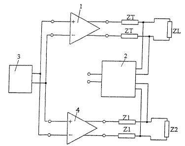
Fig. I shows a known line driver 1 with a first embodiment of an echo and
distor-
tion cancellation arrangement in accordance with the invention.
In a manner known per se, the known line driver 1 has two input terminals and
two
output terminals.
In the embodiment in Fig. I, the output ter-rninals of the line driver 1 are
connected
via terminating impedances Z'T to respective wire of a two-wire taansrnission
line as
CA 02355719 2001-06-20
WO 00/38345 PCT/SE99/02399
3
well as to input terminals of receivin~~ means ? for receiving signals
incoming on the
transmission line. A line impedance of the tl'a11S1111SS1011 line is denoted
ZL in Fig. 1.
The input terminals of the line driver 1 are connected to output telirlinals
of a signal
source 3 for generating output signals to be transmitted on the transmission
line.
The output signals of the line driver 1 on the transmission line, emanating
from the
signal source 3, are superimposed on signals coming in to the line driver 1 on
the
transmission line to be received by the receiving means ? for ful-ther
processing. The
receiving means ? is connected with its output terminals to signal processing
means,
e.g. an analog-to-digital converter (not shown).
The output signals of the line driver 1 on the tl'ansnllSSlol1 line, i.e. the
transmitted
signals, are accompanied by distol-tion and noise generated by the line driver
1 itself
as well as by the signal source 3.
At the output terminals of the line driver I, the output signals are large.
At the same time, signals coming in to the line driver 1 on the transmission
line, i.e.
the received signals, are small in comparison with the h~ansmitted signals.
Fig. 2a schematically illustrates the power spectral density (PSD) in dBm
versus
frequency f of the signals at tire output of the line driver 1 in Fig. 1
towards the
transmission line.
The transmitted signal is represented by solid lines, the distortion
associated with
the transmitted sil;nal is represented by dotted lines, and the received
signal is repre-
sented by dashed lines.
As apparent from Fig. 2a, the distortion may be of the same level as the
received
signal.
CA 02355719 2001-06-20
WO 00/38345 PCT/SE99/02399
4
In accordance with the invention, to cancel echo and distortion that appear
across
the output terminals of the line driver l, an echo and distortion cancellation
ar-
rangement in the form of a modified version of the known line driver described
above, is added to the known line driver 1 to cooperate therewith.
The echo and distortion cancellation art-angement according to the invention,
i.e. the
additional driver 4 also has two input terminals and two output terminals.
The output terminals of the additional driver 4 are connected via impedances Z
1
across a load Z2 as well as to additional input terminals of the receiving
means 2.
The input terminals of the additional driver 4 are connected to the output
terminals
of the signal source 3 for generating the same sil;nals across the load Z2 as
gener-
ated by the line driver 1 across the telephone line.
Fig. 2b schematically illustrates the signals at the output of the additional
driver 4
towards the load Z2.
The signal transmitted to the load Z2 is represented by solid lanes, and the
distortion
associated with that signal is represented by dotted lines.
As apparent, the signals transmitted on the telephone line and to the load Z2
as il-
lustrated in Figs. a!a and 2b, respectively, as well as the distortion
associated with
these signals, are the same.
In accordance with the invention, the receiving means 2 is adapted to
subri~act the
signal generated across the load Z2 as illusti~ated in Fig. 2b from the
signals on the
transmission line as illusri~ated in Fig. 2a in order to cancel the t1-
ansmitted signal
with its distortion and noise from the incoming signal on the tz~ansmission
line.
CA 02355719 2001-06-20
WO 00/38345 PCT/SE99/02399
This is schematically illustaated in Fig. 2c in which only the received signal
remains
after the subh~action by the receiving means 2. In practice, it is however to
be under-
stood that a portion of the transmitted signal as well as a portion of its
associated
distortion also can remain after the subtuaction.
5
In accordance with the invention, to reduce the power consumption of the
additional
driver 4, the impedances Z1 are of an impedance value that is k times the
impedance
value of the terminating impedances ZT, k being an integer. Also, the
impedance
value of the load Z2 is k times the impedance between the output terminals of
the
line driver I.
Also, in accordance with the invention, the size of the output transistors
(not shown)
of the additional driver 4 is 1/k times the size of the output transistors
(not shown)
of the line driver 1.
The reason for scaling the output transistors in the additional driver 4 is to
achieve
the same current density in both the "normal" line driver 1 and the additional
driver
4 in order to get the same distortion.
Hereby, echoes and distortions will be efficiently canceled from the input
signals on
the transmission line to be received by sil;nal processinb means (not shown)
con-
nected to the output terminals of the receiving means 2.
Fig. 3 shows another embodiment of a known line driver 5 with a second embodi-
ment of an echo and distorrtion cancellation arrangement in accordance with
the in-
vention.
In a manner known per se, the known line driver ~ in Fig. ~ lras two input
terminals
and two output terminals.
CA 02355719 2001-06-20
W,O 00/38345 PCT/SE99/02399
6
In the same manner as described above in connection with Fig. 1, the output
termi-
nals of the line driver 5 are connected to respective wire of a tw°o-
wire transmission
line as well as two input terminals of a receiving means 6 for receiving
signals in-
coming on the transmission line. In Fig. 3, the transmission line has a line
imped-
ance Z3.
The input terirrinals of the line driver 5 are connected to output ter-rninals
of a signal
source 7 for generating output signals to be n~ansrnitted on the transmission
line.
The input terTrrinals of the line driver S are also connected in a manner
known per se
to output terminals of a cuwent-to-voltage converter 8 which is connected with
its
input terzrrinals to the wires of the transmission line.
The line driver output signals on the transmission line, emanating from the
signal
source 7, are superimposed on signals coming in to the line driver 5 on the
transmis-
sion line to be received by the receiving means 6 for further processing. The
re-
ceiving means 6 is connected with its output terminals to signal processing
means,
e.g. an analog-to-digital converter (not shown).
The line driver output signals on the transmission line, i.e, the tuansmitted
signals,
are accompanied by distortion and noise generated i.a. by the signal source 7.
As described above in connection with Fig. 1, the output signals at the output
termi-
nals of the line driver ~ are large, while incoming signals to the line driver
~ on the
transmission line, i.e. the received signals, are small in comparison with the
trans-
miffed signals.
Also in the line driver 5 in Fig. 3, the power spectral density, PSD, versus
fre-
quency, f, of the signals at the output of the line driver 5 will be as
illustrated in Fig.
2a.
CA 02355719 2001-06-20
WO 00/38345 PCT/SE99/02399
7
Also in the embodiment in accordance with Fig. 3, to cancel echo and
distorrtion that
appear across the output terminals of the line driver 5, an echo and
distortion can-
cellation arrangement in the fomn of a modified version of the known line
driver 5
described above, is added to the known line driver 5 to cooperate therewith.
The echo and distortion cancellation arrangement according to the embodiment
in
Fig. 3, i.e. the additional driver 9, has two input terminals and two output
terminals.
The output terminals of the additional driver 9 are connected to a load Z4 as
well as
to additional input terminals of the receiving means G.
The input terminals of the additional driver 9 are connected to the output
terminals
of the signal source 7 for generating the same signals across the load Z4 as
gener-
ated by the line driver 5 across the telephone line.
Also in this case, Fig. 2b schematically illush~ates the signal on the output
of the ad-
ditional driver 9 towards the load Z4.
The input terminals of the additional driver 9 are also connected to output
terminals
of a current-to-voltage converter 10 which is connected with its input
terminals to
the output terminals of the additional driver 9.
As in the embodirnent in Fig. I, the receiving means 6 in Fig. 3 is adapted to
sub-
tract the signal generated across the load Z4 from the signals on the
h~ansmission
line in order to cancel the tuansmitted signal with its distortion and noise
from the
incoming signals on the h~ansmission line.
In accordance with the invention, to reduce tile power consumption of the
additional
driver 9, the impedance value of the load Z4 is k times the impedance between
the
output terminals of the line driver 5, k being an integer.
CA 02355719 2001-06-20
WO 00/38345 PCT1SE99/02399
8
Moreover, in accordance with the invention, the cuwent-to-voltage converter 10
has
a current-to-voltage conversion factor that is k tunes the cuwent-to-voltage
conver-
sion factor of the current-to-voltage converter 8.
Also in this case, the size of the output transistors (not shown) of the
additional
driver 9 are 1/k times the size of the output transistors (not shown) of the
line driver
5 to achieve the same current density in both the "normal" line driver ~ and
the ad-
ditional driver 9 in order to get the same distortion.
Fig. 4 shows an embodiment of a further known line driver with an echo and
distor-
tion cancellation arrangement in accordance with the invention.
The known line driver comprises nvo cuwent amplifiers I 1, 12 connected with
their
outputs to the respective wire of a two-wire transmission line 20. The inputs
of the
current amplifier:; I l, 12 are connected, on the one hand, to outputs from a
signal
source 14 for generating output signals on the transmission line 20, and, on
the other
hand, to outputs from a voltage-to-current converter 13, the inputs of which
are
connected to the transmission line 20. The voltage-to-curz~ent converter 13 is
part of
a loop that sets the termination impedance of the line driver. The volta~~e-to-
current
converter 13 feeds back a cuwent which is a function of the output voltage.
This
current is then amplified and fed back by the line driver to the n~ansmission
line 20.
The result will then be an active impedance.
The current amplifiers 1 l, 12 are identical. In view hereof, in Fig. 4, only
an em-
bodiment of the current amplifier 1 1 is shown in more detail.
The current amplifier 1 1 comprises an operational amplifier OA 1 and three
resistors
RI1, R12 and Rl:i.
CA 02355719 2001-06-20
WO 00/38345 PCT/SE99/02399
9
The resistor R1 I is connected between the output terminal of the operational
ampli-
fier OA1 and thf: output terminal of the current amplifier 1 l, connected to
one of the
wires of the transmission line 20.
The resistor R12 is connected between the output terminal of the current
amplifier
11 and the (+)-input tern~inal of the operational amplifier OA1.
The resistor R13 is connected between tire output ter-rninal of the
operational ampli-
fier OAl and the (-)-input terminal of the operational amplifier OA1.
The line driver output signals on the taansmission line 20, emanating from the
signal
source 14, are superimposed on line driver input signals on the transmission
line 20
to be received by receiving means 18 to be processed in the line driver. The
receiv-
ing means 18 are connected to signal processing means, e.g. an analog-to-
digital
converter (not shown).
The line driver output signals on the transmission line 20, i.e. the
transmitted sig-
nals, are accompanied by distortion and noise generated within the line
driver, i.a.
by the signal source 14. -
At the same time, input signals on the ri~ansmission line 20 to the line
driver, i.e. the
received signals, are small in comparison with the transmitted signals.
Also in this case, Fig. 2a schematically illush~ates the power spech~al
density (PSD)
in dBm versus frequency f of the signals on the output of the line driver
towards the
transmission line 20.
The transmitted signal is represented by solid lines, the distorrtion
associated with
the transmitted signal is represented by dotted lines, and the received signal
is repre-
sented by dashed lines.
CA 02355719 2001-06-20
WO 00/38345 PCT/SE99/02399
As indicated above, the distortion may be of the same signal level as the
received
signal as is also apparent from fig. 2a.
5 In accordance with the invention, to cancel the distortion that appears
across the
output terminals of the line driver connected to the telephone line 20, an
echo and
distortion cancellation arrangement in the fore of a modified version of the
known
line driver described above, is added to the known line driver to cooperate
there-
with.
The echo and distortion cancellation awangement according to the invention,
i.e. the
additional driver, comprises two cuwent amplifiers 1 ~, 1 G connected with
their out-
puts to a load 19 and with their inputs, on the one hand, to outputs from the
signal
source 14 for generating the same signals across the load 19 as those
generated on
the telephone line 20, and, on the other hand, to outputs from a voltage-to-
current
converter 17, the inputs of which are connected to the load 19. The voltage-to-
current converter 17 is also part of a loop that sets the termination
impedance of the
added driver, i.e. the impedance between the output terminals of the current
ampli-
fiers 15, 16. The 'voltage-to-curwent converter 17 feeds back a_current which
is a
function of the output voltage., and this cuwent which is then amplified and
fed back
by the added driver to the load 19. The result will then be an active
impedance.
The current amplifiers 15, 16 are also identical. In view hereof, only the
current
amplifier IS is shown in more detail.
The current amplifier 15 comprises an operational amplifier OAS and three
resistors
R51, R52 and R5:3.
The resistor RS 1 is connected between the output terminal of the operational
ampli
fier OAS and the output terminal of the cur~r~ent amplifier 15, i.e. one end
of the load
19.
CA 02355719 2001-06-20
WO 00/38345 PCT/SE99/02399
11
The resistor R52 is connected between the output terminal of the current
amplifier
15, i.e. one end of the load 19, and the (+)-input terminal of the operational
ampli-
fier OAS.
The resistor R53 is connected between the output tec-minal of the operational
ampli-
fier OAS and the (-)-input temninal of the operational amplifier OAS.
The load 19 is also connected between inputs of the receiving means 18.
In this case, Fig. 2b schematically illustc~ates the signals on the output of
the added
driver towards the load 19.
The signal transmitted to the load 19 is represented by the solid lines, and
the dis-
tortion associated with that signal is represented by the dotted lines
As apparent, the transmitted signals as illusti~ated in Figs. 2a and 2b as
well as the
distortion associated with these signals, are the same.
In accordance with the invention, the receiving means 18 are adapted to
subtract the
signals generated across the load 19 from the signals on the transmission Iine
20 in
order to cancel the transmitted signal with its distortion and noise from the
input
signals on the transmission line 20.
This is schematically illustrated by Fig. 2c in which only the received signal
re-
mains after the subh~action by the receiving means 18.
In practice, it is however to be understood that a pot~tion of the
t,~ansmitted signal as
well as its associated distorrtian also may remain after the subh~action.
CA 02355719 2001-06-20
WO 00/38345 PCT/SE99/02399
12
To enable this cancellation, in accordance with the invention, the cuwent
amplifiers
i5, 16 have a current amplification factor that is I/l: times the cuwent
amplification
factor of the current amplifiers I I, 12, and the impedance of the load 19 is
k times
the impedance seen on the transmission line 20 from the outputs of the current
am-
plifiers 11, 12.
The current amplification factor is set in an identical manner in all current
amplifi-
ers 11, 12, 15 and 16.
Thus, in e.g. the current amplifier 1 l, the cuwent amplification factor on
the (+)-
input of the operational amplifier OA 1 is set by (R I 2+R 1 I )/R I I, and on
the (-)-
input by -R13/R:I 1. In practice, the cmTent amplification factor is equal on
both in-
puts but its phase is shifted I 80° on the (-)-input. If R I 2=R 13-R 1
I, the current am-
plification factor is the same on both inputs (however phase shifted).
As indicated above, in accordance with the invention, the input active
impedance
between the output terminals of the current amplifiers 15, 16, is k times the
imped-
ance between the output terminals of the cuwent amplifiers I 1~, 12, i.e. the
imped-
ance of the transmission line 20 as seen from the output teoninals of the Iine
driver.
Furthermore, in accordance with the invention, the resistance of the resistor
R51 in
the current amplifier 15 and, conseduently, also of the same resistor (not
shown) in
the current amplifier 16, is chosen to be k times the resistance of the
resistor RI I in
the current amplifier 1 1 and, consequently, of the same resistor (not shown)
in the
current amplifier 12.
Also, in accordance with the invention, in the current amplifiers I5, 16, the
size of
the output transistors (not shown) is chosen to be 1/k times the size of the
output
transistors (not shown) in the current amplifiers 1 1, I 2.
CA 02355719 2001-06-20
WO 00/383A5 PCT/SE99/02399
13
The reason for the scaling of the output transistors in the added driver is to
achieve
the same current density in both the "normal" line driver and tl~e added
driver in or-
der to get the same distortion.
Hereby, echoes and distortions will be efficiently canceled from the input
signals on
the transmission line to be received by signal processing means connected to
the re-
ceiving means 18.