Note: Descriptions are shown in the official language in which they were submitted.
CA 02355794 2005-08-22
1
METHOD AND APPARATUS FOR PRE-CACHING DATA
IN AUDIO MEMORY
Field of the Invention
The present invention relates to a method and apparatus for accessing an audio
memory, and more particularly, to a method and apparatus for pre-caching non-
audio
related data in the audio memory of a video game system.
Background And Summary Of The Invention
Many of us have seen films containing remarkably realistic dinosaurs, aliens,
animated toys and other fanciful creatures. Such animations are made possible
by
computer graphics. Using such techniques, a computer graphics artist can
specify how
each object should look and how it should change in appearance over time, and
a
computer then models the objects and displays them on a display such as your
television or a computer screen. The computer takes care of performing the
many
tasks required to make sure that each part of the displayed image is colored
and
shaped just right based on the position and orientation of each object in a
scene, the
direction in which light seems to strike each object, the surface texture of
each object,
and other factors.
Because computer graphics generation is complex, computer-generated three-
dimensional graphics just a few years ago were mostly limited to expensive
specialized flight simulators, high-end graphics workstations and
supercomputers.
The public saw some of the images generated by these computer systems in
movies
and expensive television advertisements, but most of us couldn't actually
interact with
the computers doing the graphics generation. All this has changed with the
availability of relatively inexpensive 3D graphics platforms such as, for
example, the
Nintendo 64~ and various 3D graphics cards now available for personal
computers. It
is now possible to interact with exciting 3D animations and simulations on
relatively
inexpensive computer graphics systems in your home or office.
Interactive 3D computer graphics systems are often used to play video games.
The "gaming experience" however typically involves more than just video
content.
CA 02355794 2005-08-22
2
For example, almost all gaming experiences involve audio content that
accompanies
the video content. The audio system described herein enables sound emitters to
be
placed in three-dimensional space and provides a powerful means of generating
psycho-acoustic 3D sound effects with a pair of speakers. The audio system
includes
an audio memory that is usable, for example, to store sound samples,
instrument wave
tables, audio tracks and the like read from a mass storage device such as a
DVD. The
samples, wave tables, tracks, etc. are subsequently read out and processed by
an audio
digital signal processor to produce the game audio content. This content is
transferred
to a main memory from where it is subsequently read out for supply to a
decoder and
output to speakers. The separate audio memory improves the access for the
audio
processing circuitry to audio data by avoiding the need to contend with other
resources (e.g., the graphics subsystem) attempting to access the main system
memory.
As further described herein, the provision of a separate audio memory also
provides an opportunity to further enhance the system's ability to efficiently
provide
access to data to resources that need such access. For example, a DVD has a
relatively
high "latency", i.e., it takes a relatively long time for data to be returned
responsive to
a request for the data. Therefore, it is useful to pre-fetch data such as
animation data
and compressed graphics data from the DVD prior to the time that the data is
needed
so that the data can be quickly provided to a component needing the data. The
audio
memory may be used as a cache for this "pre-fetched" non-audio-related data.
Then,
when the data is needed, for example in the rendering pipeline, a DMA circuit
is used
to transfer the data to a main memory where it becomes available to the
component
that needs it. The data transferred to the main memory may be decompressed, if
appropriate.
Thus, in accordance with one aspect of the invention, there is provided a
video
game system comprising an audio digital signal processor, a main memory, an
audio
memory separate from the main memory and storing audio-related data for
processing
by the audio digital signal processor, a mass storage device, and circuitry
for reading
non-audio-related data stored on the mass storage device and writing the non-
audio-
related data to the audio memory, and later reading the non-audio-related data
from
the audio memory and writing the non-audio-related data to the main memory.
The
CA 02355794 2005-08-22
3
circuitry comprises a first memory address register storing a first memory
address, a
second memory address register storing a second memory address, a block length
register for storing a block length, and register changing circuits for
changing the data
stored in the first memory address register, the second memory address
register and
the block length register.
The audio memory may comprise internal and external memory elements.
The audio memory may comprise SDRAM.
The non-audio-related data may comprise graphics data, animation data,
and/or compressed geometry data.
The video game system further includes an audio memory controller for
arbitrating access to the audio memory between the circuitry and the audio
digital
signal processor.
The audio memory controller may provide higher access priority to the audio
digital signal processor than to the circuitry.
The audio memory controller may generate audio memory refresh cycles.
The audio memory controller may provide audio memory initial timing
generation to stabilize the audio memory after reset.
The circuitry may comprise a buffer for storing data read from and written to
the audio memory.
The first memory address register may store a main memory address and the
second memory address register may store an audio memory address.
The circuitry may comprise control logic for generating an interrupt.
The mass storage device may comprise a DVD.
The non-audio-related data may be read and written in 32 byte units.
In accordance with another aspect of the invention, there is provided a method
of accessing non-audio-related data stored on a mass storage device. The
method
involves providing an audio memory separate from a main memory and storing
therein audio-related data for processing by an audio digital signal
processor, reading
non-audio-related data stored on the mass storage device and writing the non-
audio-
related data to the audio memory, and later reading the non-audio data from
the audio
memory and writing the non-audio data to a main memory. The writing to and
reading
from the audio memory comprises specifying a first memory address, specifying
a
CA 02355794 2005-08-22
4
second memory address, specifying a block length, and changing the first
memory
address, the second memory address and the block length.
The audio memory may comprise internal and external memory elements.
The audio memory may comprise SDRAM.
The non-audio-related data may comprise graphics data, animation data,
and/or compressed geometry data.
The mass storage device may comprise a DVD.
The non-audio-related data may be read and written in 32 byte units.
In accordance with another aspect of the invention, there is provided a video
game machine comprising a mass storage access device for accessing a mass
storage
device storing a video game program comprising video game data, a video game
program executing system for executing the video game program, a main memory,
an
audio memory separate from the main memory, an audio digital signal processor
for
processing audio-related video game data stored in the audio memory, and
memory
access circuitry for writing non-audio-related video game data supplied from
the mass
storage device to the audio memory, and later reading out the non-audio-
related video
game data from the audio memory and supplying the read-out non-audio-related
video
game data to the main memory for processing by the video game program
executing
system.
'The mass storage access device may comprise an optical disk access device.
The memory access circuitry may comprise a main memory address register,
an audio memory address register and a block length register. The writing to
and
reading from the audio memory may be performed in accordance with the contents
of
the main memory address register, the audio memory address register and the
block
length register.
The contents of the main memory address register, the audio memory address
register and the block length register may be written by the video game
program
executing system.
The non-audio-related data may comprise graphics data, animation data,
and/or compressed geometry data.
The memory access circuitry may provide a direct memory access (DMA)
channel.
CA 02355794 2005-08-22
Audio data stored in the audio memory may comprise compressed audio data.
Audio data stored in the audio memory may comprise an instrument
wavetable.
The run-time application of the video program executing system may provide
5 for simultaneous playback of audio tracks stored in the audio memory.
The video game machine may further comprise an audio memory mode
register for specifying one or more of a burst length, an audio memory
addressing
mode, a latency, and an audio memory access mode.
The refresh period of the audio memory may be programmable.
The video game machine may further comprise an arbitration circuit for
arbitrating audio memory read/write requests between the memory access
circuitry
and at least one other audio memory read/write request source.
Access to the audio memory by the memory access circuitry may be maskable
to provide dedicated audio memory access to one of the other audio memory
read/write sources.
The audio memory may be accessed by the memory access circuitry and the at
least one other audio memory read/write source using an interleaved memory
bank
access scheme.
The video game machine may further comprise a register location for
specifying a direction of audio memory access.
The non-audio-related video game data written to the audio memory by the
memory access circuitry may be supplied from the mass storage device to the
memory
access circuitry via the main memory.
The non-audio-related video game data written to the audio memory by the
memory access circuitry may be supplied directly from the mass storage device
to the
memory access circuitry.
In accordance with another aspect of the invention, there is provided a pre-
caching method for a video game machine comprising a mass storage access
device
for accessing a mass storage device storing a video game program comprising
video
game data, a video game program executing system for executing the video game
program, a main memory, an audio memory separate from the main memory, and an
audio digital signal processor for processing audio-related video game data
stored in
CA 02355794 2005-08-22
5a
the audio memory. The method involves writing non-audio-related video game
data
supplied from the mass storage device to the audio memory, and later reading
the
non-audio video game data from the audio memory and writing the non-audio
video
game data to the main memory for processing by the video game program
executing
system.
The later reading may comprise specifying a main memory starting address, an
audio memory starting address, and a block length, and reading the non-audio
video
game data from the audio memory and writing the non-audio video game data to
the
main memory in accordance with the specified main memory starting address,
audio
memory starting address and block length.
The non-audio video game data may comprise graphics data, animation data,
and/or compressed geometry data.
The non-audio-related video game data written to the audio memory may be
supplied from the mass storage device via the main memory.
The non-audio-related video game data written to the audio memory may be
supplied directly from the mass storage device.
In accordance with another aspect of the invention, there is provided a video
game machine comprising mass storage access means for accessing a mass storage
device storing a video game program comprising video game data, video game
program executing means for executing the video game program, a main memory,
an
audio memory means separate from the main memory for storing audio-related
video
game data, an audio digital signal processing means for processing the audio-
related
video game data stored in the audio memory means, and writing/reading means
for
writing non-audio-related video game data supplied from the mass storage
device to
the audio memory means, and for later reading out the non-audio-related video
game
data from the audio memory means and supplying the read-out non-audio-related
video game data to the main memory for processing by the video game program
executing means.
Brief Description Of The Drawings
These and other features and advantages provided by the invention will be
better and more completely understood by referring to the following detailed
CA 02355794 2005-08-22
5b
description of presently preferred embodiments in conjunction with the
drawings, of
which:
Figure 1 is an overall view of an example interactive computer graphics
system;
Figure 2 is a block diagram of the Figure 1 example computer graphics
system;
Figure 3 is a block diagram of the example graphics and audio processor
shown in Figure 2;
Figure 4 is a block diagram of the example 3D graphics processor shown in
Figure 3;
Figure 5 is an example logical flow diagram of the Figure 4 graphics and
audio processor;
Figure 6 is a more detailed block diagram of audio DSP 156, audio memory
interface 158 and audio interface and mixer 160 shown in Figure 3;
Figures 7A and 7B illustrate data flow and control flow, respectively, for
reproducing sounds;
Figure 8 shows processing steps of audio DSP 156;
Figure 9 is a detailed block diagram of memory controller 823 shown in
Figure 6;
CA 02355794 2004-07-16
6
Figure 10A is a detailed block diagram of audio memory DMA 825
shown in Figure 6;
Figure l OB is a detailed block diagram of DSP DMA 819 shown in
Figure 6;
Figure l OC is a detailed block diagram of accelerator 821 shown in
Figure 6; and
Figures 11 A and 11 B show example alternative compatible
implementations.
l0 Detailed Description Of Example Embodiments Of The Invention
Figure 1 shows an example interactive 3D computer graphics system 50.
System 50 can be used to play interactive 3D video games with interesting
stereo sound. It can also be used for a variety of other applications.
In this example, system 50 is capable of processing, interactively in real
15 time, a digital representation or model of a three-dimensional world.
System
50 can display some or all of the world from any arbitrary viewpoint. For
example, system 50 can interactively change the viewpoint in response to real
time inputs from handheld controllers 52a, 52b or other input devices. This
allows the game player to see the world through the eyes of someone within or
20 outside of the world. System 50 can be used for applications that do not
require
real time 3D interactive display (e.g., 2D display generation and/or non-
interactive display), but the capability of displaying quality 3D images very
quickly can be used to create very realistic and exciting game play or other
graphical interactions.
25 To play a video game or other application using system 50, the user first
connects a main unit 54 to his or her color television set 56 or other display
CA 02355794 2004-07-16
7
device by connecting a cable 58 between the two. Main unit 54 produces both
video signals and audio signals for controlling color television set 56. The
video signals are what controls the images displayed on the television screen
59, and the audio signals are played back as sound through television stereo
loudspeakers 61 L, 61 R.
The user also needs to connect main unit 54 to a power source. This
power source may be a conventional AC adapter (not shown) that plugs into a
standard home electrical wall socket and converts the house current into a
lower DC voltage signal suitable for powering the main unit 54. Batteries
1 o could be used in other implementations.
The user may use hand controllers 52 (52a, 52b) to control main unit 54.
Controls 60 (60a and 60b) can be used, for example, to specify the direction
(up
or down, left or right, closer or further away) that a character displayed on
television 56 should move within a 3D world. Controls 60 also provide input
for other applications (e.g., menu selection, pointer/cursor control, etc.).
Controllers 52 can take a variety of forms. In this example, controllers 52
shown each include controls 60 such as joysticks, push buttons and/or
directional switches. Controllers 52 may be connected to main unit 54 by
cables or wirelessly via electromagnetic (e.g., radio or infrared) waves.
To play an application such as a game, the user selects an appropriate
storage medium 62 storing the video game or other application he or she wants
to play, and inserts that storage medium into a slot 64 in main unit 54.
Storage
medium 62 may, for example, be a specially encoded and/or encrypted optical
and/or magnetic disk. The user may operate a power switch 66 to turn on main
unit 54 and cause the main unit to begin running the video game or other
application based on the software stored in the storage medium 62. The user
CA 02355794 2004-07-16
g
may operate controllers 52 to provide inputs to main unit 54. For example,
operating a control 60 may cause the game or other application to start.
Moving other controls 60 can cause animated characters to move in different
directions or change the user's point of view in a 3D world. Depending upon
the particular software stored within the storage medium 62, the various
controls 60 on the controller 52 can perform different functions at different
times.
Example Electronics of Overall System
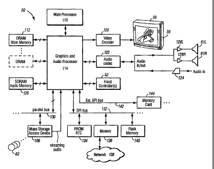
l0 Figure 2 shows a block diagram of example components of system 50.
The primary components include:
~ a main processor (CPU) 110,
~ a main memory 112, and
~ a graphics and audio processor 114.
In this example, main processor 110 (e.g., an enhanced IBM Power PC~
750) receives inputs from handheld controllers 52 (and/or other input devices)
via graphics and audio processor 114. Main processor 110 interactively
responds to user inputs, and executes a video game or other program supplied,
for example, by external storage media 62 via a mass storage access device 106
such as an optical disk drive. As one example, in the context of video game
play, main processor 110 can perform collision detection and animation
processing in addition to a variety of interactive and control functions.
In this example, main processor 110 generates 3D graphics and audio
commands and sends them to graphics and audio processor 114. The graphics
and audio processor 114 processes these commands to generate interesting
CA 02355794 2004-07-16
9
visual images on display 59 and interesting stereo sound on stereo
loudspeakers
61 R, 61 L or other suitable sound-generating devices.
Example system 50 includes a video encoder 120 that receives image
signals from graphics and audio processor 114 and converts the image signals
into analog and/or digital video signals suitable for display on a standard
display device such as a computer monitor or home color television set 56.
System 50 also includes an audio codec (compressor/decompressor) 122 that
compresses and decompresses digitized audio signals and may also convert
between digital and analog audio signaling formats as needed. Audio codec
l0 122 can receive audio inputs via a buffer 124 and provide them to graphics
and
audio processor 114 for processing (e.g., mixing with other audio signals the
processor generates and/or receives via a streaming audio output of mass
storage access device 106). Graphics and audio processor 114 in this example
can store audio related information in an audio memory 126 that is available
for
audio tasks. Graphics and audio processor 114 provides the resulting audio
output signals to audio codec 122 for decompression and conversion to analog
signals (e.g., via buffer amplifiers 128L, 128R) so they can be reproduced by
loudspeakers 61 L, 61 R.
Graphics and audio processor 114 has the ability to communicate with
various additional devices that may be present within system 50. For example,
a parallel digital bus 130 may be used to communicate with mass storage
access device 106 and/or other components. A serial peripheral bus 132 may
communicate with a variety of peripheral or other devices including, for
example:
~ a programmable read-only memory (PROM) and/or real time
clock (RTC) 134,
CA 02355794 2004-07-16
~ a modem 136 or other networking interface (which may in turn
connect system 50 to a telecommunications network 138 such as the
Internet or other digital network from/to which program instructions
and/or data can be downloaded or uploaded), and
5 ~ flash memory 140.
A further external serial bus 142 may be used to communicate with additional
expansion memory 144 (e.g., a memory card) or other devices. Connectors
may be used to connect various devices to busses 130, 132, 142.
l0 Exam 1~ a Grauhics And Audio Processor
Figure 3 is a block diagram of an example graphics and audio processor
114. Graphics and audio processor 114 in one example may be a single-chip
ASIC (application specific integrated circuit). In this example, graphics and
audio processor 114 includes:
~ a processor interface 150,
~ a memory interface/controller 152,
~ a 3D graphics processor 154,
~ an audio digital signal processor (DSP) 156,
~ an audio memory interface 158,
~ an audio interface and mixer 1300,
~ a peripheral controller 162, and
~ a display controller 164.
3D graphics processor 154 performs graphics processing tasks. Audio
digital signal processor 156 performs audio processing tasks. Display
controller 164 accesses image information from main memory 112 and
provides it to video encoder 120 for display on display device 56. Audio
CA 02355794 2004-07-16
11
interface and mixer 1300 interfaces with audio codec 122, and can also mix
audio from different sources (e.g., streaming audio from mass storage access
device 106, the output of audio DSP 156, and external audio input received via
audio codec 122). Processor interface 150 provides a data and control
interface
between main processor 110 and graphics and audio processor 114.
Memory interface 152 provides a data and control interface between
graphics and audio processor 114 and memory 112. In this example, main
processor 110 accesses main memory 112 via processor interface 150 and
memory interface 152 that are part of graphics and audio processor 114.
l0 Peripheral controller 162 provides a data and control interface between
graphics and audio processor 114 and the various peripherals mentioned above.
Audio memory interface 158 provides an interface with audio memory 126.
Exam 1e Gra hits Pi en line
Figure 4 shows a graphics processing system including a more detailed
view of an exemplary Figure 3 3D graphics processor 154. 3D graphics
processor 154 includes, among other things, a command processor 200 and a
3D graphics pipeline 180. Main processor 110 communicates streams of data
(e.g., graphics command streams and display lists) to command processor 200.
Main processor 110 has a two-level cache 115 to minimize memory latency,
and also has a write-gathering buffer 111 for uncached data streams targeted
for
the graphics and audio processor 114. The write-gathering buffer 111 collects
partial cache lines into full cache lines and sends the data out to the
graphics
and audio processor 114 one cache line at a time for maximum bus usage.
Command processor 200 receives display commands from main
processor 110 and parses them -- obtaining any additional data necessary to
CA 02355794 2004-07-16
12
process them from shared memory 112 via memory controller 152. The
command processor 200 provides a stream of vertex commands to graphics
pipeline 180 for 2D and/or 3D processing and rendering. Graphics pipeline
180 generates images based on these commands. The resulting image
information may be transferred to main memory 112 for access by display
controller/video interface unit 164 -- which displays the frame buffer output
of
pipeline 180 on display 56.
Figure 5 is a block logical flow diagram portraying illustrative
processing performed using graphics processor 154. Main processor 110 may
l0 store graphics command streams 210, display lists 212 and vertex arrays 214
in
main memory 112, and pass pointers to command processor 200 via bus
interface 150. The main processor 110 stores graphics commands in one or
more graphics first-in-first-out (FIFO) buffers 210 it allocates in main
memory
110. The command processor 200 fetches:
~ command streams from main memory 112 via an on-chip FIFO
memory buffer 216 that receives and buffers the graphics commands
for synchronization/flow control and load balancing,
~ display lists 212 from main memory 112 via an on-chip call FIFO
memory buffer 218, and
~ vertex attributes from the command stream and/or from vertex arrays
214 in main memory 112 via a vertex cache 220.
Command processor 200 performs command processing operations 200a
that convert attribute types to floating point format, and pass the resulting
complete vertex polygon data to graphics pipeline 180 for
rendering/rasterization. A programmable memory arbitration circuitry 130 (see
Figure 4) arbitrates access to shared main memory 112 between graphics
CA 02355794 2004-07-16
13
pipeline 180, command processor 200 and display controller/video interface
unit 164.
Figure 4 shows that graphics pipeline 180 may include:
~ a transform unit 300,
~ a setup/rasterizer 400,
~ a texture unit 500,
~ a texture environment unit 600, and
~ a pixel engine 700.
Transform unit 300 performs a variety of 2D and 3D transform and other
operations 300a (see Figure S). Transform unit 300 may include one or more
matrix memories 300b for storing matrices used in transformation processing
300a. Transform unit 300 transforms incoming geometry per vertex from
object space to screen space; and transforms incoming texture coordinates and
computes projective texture coordinates (300c). Transform unit 300 may also
perform polygon clipping/culling 300d. Lighting processing 300e also
performed by transform unit 300b provides per vertex lighting computations
for up to eight independent lights in one example embodiment. Transform unit
300 can also perform texture coordinate generation (300c) for embossed type
bump mapping effects, as well as polygon clipping/culling operations (300d).
2o Setup/rasterizer 400 includes a setup unit that receives vertex data from
transform unit 300 and sends triangle setup information to one or more
rasterizer units (400b) performing edge rasterization, texture coordinate
rasterization and color rasterization.
Texture unit 500 (which may include an on-chip texture memory
(TMEM) 502) performs various tasks related to texturing including for
example:
CA 02355794 2004-07-16
14
~ retrieving textures 504 from main memory 112,
~ texture processing (500a) including, for example, mufti-texture
handling, post-cache texture decompression, texture filtering,
embossing, shadows and lighting through the use of projective
textures, and BLIT with alpha transparency and depth,
~ bump map processing for computing texture coordinate displacements
for bump mapping, pseudo texture and texture tiling effects (SOOb),
and
~ indirect texture processing (SOOc, 500d).
to Texture unit 500 outputs filtered texture values to the texture
environment unit 600 for texture environment processing (600a). Texture
environment unit 600 blends polygon and texture color/alpha/depth, and can
also perform texture fog processing (600b) to achieve inverse range based fog
effects. Texture environment unit 600 can provide multiple stages to perform a
variety of other interesting environment-related functions based for example
on
color/alpha modulation, embossing, detail texturing, texture swapping,
clamping, and depth blending.
Pixel engine 700 performs depth (z) compare (700a) and pixel blending
(700b). In this example, pixel engine 700 stores data into an embedded (on-
chip) frame buffer memory 702. Graphics pipeline 180 may include one or
more embedded DRAM memories 702 to store frame buffer and/or texture
information locally. Z compares 700a' can also be performed at an earlier
stage
in the graphics pipeline 180 depending on the rendering mode currently in
effect (e.g., z compares can be performed earlier if alpha blending is not
required). The pixel engine 700 includes a copy operation 700c that
periodically writes on-chip frame buffer 702 to memory portion 113 of main
CA 02355794 2004-07-16
memory 112 for access by display/video interface unit 164. This copy
operation 700c can also be used to copy embedded frame buffer 702 contents to
textures in the main memory 112 for dynamic texture synthesis effects. Anti-
aliasing and other filtering can be performed during the copy-out operation.
5 The frame buffer output of graphics pipeline 180 (which is ultimately stored
in
main memory 112) is read each frame by display/video interface unit 164.
Display controller/video interface 164 provides digital RGB pixel values for
display on display 56.
l0 Examine Audio So s
Audio DSP 156 performs pitch modulation and the mixing of voices and
effects data. Audio DSP 156 is augmented by a large quantity (e.g., 16 MB or
more) of audio memory 126 (auxiliary RAM--ARAM) that may be used to
store audio samples. Audio is routed to speakers 61 L and 61 R via audio codec
15 122 which includes a digital-to-analog converter. Streaming audio from mass
storage device 62 provides an efficient method for reproducing high-fidelity
audio during game runtime.
Figure 6 is a more detailed block diagram of audio DSP 156, audio
memory interface 158 and audio interface and mixer 160 shown in Figure 3. A
sample rate converter 801 samples streaming audio (which may be from mass
storage device 62) at either 48 kHz or 32 kHz and L/R volume control 803
controls the left- and right-channel volume levels of the sampled audio. The
streaming audio bypasses main memory 112 entirely, thereby conserving
memory and processor bandwidth. In cases in which audio data on mass
storage device 62 is encoded, for example, in ADPCM format, mass storage
CA 02355794 2004-07-16
16
access device 106 automatically decodes the ADPCM data into PCM samples
(e.g., 16 bits) for supply to sample rate converter 801.
A DMA channel 805 enables the transfer of data from an arbitrary
location in main memory 112 to FIFO buffer 807. Mixer 809 mixes the outputs
of sample rate converter 801 and FIFO buffer 807 and the result is output to
audio codec 122. The sampling rate of audio codec 122 is, for example, 48
kHz and audio codec 122 may be a standard SigmaDelta codec for converting
stereo, 16-bit PCM into an analog signal.
DSP core 811 has a 100 MHz instruction clock and uses 16-bit data
to words and addressing. DSP core 811 uses a word (16-bit) addressable
instruction memory 813 that includes a RAM area (e.g., 8 kbyte) and a ROM
area (e.g., 8 kbyte) and a word addressable data memory 815 that includes a
RAM area (e.g., 8 kbyte) and a ROM area (e.g., 4 kbyte). A DSP DMA 819 is
provided to transfer data from/to main memory 112 to/from the DSP
data/instruction RAM areas, or from the DSP data/instruction ROM areas to
main memory 112. There are two requestors of access to instruction memory
813: DSP DMA 819 and DSP 811. The instruction RAM area can be
read/write by DSP DMA 819 and can be read only by DSP 811. The
instruction ROM area can only be read by DSP 811. There are three requestors
of access to data memory 815: DSP DMA 819, data bus 1 and data bus 2. Mail
box registers 817 are provided for communication with the main processor 110.
Mail box registers 817 may include a first mail box register for
communications from main processor 110 to DSP core 811 and a second mail
box register for communications from DSP core 811 to main processor 110.
Each register is, for example, 32-bits wide. An accelerator 821 is usable
instead of DSP core 811 to read from and write to audio memory 126. A
CA 02355794 2004-07-16
17
memory controller 823 is provided for audio memory 126 and is operative,
among other things, to arbitrate requests for audio memory access between
DSP core 811 and a dedicated DMA channel 825 controlled by main processor
110 for data transactions between audio memory 126 and main memory 112.
Generally, data transactions between audio memory 126 and DSP data memory
815 have priority over DMA channel 825. A decoder 827 decodes audio
samples supplied thereto. Audio memory 126 is intended primarily for the
storage of audio-related data and may comprise 16 MB of SDRAM
(expandable up to a total of 48 MB).
To help reduce audio data storage requirements, various compression and
decompression schemes may be utilized. ADCPM refers to adaptive
differential PCM. This scheme may be used to compress/decompress sounds
generated by the audio subsystem described above and to compress/decompress
sounds on mass storage device 62. Various ADPCM algorithms exist and it is
not necessary that the same algorithm be used for the sounds generated by the
audio subsystem and the sounds on mass storage device 62. Decoder 827
provides runtime ADPCM decompression of sound data generated by the audio
subsystem, and mass storage access device 106 provides runtime ADPCM
decompression of sound data from mass storage device 62. An 8-bit PCM
compression/decompression scheme may also be used for sound data generated
by the audio subsystem. Thus, decoder 827 also provides runtime
decompression of 8-bit PCM-compressed sound data. Of course, the
mentioned compression/decompression schemes are provided by way of
illustration, not limitation.
During system initialization, a runtime audio library is downloaded to
audio DSP 156. This audio library is used by audio DSP 156 to process and
CA 02355794 2004-07-16
18
mix voices in accordance with commands in a command list generated by main
processor 110. The command list is stored in main memory 112. Audio DSP
156 retrieves the commands from main memory and executes them in
accordance with the runtime audio library downloaded thereto. Figures 7A and
7B illustrate data flow and control flow, respectively, for reproducing
sounds.
As shown in Figure 7A, sound samples are read from mass storage device 62
into main memory 112 via peripheral (I/O) controller 162 and from main
memory 112 into audio memory 126 via ARAM DMA 825. The sound
samples are read by DSP core 811 via accelerator 821 and DSP core 811
l0 processes/mixes the sound samples. The processed/mixed sound samples are
buffered in main memory 112 and then transferred to audio interface FIFO 807
for output to speakers 61 L, 61 R via audio codec 122. As shown in Figure 7B,
the game application ultimately dictates the need for sound. The game
application makes a call to the audio system (main processor) runtime
application which generates a command list for audio DSP 156. In executing
the command list, audio DSP 156 retrieves the appropriate sound sample and
processes it as needed.
The data and control flow for music synthesis is similar to that for sound
samples shown in Figure 7A. The instrument wavetable from mass storage
device 62 is stored in audio memory 126 via main memory 112. Audio DSP
156, upon receiving commands generated by the audio system (main processor)
run time application, retrieves the necessary instrument samples, processes
and
mixes them, and stores the result in main memory 112. From there, the result
is
transferred to audio interface FIFO 807 for output to speakers 61 L, 61 R via
audio codec 122. The commands generated by the audio system (main
processor) run time application are driven by the music score which is read
CA 02355794 2004-07-16
19
from mass storage device 62 into main memory 112 and which is processed and
sequenced by the audio system (main processor) run time application according
to the demands of the game.
The audio system (main processor) run time application may also
manage the playback and mixing of audio tracks to provide software streaming.
Software streaming allows the simultaneous playback of one or more audio
tracks, which provides a degree of interactivity. The game may, for example,
fade from one track into another to influence the player's mood. In general,
the
different audio tracks are buffered in audio memory 126 as individual sound
l0 samples. Audio DSP 156 may then retrieve the tracks and mix them just as it
would any other voice.
The audio system permits placing of sound emitters in three-dimensional
space. This is achieved with the following features:
~ Volume and panning control
~ Pitch modulation (for Doppler effect)
~ Initial time delay (phase shift between left and right channels)
~ FIR filter (for HRTF and environmental effects)
Together these features provide a powerful means of generating psycho-
acoustic three-dimensional sound effects with a pair of speakers.
The voice processing pipeline is shown in Figure 8:
1. Samples are read from audio memory 126 by audio DSP 156.
2. ADPCM and 8-bit PCM samples from audio memory 126 are
decoded and the decoded samples are supplied to a first sample rate converter.
3. 16-bit PCM samples from audio memory 126 are passed directly
to the first sample rate converter.
CA 02355794 2004-07-16
4. The sample rate converter adjusts the pitch of the incoming
samples.
5. An FIR filter applies an optional, user-defined filter to the
samples.
5 6. A volume ramp applies a volume ramp across samples for volume
envelope articulation.
7. A mixer mixes the samples at a 32 kHz sampling rate with 24-bit
precision.
Steps 1-7 are repeated for each voice. When all of the voices have been
1o processed and accumulated in the mixer buffer, the following steps occur:
1. Dolby surround and main processor-based effects (such as reverb
or chorus) are applied to the mixed voices.
2. The samples are truncated from 24-bit to 16-bit precision, the data
is converted to a 48 kHz sample rate for output by the audio codec 122, and
the
15 result is output to main memory 112.
Figure 9 is a detailed block diagram of audio memory controller 823.
Audio memory controller 823 performs the following functions:
~ After reset, provides audio memory initial timing generation to stabilize
audio memory (includes audio memory mode setting);
20 ~ Generates audio memory refresh cycles; and
~ Accepts read/write requests of DMA 825 and accelerator 821 and then
generates access timing to audio memory 126.
A timing generation circuit 928 generates the access timing. In the
example system, there are up to two memory devices that make up audio
memory 126. The first is internal audio memory 926a and has a maximum size
of 8 Mbyte. The second is expansion audio memory 926b and has a maximum
CA 02355794 2004-07-16
21
size of 32 Mbyte. The addresses of internal audio memory 926a start from 0,
and the addresses of expansion audio memory 926b are cascaded onto the
ending address of the internal audio memory. Thus, the address spaces of
internal audio memory 926a and expansion audio memory 926b are
consecutive and the starting address of expansion audio memory 926b depends
on the size of internal audio memory 926a. The mode setting and refresh
cycles of internal audio memory 926a and expansion audio memory 926b are
active simultaneously.
After a reset, audio memory controller 823 initializes audio memory 126
(as represented by "ARAM initialization" 934 in Figure 9). During
initialization, controller 823 masks any access to audio memory 126; after
initialization, audio memory 126 is freely accessible. A flag ARAM NORM
may be set as an indication that initialization has been performed. As
mentioned above, the initialization includes audio memory mode setting. The
following settings may be set in an audio memory mode register:
~ Burst length (e.g., 2 bytes),
~ Addressing mode (e.g., sequential),
~ CAS latency (2 or 3 - programmed by main processor 110), and
~ Write mode (burst read and burst write).
Audio memory controller 823 initializes internal audio memory 926a and
expansion audio memory 926b simultaneously. Main processor 110 programs
CAS latency before initialization is finished. If CAS latency is not
programmed by main processor 110, the reset default CAS = 3 is used to access
audio memory 126.
After initialization, audio memory controller 823 determines the sizes of
internal audio memory 926a and expansion audio memory 926b.
CA 02355794 2004-07-16
22
Except for a chip select signal, internal audio memory 926a and
expansion audio memory 926b share the same address bus, data bus and control
signals. During operation, an arbitration unit 930 generates access timing for
three requesters:
~ DMA 825,
~ Accelerator 821, and
~ Refresh counter 932.
The priority among these requesters is as follows:
Refresh counter 932 > accelerator 821 > DMA 825
to The auto refresh period is programmable and audio memory controller
823 provides refresh cycles to internal audio memory 926a and expansion
audio memory 926b at the same time.
The following DSP-programmed bit can be used to mask access to audio
memory 126 by DMA 825:
AMDM:Ara M-Dma request Mask DSPaddress: OxFFEF
Bits Name Type Reset Description
15...1 R 0x0 Reserved
0 DMA request mask R/W 0x0 0: DMA request ARAM is unmasked
1: DMA request ARAM is masked
If bit 0 of AMDM is set, access to audio memory 126 is dedicated to
accelerator 821. If bit 0 of AMDM is clear, the following process occurs.
Typically, DMA 825 accesses audio memory 126 via a plurality (e.g.,
16) of read/write commands. If accelerator 821 needs to access audio memory
126 during this time, audio memory controller 823 determines whether both are
attempting to access the same bank of audio memory 126. If so, audio memory
CA 02355794 2004-07-16
23
controller 823 terminates (precharges) access by DMA 825 and transfers access
to accelerator 821. After accelerator 821 finishes, audio memory controller
823
transfers access back to DMA 825 and DMA 825 executes (activate first) the
rest of its read/write commands.
s If accelerator 821 and DMA 825 are accessing different banks, an
interleaved bank access scheme is utilized to realize better performance on
access transfer between accelerator 821 and DMA 825. In this scheme, audio
memory controller 823 does not precharge (terminate) the DMA bank, leaving
it on waiting. Access to audio memory 126 is then transferred to accelerator
l0 821. After accelerator 821 finishes its access of audio memory 126, audio
memory controller 823 executes (no need to activate first) the rest of the
read/write commands of DMA 825.
If access of audio memory 126 crosses a 512 byte boundary (different
row), audio memory controller 823 precharges the current row to end access
15 and activates the next row to start access. This increases the number of
cycles
to read/write data. The interleaved bank scheme described above is preferably
not provided for DMA-access-cross-row or accelerator-access-cross-row.
The details of the audio memory DMA 825 are shown in Figure 1 OA.
Audio memory DMA 825 includes an ARAM controller interface 952, and
2o three registers 900a-900c that are used to define main memory starting
address,
audio memory starting address, and the block length and the direction of the
DMA transfer, respectively. Main processor 110 programs these registers. The
registers are 32-bits wide and the DMA transfer direction is specified by bit
15
of the high word of the block length register. The starting address of each
side
25 (i.e., main memory 112, audio memory 126) is located at 32 byte boundary
and
the block length is a multiple of 32 bytes. During DMA transfer, these
registers
CA 02355794 2004-07-16
24
are modified by each memory controller block access. There is a one memory
controller size (32 byte) data buffer 950 built into the audio memory DMA to
bridge the unequal bandwidth memories.
The operation flow of main memory 110 to audio memory 126 includes
the following steps:
1. A write to the low word of block length register 900c triggers
DMA 825 as ready to transfer data.
2. DMA 825 sends a read request to memory controller 152 (Figure
3) and then waits for 32 byte data coming to DMA data buffer 950.
l0 3. Once the 32 byte data is moved into data buffer 950, DMA 825
sends a write request to arbitration circuit 930 (see Figure 9) and waits for
transfer. Main memory address register 900a is also increased by 32 by address
incrementing circuit 960.
4. If DMA 825 is granted access to audio memory 126 by arbitration
circuit 930, a write command is sent to audio memory 126 and data starts to
move from DMA data buffer 950 to audio memory 126 byte by byte, until 32
bytes have been moved (buffer empty). The audio memory address is increased
by 32 by audio address incrementing circuit 962 and the block length is
decreased by 32 by block length decrementing circuit 964.
5. Steps 2 through 4 are repeated until the block length reaches 0. At
this point, DMA 825 stops and control logic 954 sets up a flag and generates
an
interrupt to main processor 110. The interrupt is maskable.
The operation flow of audio memory 126 to main memory 110 includes
the following steps:
1. A write to the low word of block length register triggers DMA 825
ready to transfer data.
CA 02355794 2004-07-16
2. DMA 825 sends a read request to arbitration circuit 930 (see
Figure 9) and then waits for 32 byte data.
3. If DMA 825 is granted access to audio memory 126 by arbitration
circuit 930, a read command is sent to audio memory 126 and data starts to
5 move from audio memory 126 to DMA data buffer 950 byte by byte until 32
bytes have been moved into the data buffer. The audio memory address in
audio memory address register 900b is then increased by 32 by audio address
incrementing circuit 962.
4. Once 32 byte data is moved into DMA data buffer 950, DMA 825
10 sends a write request to memory controller 152. The 32 byte data is then
moved from DMA data buffer 950 to the memory controller bus. After this, the
address of main memory 110 is increased by 32 by main memory address
incrementing circuit 960 and the block length is decreased by 32 by clock
length decrementing circuit 964.
15 5. Steps 2 through 4 are repeated till the block length reaches 0. At
this point, DMA 825 stops and control logic 954 sets up a flag and generates
an
interrupt to main processor 110. The interrupt is maskable.
Arbitration is performed before each 32 byte transfer. The memory
controller bus arbitration priority is as follows:
2o AI DMA 805 > DSP DMA 819 > ARAM DMA 825
Figure l OB is a block diagram illustrating the details of DSP DMA 819.
As mentioned above, DSP DMA 819 functions to transfer data from/to main
memory 112 to/from the DSP data/instruction RAM areas or from the DSP
data/instruction ROM areas to main memory 112. DSP DMA 819 includes
25 three registers 796a-796c that are used to define a block length, a main
memory
address and a DSP memory address. A 2 x 32 byte FIFO 792 is used for the
CA 02355794 2004-07-16
26
data transfer and a 64-bit data bus provides high speed data transfer between
FIFO 792 and audio memory 126. The main memory starting address is
located at a 4 byte boundary and the DSP starting address is located at a 2
word
(32 bit) boundary. The block length is a multiple of 4 bytes. A control
register
of DSP DMA 819 includes a first bit that specifies the DMA transfer direction
and a second bit that specifies whether the data memory or the instruction
memory is involved in the DMA transfer. The control register also includes a
DSP DMA busy bit for providing DSP DMA status via control logic 790. The
busy bit is set once the DSP DMA is enabled and is cleared when the block
length in the block length register equals 0.
DSP DMA 819 is enabled by DSP 811 writing to block length register
796a. Once DSP DMA 819 is enabled, it requests that memory controller 152
grant access to main memory. When access is granted, data transfer is started.
As the data transfers continues, address changing circuits 798 and 799
increase
the access address of main memory 112 and DSP memory in registers 796b and
796c, respectively. The block length in register 796a is decreased in
accordance with block length changing circuit 797 as the blocks are
transferred.
The transfer continues until the block length register is 0 and the DMA
operation is then stopped. Data alignment and DSP memory control is effected
2o by control circuit 794.
When data is transferred from main memory 112 to DSP memory, if
FIFO 792 is full, DSP DMA 819 will wait for FIFO not full and then refill from
main memory 112 again. If FIFO 792 is not empty, DMA will transfer data of
FIFO to DSP memory until FIFO is empty. When data is transferred from DSP
memory to main memory 112, if FIFO 792 is empty, DSP DMA 819 will wait
CA 02355794 2004-07-16
27
for FIFO not empty and then transfer data of FIFO to main memory 112. If
FIFO is not full, DMA will refill FIFO from DSP memory until FIFO is full.
Example DSP DMA relative registers are:
DSMAH: DSp dma Main memory Address High DSPaddress OxFFCE
Bits Name Type Reset Description
15..10 6 bits R 0x0 This register is used to specify
of its DSP
MSBs DMA main memory starting/current
address from bit 31 to bit 26,
and
always 0
9..0 Main R/W undefinedThis register is used to specify
DSP
memory DMA main memory starting/current
address address from bit 25 to bit 16
high word
DSMAL: DSp dma Main memory Address Low DSPaddress OxFFCF
Bits Name Type Reset Description
15..2 Main R/W undefinedThis register is used to specify
DSP
memory DMA main memory starting/current
address address from bit 15 to bit 2
1,0 2 bits R 0x0 The main memory address of this
of its
LSBs DMA should be located at 4 byte
boundary
DSPA: DSp dma dsP memory Address High DSPaddress OxFFCD
Bits Name Type Reset Description
15..1 DSP R/W undefined This register is used to specify
DSP
CA 02355794 2004-07-16
28
memory memory starting/current address
from
address bit 15 to bit 1
0 1 bit of R 0x0 The DSP memory address should
its be
LSBs located at 2 word boundary
DSBL: DSp dma Block Length DSPaddress OxFFCB
Bits Name Type Reset Description
15..2 block R/W 0x0 This register is used to specify
DSP
length DMA transfer length from bit 15
to bit
2
1,0 2 bit of R 0x0 The transfer length is a multiple
its of 4
LSBs bytes
DSCR: DSp dma Control Register DSPaddress OxFFC9
Bits Name Type Reset Description
15..3 R 0x0 reserved
2 DSP DMA R 0x0 Block length counter not yet zero,
busy DMA is still busy
1 DSP R/W 0x0 DMA involved DSP memory
source/ 0: DSP data memory
destination 1: DSP instruction memory
0 transfer R/W 0x0 0: from main memory to DSP memory
direction 1: from DSP memory to main memory
In the example system, the instruction RAM is made of four copies of
256 x 64-bit synchronous one way dual port SRAM and the instruction ROM is
CA 02355794 2004-07-16
29
made of two copies of 2048 x 16-bit synchronous single port ROM. The
instruction RAM and the instruction ROM are independent of each other, so
while a read/write DMA operation is carried out for the instruction RAM, DSP
core 811 can access the instruction ROM. In addition, while DSP DMA 819
writes to the instruction RAM, DSP core 811 can read the instruction RAM. To
avoid hardware conflicts, the write and read addresses for the simultaneous
read/write should be different.
The data RAM is organized as 4 pages, each page being 1 kword in size.
The data ROM is organized as 1 page having a size of 2 kword. One data RAM
l0 page is made up of four copies of 256 x 16-bit synchronous one way dual
port
SRAM and the data ROM page is made up of a copy of 2048 x 16-bit
synchronous single port ROM. Each page is independent of the other pages so
that each page has its own data, address busses and read, write control
signals
to connect to the three requestors. Data in/out ports for DSP buses 1 and 2
are
16 bits wide and the data in/out ports for DSP DMA 819 are 64 bits. In this
arrangement, up to three pages can be active simultaneously for three
requestors.
In this example system, each SRAM page can be accessed by one read or
one write or one read and one write, but cannot be accessed by two reads or
two
2o writes. The reads could be DSP bus 1 or 2 or DSP DMA read and the writes
could be DSP bus 1 or 2 or DSP DMA write. The ROM page can only be
accessed by one read and the read can be a DSP bus 1 or 2 read. DSP DMA
819 cannot read the data ROM. If a page is being read by DSP DMA, DSP 811
can still write the page or read/write other pages. If a page is being written
by
DSP DMA 819, DSP 811 can still read the page or read/write other pages. To
avoid hardware conflicts, the DSP read and the DMA write or the DSP write
CA 02355794 2004-07-16
and DMA read should not occur on the same address location. DSP 811 is not
allowed to read the page that the DMA is reading and the DSP is not allowed to
write the page to which the DMA is writing.
Figure lOC is a block diagram of accelerator 821. As mentioned above,
5 accelerator 821 is used instead of DSP core 811 to read from and write to
audio
memory 126. Accelerator 821 includes a following addresses generating
circuit 902 for automatically increasing the address or generating a wrap
around address (circular addressing) for the next access. Accelerator 821
includes three data lines 904a-904c that function as pre-fetch buffers during
1 o read operations and as write buffers during write operations. As will be
explained below, data lines 904a-904c hide the access latency of audio memory
126 when operations of DSP core 811 access audio memory 126. An interrupt
to DSP core 811 is generated when data of the starting address is read by the
DSP or when data of the ending address is written to the data lines by the
DSP.
15 Three parameter registers (current address, starting address, ending
address) 906a-906c are used to define a circular buffer in the memory space of
audio memory 126. Each parameter register is 27 bits wide and can be
read/write by the audio DSP. Following addresses generation circuit 902 adds
"1" to the current address to obtain the next address. If the current address
is
20 equal to the ending address, then the next address is the starting address.
Parameter registers 906a-906c are used for reading from and writing to audio
memory 126. The relationship between the addresses and the data in the
registers is as follows:
ACCAH: Accelerator aram Current Address High DSP Address:OxFFD8
Bits Name Type Reset Description
15 Direction R/W 0x0 O:accelerator read ARAM
CA 02355794 2004-07-16
31
l :accelerator write ARAM
14...11 R 0x0 Reserved
10...0 Current address R/W 0x0 Bit 26 to bit 16 of ARAM
high-word current address
ACCAL: Accelerator aram Current Address Low DSP Address:OxFFD9
Bits Name Type Reset Description
15...0 Current address R/W 0x0 Bit 15 to Bit 0 of ARAM
low-word current address
ACEAH: Accelerator aram Ending Address High DSP Address:OxFFD6
Bits Name Type Reset Description
15...11 R 0x0 Reserved
10...0 Ending address R/W 0x0 Bit 26 to bit 16 of ARAM
high-word ending address
ACEAL: Accelerator aram Ending Address Low DSP Address:OxFFD7
Bits Name Type Reset Description
15...0 Ending address R/W 0x0 Bit 15 to bit 0 of ARAM
low-word ending address
ACSAH: Accelerator aram Starting Address High DSP Address:OxFFD4
Bits Name Type Reset Description
15...11 R 0x0 Reserved
10...0 Starting address R/W 0x0 Bit 26 to bit 16 of ARAM
CA 02355794 2004-07-16
32
high-word starting address
ACSAL: Accelerator cram Starting Address Low DSP Address:OxFFDS
Bits Name Type Reset Description
15...0 Starting addressR/W 0x0 Bit 15 to bit 0 of ARAM
low-word starting address
Data lines 904a-904c are each 16 bits in width. For read operations, the
data lines function as pre-fetch data buffers in which data is read from audio
memory 126 in advance and is ready to deliver as DSP core 811 reads the data
lines. For write operations, the data lines functions are temporary buffers
for
the data from DSP core 811 that is to be written to audio memory 126. Data
lines 904a-906c are formed in a FIFO manner, the in/out port thereof being
1o readable/writeable by DSP core 811. The addresses of the data in the data
lines
correspond to the current address and its two following addresses.
The audio subsystem described herein enables sound emitters to be
placed in three-dimensional space and provides a powerful means of generating
psycho-acoustic 3D sound effects with a pair of speakers. The audio subsystem
includes an audio memory that is usable, for example, to store sound samples,
instrument wave tables, audio tracks and the like read from a mass storage
device such as a DVD. The samples, wave tables, tracks, etc. are subsequently
read out and processed by an audio digital signal processor to produce the
game
audio content. This content is transferred to a main memory from where it is
2o subsequently read out for supply to a decoder and output to speakers. The
separate audio memory improves the access for the audio processing circuitry
CA 02355794 2004-07-16
33
to audio data by avoiding the need to contend with other resources (e.g., the
graphics subsystem) attempting to access the main system memory.
The provision of an audio memory 126 as described herein provides an
opportunity to further enhance the system's ability to efficiently provide
access
to data to those resources that need such access. For example, a DVD has a
relatively high "latency", i.e., it takes a relatively long time for data to
be
returned responsive to a request for the data. Therefore, it is useful to pre-
fetch
data such as animation data and compressed graphics data from the DVD prior
to the time that the data is needed so that the data can be quickly provided
to a
l0 component needing the data. The audio memory may be used as a cache for
this "pre-fetched" non-audio-related data. Then, when the non-audio-related
data is needed, for example in the rendering pipeline, DMA circuit 825 is used
to transfer the data to main memory 112 where it becomes available to the
component that needs it. The data transferred to the main memory may be
decompressed, if appropriate.
In the example system, audio memory 126 does not have a direct
interface with mass storage device 62. Thus, the non-audio-related data for
pre-caching is read from mass storage device 62 via peripheral controller 162
to
main memory 112 and then written via ARAM DMA 825 to audio memory
2o 126. The non-audio-related data is then later read via ARAM DMA 825 back
to main memory 112 when needed, for example, in the rendering pipeline. Of
course, in other implementations, audio memory 126 may be provided with a
direct interface to mass storage device 62 and the non-audio-related data may
be "pre-cached" in audio memory 126 without first passing through main
memory 112.
CA 02355794 2004-07-16
34
The runtime audio library includes a resource management algorithm
that monitors resource usage of audio DSP 156 and dynamically limits voice
allocation accordingly. This prevents audio DSP 156 from becoming
overburdened, which may result in corrupted audio output. Preferably, the
resource management algorithm assumes worst-case memory access latencies
to further ensure smooth, continuous audio. For example, up to 64 voices may
be supported, depending on the mixing and processing requirement of each
voice.
l0 Other Example Compatible Imylementations
Certain of the above-described system components 50 could be
implemented as other than the home video game console configuration
described above. For example, one could run graphics application or other
software written for system 50 on a platform with a different configuration
that
emulates system 50 or is otherwise compatible with it. If the other platform
can
successfully emulate, simulate and/or provide some or all of the hardware and
software resources of system 50, then the other platform will be able to
successfully execute the software.
As one example, an emulator may provide a hardware and/or software
configuration (platform) that is different from the hardware and/or software
configuration (platform) of system 50. The emulator system might include
software and/or hardware components that emulate or simulate some or all of
hardware and/or software components of the system for which the application
software was written. For example, the emulator system could comprise a
general-purpose digital computer such as a personal computer, which executes
a software emulator program that simulates the hardware and/or firmware of
CA 02355794 2004-07-16
system 50. The DSP processing of the above-described audio system could be
emulated on a personal computer.
Some general purpose digital computers (e.g., IBM or Macintosh
personal computers and compatibles) are now equipped with 3D graphics cards
5 that provide 3D graphics pipelines compliant with DirectX or other standard
3D graphics command APIs. They may also be equipped with stereophonic
sound cards that provide high quality stereophonic sound based on a standard
set of sound commands. Such multimedia-hardware-equipped personal
computers running emulator software may have sufficient performance to
10 approximate the graphics and sound performance of system 50. Emulator
software controls the hardware resources on the personal computer platform to
simulate the processing, 3D graphics, sound, peripheral and other capabilities
of the home video game console platform for which the game programmer
wrote the game software.
15 Figure 11 A illustrates an example overall emulation process using a host
platform 1201, an emulator component 1303, and a game software executable
binary image provided on a storage medium 62. Host 1201 may be a general or
special purpose digital computing device such as, for example, a personal
computer, a video game console, or any other platform with sufficient
20 computing power. Emulator 1303 may be software and/or hardware that runs
on host platform 1201, and provides a real-time conversion of commands, data
and other information from storage medium 62 into a form that can be
processed by host 1201. For example, emulator 1303 fetches "source" binary-
image program instructions intended for execution by system 50 from storage
25 medium 62 and converts these program instructions to a target format that
can
be executed or otherwise processed by host 1201.
CA 02355794 2004-07-16
36
As one example, in the case where the software is written for execution
on a platform using an IBM PowerPC or other specific processor and the host
1201 is a personal computer using a different (e.g., Intel) processor,
emulator
1303 fetches one or a sequence of binary-image program instructions from
storage medium 62 and converts these program instructions to one or more
equivalent Intel binary-image program instructions. The emulator 1303 also
fetches and/or generates graphics commands and audio commands intended for
processing by the graphics and audio processor 114, and converts these
commands into a format or formats that can be processed by hardware and/or
l0 software graphics and audio processing resources available on host 1201. As
one example, emulator 1303 may convert these commands into commands that
can be processed by specific graphics and/or or sound hardware of the host
1201 (e.g., using standard DirectX, OpenGL and/or sound APIs).
An emulator 1303 used to provide some or all of the features of the video
game system described above may also be provided with a graphic user
interface (GUI) that simplifies or automates the selection of various options
and
screen modes for games run using the emulator. In one example, such an
emulator 1303 may further include enhanced functionality as compared with
the host platform for which the software was originally intended.
Figure 11 B illustrates an emulation host system 1201 suitable for use
with emulator 1303. System 1201 includes a processing unit 1203 and a
system memory 1205. A system bus 1207 couples various system components
including system memory 1205 to processing unit 1203. System bus 1207 may
be any of several types of bus structures including a memory bus or memory
controller, a peripheral bus, and a local bus using any of a variety of bus
architectures. System memory 1207 includes read only memory (ROM) 1252
CA 02355794 2004-07-16
37
and random access memory (RAM) 1254. A basic input/output system (BIOS)
1256, containing the basic routines that help to transfer information between
elements within personal computer system 1201, such as during start-up, is
stored in the ROM 1252. System 1201 further includes various drives and
s associated computer-readable media. A hard disk drive 1209 reads from and
writes to a (typically fixed) magnetic hard disk 1211. An additional (possible
optional) magnetic disk drive 1213 reads from and writes to a removable
"floppy" or other magnetic disk 1215. An optical disk drive 1217 reads from
and, in some configurations, writes to a removable optical disk 1219 such as a
1o CD ROM or other optical media. Hard disk drive 1209, magnetic disk drive
1213, and optical disk drive 1217 are connected to system bus 1207 by a hard
disk drive interface 1221, a floppy disk drive interface 1223, and an optical
drive interface 1225, respectively. The drives and their associated computer-
readable media provide nonvolatile storage of computer-readable instructions,
15 data structures, program modules, game programs and other data for personal
computer system 1201. In other configurations, other types of computer-
readable media that can store data that is accessible by a computer (e.g.,
magnetic cassettes, flash memory cards, digital video disks, Bernoulli
cartridges, random access memories (RAMs), read only memories (ROMs) and
20 the like) may also be used.
A number of program modules including emulator 1303 may be stored
on the hard disk 1211, removable magnetic disk 1215, optical disk 1219 and/or
the ROM 1252 and/or the RAM 1254 of system memory 1205. Such program
modules may include an operating system providing graphics and sound APIs,
25 one or more application programs, other program modules, program data and
game data. A user may enter commands and information into personal
CA 02355794 2004-07-16
38
computer system 1201 through input devices such as a keyboard 1227, pointing
device 1229, microphones, joysticks, game controllers, satellite dishes,
scanners, or the like. These and other input devices can be connected to
processing unit 1203 through a serial port interface 1231 that is coupled to
system bus 1207, but may be connected by other interfaces, such as a parallel
port, game port Fire wire bus or a universal serial bus (USB). A monitor 1233
or other type of display device is also connected to system bus 1207 via an
interface, such as a video adapter 1235.
System 1201 may also include a modem 1154 or other network interface
l0 means for establishing communications over a network 1152 such as the
Internet. Modem 1154, which may be internal or external, is connected to
system bus 123 via serial port interface 1231. A network interface 1156 may
also be provided for allowing system 1201 to communicate with a remote
computing device 1160 (e.g., another system 1201) via a local area network
1158 (or such communication may be via wide area network 1152 or other
communications path such as dial-up or other communications means). System
1201 will typically include other peripheral output devices, such as printers
and
other standard peripheral devices.
In one example, video adapter 1235 may include a 3D graphics pipeline
chip set providing fast 3D graphics rendering in response to 3D graphics
commands issued based on a standard 3D graphics application programmer
interface such as Microsoft's DirectX 7.0 or other version. A set of stereo
loudspeakers 1237 is also connected to system bus 1207 via a sound generating
interface such as a conventional "sound card" 1239 providing hardware and
embedded software support for generating high quality stereophonic sound
based on sound commands provided by bus 1207. These hardware capabilities
CA 02355794 2004-07-16
39
allow system 1201 to provide sufficient graphics and sound speed performance
to play software stored in storage medium 62.
While the invention has been described in connection with what is
presently considered to be the most practical and preferred embodiment, it is
to
be understood that the invention is not to be limited to the disclosed
embodiment, but on the contrary, is intended to cover various modifications
and equivalent arrangements included within the scope of the appended claims.