Note: Descriptions are shown in the official language in which they were submitted.
CA 02356242 2001-06-19
WO 00/38324 PCTIUS99/30205
PLL AND GAIN CONTROL FOR CLOCK RECOVERY
Technical Field of the Invention
The present invention relates generally to clock recovery and in particular
the present invention relates to phase lock loop, trnasconductance circuitry
and
gain control circuitry for recovering a clock from high data rate signals.
Background of the Invention
Clock and data recovery in high speed data communication systems
require receiver circuits which can adjust an internal oscillator to a
frequency and
phase of the communicated data. For a description of clock recovery, see C. R.
Hogge, "A Self Correcting Clock Recovery Circuit," IEEE, J. Lightwave
Technol. LT-3 1312 (1985). Hogge describes a receiver circuit which adjusts a
recovered clock signal to center the clock signal transitions in a center of
the
communicated data signal.
The receiver circuits typically require a phase lock loop circuit to acquire
the clock signal from the transmitted data. Phase lock loop circuits adjust an
internal oscillator to match a phase of an externally supplied reference
signal,
such as the received data signal. These phase lock loop circuits compare the
reference signal to the internal oscillator signal and provide an output which
is
used to adjust the oscillator. For example, a parallel digital phase lock loop
architecture is described in Fiedler et al., "A 1.0625 Gbps Transceiver with
2x-
Oversampling and Transmit Signal Pre-Emphasis," ISSCC 1997 Dig. Tech.
Papers, 238 (1997).
High speed data recovery in a communication system operating in excess
of 1 GHz requires high speed components, a speed which is difficult to achieve
in complementary metal oxide semiconductor (CMOS) fabrication. In
particular, current CMOS fabrication sizes of about 0.18 to 0.35 micron have
NMOS transistors with a frequency cutoff f of about 10 to 15 GHz. Thus,
processing a signal with a frequency of about 1.25 GHz pushes the transistors
to
their limitations. Further, gain control in a conventional receiver circuit
adjusts
the input signal prior to processing with a phase lock loop. Using CMOS
processing, accurately adjusting the gain of the high frequency input data is
not
CA 02356242 2007-06-08
74842-12
2
presently possible. The economics of IC fabrication create
a need for a solution to high speed clock recovery using
CMOS technology.
For the reasons stated above, and for other
reasons stated below which will become apparent to those
skilled in the art upon reading and understanding the
present specification, there is a need in the art for a CMOS
receiver circuit capable of recovering a clock signal and
data in a high speed data communication system. Further,
there is a need for a receiver which can adjust gain to
changes in the communication data voltage.
Summary of the Invention
The above mentioned problems with high speed data
communication receiver circuits and other problems are
addressed by embodiments of the present invention and will
be understood by reading and studying the following
specification.
According to one aspect of the present invention,
there is provided a high speed data receiver comprising
differential input connections for receiving differential
analog input voltage signals, a phase detector circuit
coupled to receive the differential analog input voltage
signals and provide a differential analog voltage output, an
oscillator for providing a second input signal to the phase
detector, the receiver further comprising: a
transconductance circuit coupled between the phase detector
circuit and the oscillator for converting the differential
analog voltage output into an analog output current the
transconductance circuit having an adjustable gain based
upon adjusting a voltage of a bias circuit; and an automatic
gain control circuit, comprising an envelope detector and a
CA 02356242 2007-06-08
74842-12
2a
transconductance control circuit, coupled to the
transconductance circuit for providing the control voltage
signal in response to an amplitude differential of the
differential analog input voltage signals.
According to another aspect of the present
invention, there is provided a method of operating a
receiver, the method comprising: receiving differential
input signals; generating an analog voltage representing a
phase difference between the input signals and a second
signal; converting the analog signal into an analog current
using a transconductor circuit; detecting upper and lower
peak voltages of the input signals using an envelope
detector circuit; and adjusting a gain of the transconductor
circuit in response to a differential magnitude between the
upper and lower peak voltages.
Brief Description of the Drawings
Figure 1 is a block diagram of a data
communication system;
Figure 2 is a diagram of a dual loop phase lock
loop circuit of one embodiment of the present invention;
Figure 3 is a diagram of a fine loop circuit;
Figure 4 is a schematic diagram of a
transconductance circuit;
Figure 5 is a diagram of a coarse loop circuit;
Figure 6A is a schematic diagram of an input stage
for a transconductor;
Figure 6B is a graph illustrating operation of the
input stage of Figure 6A;
CA 02356242 2007-06-08
74842-12
2b
Figure 7A is a block diagram of a dual
transconductance circuit;
Figure 7B is a graph illustrating operation of the
dual transconductance circuit of Figure 7A;
Figure 8 is one embodiment of a transconductance
circuit including an automatic gain control circuit;
Figure 9 is another embodiment of a
transconductance circuit including an automatic gain control
circuit;
Figure 10 illustrates a block diagram of an
envelope detector circuit;
Figure 11 illustrates one embodiment of a positive
peak detector circuit; and
Figure 12 illustrates one embodiment of a negative
peak detector circuit.
CA 02356242 2001-06-19
WO 00/38324 PCT/US99/30205
3
Detailed Description of the Invention
In the following detailed description of the preferred embodiments,
reference is made to the accompanying drawings which form a part hereof, and
in which is shown by way of illustration specific preferred embodiments in
which the inventions may be practiced. These embodiments are described in
sufficient detail to enable those skilled in the art to practice the
invention, and it
is to be understood that other embodiments may be utilized and that logical,
mechanical and electrical changes may be made without departing from the
spirit
and scope of the present inventions. The following detailed description is,
therefore, not to be taken in a limiting sense, and the scope of the present
invention is defined only by the appended claims.
The term "serial" is used here to define a receiver architecture for which
the clock recovery and the data recovery are accomplished at the full data
rate,
for example 1.25 Gb/s. The serial approach requires circuits to operate with a
1.25 GHz clock rate - a requirement that is very difficult to achieve with a
0.25
or 0.35 m CMOS integrated circuit fabrication process.
The term "parallel" is used here to define a receiver architecture where
the input data stream is sampled at a sampling rate of at least the full data
rate,
such as 1.25 Gb/s or greater, and the sampled data is processed in several
parallel
paths. Each path can then operate with a relaxed clock rate compared to the
serial approach.
Referring to Figure 1, a communication system 100 is described which
operates at high communication speeds. The system includes transmitter 102
and receiver 104 units. The data connections 106 between the transmitter and
the receiver units can operate at data rate speeds of about 1.25 Gb/s or
greater.
The data connections 106 do not include a clock line for synchronizing the
receiving units with the transmitting units, but can include complementary
data
lines. As such, the receiving units include detection circuitry 108 for
recovering
the clock signal from the received data. In one embodiment, the detection
circuitry includes a dual loop phase lock loop (PLL) circuit connected to
receive
the incoming data signals. The dual loop function allows frequency acquisition
with a coarse loop and precise phase control with a fine loop. The receiver,
in
one embodiment, includes a transconductance function with a small value, such
CA 02356242 2001-06-19
WO 00/38324 PCT/US99/30205
4
as about 10 S (microSiemens). Further, a variable gain function can be
provided in the phase lock loop circuit to allow for variable input signal
voltages.
Figures 2-9 illustrate different embodiments of phase lock loop circuits
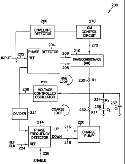
and transconductance circuitry. The basic phase lock loop circuit 200 includes
a
coarse loop, a fine loop, an envelope detector 260 and transconductance
control
circuitry 270 to control the value of the transconductance in the fine loop
(Figure
2). The transconductance control circuitry provides a control output on
connection 272, and embodiments of the envelope detector and transconductance
control circuitry are described in greater detail below. The fine loop uses a
phase
detector 204 which provides differential analog voltage outputs 206 and 208,
ViP
and ViN, respectively. The fine loop processes the input data provided on
complimentary data lines 202, as the phase reference for phase detector 204.
The analog outputs of the phase detector are converted to an analog current by
a
unique transconductance circuit 210. The analog output current is coupled to a
voltage controlled oscillator (VCO) 212. The VCO can be any kind of
oscillator,
including but not limited to a ring oscillator. The VCO is coupled to a second
input of the phase detector. In operation, the fine loop adjusts the VCO
signal to
correspond to the phase of the input data. In one embodiment, the voltage
controlled oscillator 212 is a five-stage ring oscillator which is tapped to
provide
ten output clock signals with the same frequency, but different phases.
The coarse PLL uses a reference clock signa1224, for example 62.5
MHZ, as a frequency reference for a phase-frequency detector (PFD) 214 for
rapid frequency acquisition. The PFD is coupled to a charge pump circuit 220
which in turn adjusts an input voltage of voltage controlled oscillator 212.
As
illustrated, VCO 212 is shared between the coarse and fine loops of the phase
lock loop circuit.
A detailed description of the phase lock loop circuitry is provided in the
following paragraphs. The phase lock loop circuit is broken into two halves,
the
fine and coarse loops. A description of the fine loop circuitry is first
provided,
followed by the coarse loop.
A schematic diagram of the fine PLL circuitry is given in Figure 3. The
phase detector (PD) 204 oversamples the input data by a factor of 2 and
provides
5 parallel data outputs at 1/5 the input data rate. Input data lines 202
comprise
CA 02356242 2001-06-19
WO 00/38324 PCTIUS99/30205
complementary data lines. The complementary data lines are referred to as a
negative data connection (dvn) 205 and a positive data connection (dvp) 207,
shown in Figures 9-12 below. The terms positive and negative define a relation
between the two connections, and do not represent a sign of the magnitude of
the
5 data signal provided thereon. Ten high-speed capture latches 250 are used to
convert the serial input data into parallel data paths. That is, the input
data is
sampled twice per data bit. One sample is in the middle of the data period and
the other sample is at the edge of the data period. The edge sample is used to
adjust the phase of the PLL circuit, and the middle sample is used as one of
the
five parallel data outputs.
The five middle samples are also used as a logic function to determine
the validity of the edge samples. When two adjacent middle samples have the
same value, then the intervening edge sample is invalid and is rejected. When
two adjacent middle samples differ in value, then the magnitude of the
intervening edge sample is valid and the sign of the value needs to be
determined. A positive sign is used for a positive transition, and a negative
sign
is used for a negative transition. When valid, the resulting edge sample is
proportional to the phase error.
When the input data is provided at 1.25 Gb/s, each path operates with a
0.250 GHz clock. The PD, therefore, produces a complementary pair of analog
voltage outputs 206 and 208 which have a differential voltage proportional to
the
phase error between the input data and a clock running at 5 times the voltage
controlled oscillator frequency.
The transconductance circuit 210 converts this differential analog voltage
to an analog current which passes through resistors 230 (R1) and 234 (R2) and
which changes the charge on capacitor 236. An optional capacitor 237 can be
coupled to resistor 234. The voltage divided by resistors 230 and 234 controls
the oscillator 212 input voltage. The effective one-sided transconductance of
the
transconductance circuit is about 10 S for a 1 V peak-to-peak single-ended
input signal. Thus, a 1-V, single-sided, peak-to-peak error voltage produces a
difference voltage of 2 V peak-to-peak and a 20 A peak-to-peak output current
( 10 A peak current centered around 0 A). The operation of the fine PLL can
be described by:
CA 02356242 2001-06-19
WO 00/38324 PCTIUS99/30205
6
K 4Sg"'TB (1)
1C C2
and
W
~ - 2 R2C2 (2)
where WN is the natural frequency and Cis the damping factor. In addition Ko
is
the VCO gain, S is the maximum slew rate of the input to the phase detector, g
is the one-sided transconductance of the transconductor circuit, TB is the bit
period, Rz is the filter resistance and Cz is the filter capacitance. Typical
values
of wN and Care 3.12 x 10'/s and 0.7, respectively. For these values, Ko = 2.43
x 109/s, S= 2V/ns, g,,, = 10 uS, TB = 0.8 ns, R2 = 900 ohms, and C2= 50 pF.
An important element in the receiver circuit 200 is the transconductance
circuit 210 which must convert a 1 V single-sided error voltage signal into a
current of approximately 10 A for controlling the voltage controlled
oscillator
212. In one embodiment, the transconductance circuit 210 also provides
variable
gain amplification, as described below. The transconductance circuit contains,
a
double-sided to single-sided converter, source degeneration resistors to
reduce
overall gain, and current mirrors to reduce the current at the output by a
factor of
A, also as explained below. In one embodiment, the reduction factor A is equal
to 10.
Figure 4, illustrates a schematic diagram of one embodiment of the
transconductance circuit. The transconductance circuit has an input stage 300
and an output stage 301. The input stage receives the differential voltage
outputs
from the phase detector circuit and provides intermediate outputs 350 and 351.
The input stage operates as a differential amplifier with active loads
(transistors
306 and 308) and degeneration resistors (310 and 312). In one embodiment,
degeneration resistors 310 and 312 are variable and controlled by the control
output signal on connection 272 from transconductance control circuit 270.
The input stage includes two n-channel input field effect transistors 302
and 304. A diode-connected (drain and gate connected) p-channel transistor 306
CA 02356242 2001-06-19
WO 00/38324 PCT/US99/30205
7
is connected between Vdd and the drain of transistor 302. Likewise, a p-
channel
transistor 308 is connected between Vdd and the drain of transistor 304. The
source of transistor 302 is coupled to Vss through resistor 310 and transistor
314,
and the source of transistor 304 is coupled to Vss through resistor 312 and
transistor 314. An optional capacitor 316 is provided between the sources of
transistors 302 and 304. In operation, variations in the differential input
voltages
on the gates of transistors 302 and 304 change currents through transistors
306
and 308. Thus, voltages on intermediate outputs 350 and 351 also change. The
intermediate outputs 350 and 351 are respectively coupled to p-channel
transistors 318 and 320, of the output stage 301. The currents through
transistors
306 and 308, therefore, are mirrored through transistors 320 and 318.
The output stage 301 provides a low current, high impedance output 360.
The output provides a current in response to the linear differential input
voltage.
The output stage includes a pull-up circuit and a pull-down circuit. The pull-
up
circuit includes transistors 318, 322, 324, 326, 328, 330, 332, 334 and 336.
Series connected n-channel transistors 322 and 324 are connected as diodes
(gate
coupled to drain) and conduct the same current mirrored in transistor 318.
Transistors 326 and 328 are sized to conduct one-tenth the current of
transistors
322 and 324, respectively. Thus, the current through transistors 322 and 324
is
mirrored and divided by ten through transistors 326 and 328. This reduced
current is mirrored through p-channel transistors 330 and 332 to p-channel
transistors 334 and 336. Transistors 334 and 336 are coupled to output node
360
to pull-up the output node and increase the output current.
The output stage pull-down circuit includes transistors 320, 340, 342,
344, and 346. Series connected n-channel transistors 340 and 342 are connected
as diodes (gate coupled to drain) and conduct the same current mirrored in
transistor 320. Transistors 344 and 346 are sized to conduct one-tenth the
current of transistors 340 and 342, respectively. Thus, the current through
transistors 340 and 342 is mirrored and divided by ten through transistors 344
and 346. Transistors 344 and 346 are coupled to output node 360 to pull-down
the output node and decrease the output current.
In operation, transistor 314 is activated and the differential voltage across
the gates of transistors 302 and 304 results in a current output at node 360.
Thus,
CA 02356242 2001-06-19
WO 00/38324 PCTIUS99/30205
8
as a voltage on the gate of transistor 302 increases, the current through
transistors 334 and 336 increases. Likewise, as a voltage on the gate of
transistor
304 increases, the current through transistors 344 and 346 increases.
A schematic diagram of the coarse loop is shown in Figure 5. The coarse
loop includes a phase frequency detector 214 which uses a reference clock (REF
CLK) input 224 and a divided down output of the VCO circuit 212. The output
of the VCO circuit is divided by four using divider circuit 222. An enable
signal
can be provided at inpui 226 to the phase frequency detector to inhibit the
operation of the coarse loop after frequency acquisition by the VCO. The phase
frequency detector provides output signals 216 and 218 to control charge pump
220. The charge pump provides an output current through resistor 232 (R, *).
Again, this current is coupled to resistor 234, capacitor 236 and the shared
oscillator circuit 212. Thus, the coarse loop is used to adjust the frequency
of the
VCO circuit to the reference clock (REF CLK) 224.
The coarse PLL can be described by:
tv* = K IP (3)
N 2 ~~
and
2 R1C? (4)
where W,* is the natural frequency and ~* is the damping factor. The asterisk
is
used here to identify variables associated with the coarse PLL. The variables
K ,
R*, RZ and CZ are similar to those defined for the fine PLL. Ip is the maximum
current of the charge pump 220 and N is equal to 4, which corresponds to the
divider (Divide by 4) circuit 222. Since both the transconductance 210 and
charge pump 220 circuits provide current pulses, resistors R, and R,* can be
made small. For example, the resistances can be 10052, or smaller, even zero.
The above described receiver embodiment provides a high speed clock
recovery circuit which operates on a I V single-sided peak-to-peak input
signal.
CA 02356242 2001-06-19
WO 00/38324 PCT/US99/30205
9
Because the input voltage can vary from 200 mV to 1 V single-sided peak-to-
peak, another embodiment of the receiver circuit includes variable gain
amplification to increase the one-sided transconductance from about 10 S to
about 50 S. Before describing a receiver circuit which includes variable gain
amplification, it is noted that the high speed data rates and a 0.25 to 0.35
Etm
CMOS fabrication process does not allow for reliable variable gain
amplification
at the input of the phase detector 204. Thus, the following embodiments
implement a unique variable gain amplifier implemented with the
transconductance circuit. It will be understood that in the above described
circuitry, the number of latches, data outputs, VCO stages, crystal frequency,
magnitude of the transconductance and the divider circuit is not critical to
the
invention. These numbers can be varied by one skilled in the art, upon reading
the present description, without deviating from the present invention.
As described above, the transconductance circuit 210 of Figures 3 and 4
includes an input stage 300 which is configured as a differential amplifier
with
active/transistor loads (306 and 308) and degeneration resistors (310 and
312).
In one embodiment of the transconductance circuit for the Gigabit receiver, a
transconductance of about 10 S is needed for a 1 V, single-sided, peak-to-
peak
voltage. The transconductance should increase to 50 S when a 200 mV, single-
sided peak-to-peak voltage is applied as input to the phase detector 204. A
transconductance circuit with an inverse linear relationship between the input
voltage magnitude and the transconductance is desired.
To illustrate a problem with achieving an inverse linear relationship, an
example input stage 450 is shown in Figures 6A and 6B. The g,,, value of this
circuit can be programmed by varying the value of the bias currents I. The
linear
range for the circuit of Figures 6A and 6B is defined as the region (V;+- V; )
where the slope of current I vs (V;+- V;") curve is constant to within a
predefined
linear specification. This slope is the g,,, value:
f
gm . - (5)
v, - v,
CA 02356242 2001-06-19
WO 00/38324 PCT/US99/30205
The linear range of the circuit of Figure 6A is directly proportional to the
excess bias voltage of transistors 452 and 454 (vdsat), and vdsat z Vgs -Vt.
Where Vgs is the gate to source voltage of transistors 452 and 454, and Vt is
the
threshold voltage of transistors 452 and 454. The following proportionality
5 relationships hold between the different parameters for circuit 450: linear
range
gn, vdsat I. Thus, as the g,,, value increases, the linear range for
circuit 450
increases. Likewise, as the g,,, value decreases, the linear range for circuit
450
decreases. This behavior is opposite of what is needed for the fine loop
transconductance circuit.
10 Figures 7A and 7B illustrate a transconductance circuit 500 which has an
inverse linear relationship between the input differential voltage and the
transconductance. The circuit 500 solves the problem of the relationship
between the gm value and the linear range, but also allows for a large
programming range. For a 3V CMOS process, circuit 500 can achieve a
programming range of 5X to l OX. Thus, the receiver could support input
voltages from 200mV to IV peak-to-peak single-ended. Transconductance
circuit 500 can be used as one embodiment of transconductance circuit 210 of
Figure 2.
The circuit of Figure 7A has two (almost identical) transconductance
circuits 502 and 504 which are connected in parallel to receive the
differential
analog voltage inputs. The first transconductor 502 has a fixed
transconductance
g, and the second transconductor 504 has a variable transconductance gni2.
Transconductance circuit 504 has its inputs reversed in comparison to circuit
502. Thus, the overall effective transconductance for the dual circuit
approach
can be expressed as:
tout - gm _ - gm1 ~ma (6)
Vt+ _ V'
If the transconductance gm, of the first circuit 502 is set at about 100 S,
and the transconductance gni2 of the second circuit 504 varies from about 50
gS
to 90 gS, the effective transconductance has a 5X range from 10 S to 50 gS.
If
CA 02356242 2001-06-19
WO 00/38324 PCTIUS99/30205
11
both transconductance circuits (g,,,, and gm2) use the input stage embodiment
300,
shown in Figure 4, the relationship between the gm (effective) value and
linear
range of the transconductor is as shown in Figure 7B. The control voltage
(vctrl)
for transconductor 504 is generated by a control loop that adjusts the voltage
according to the magnitude of the receiver input signal 202. It will be
recognized by reading the description that a control current ictrl could be
used in
place of a control voltage. This control loop is referred to as an automatic
gain
control (AGC) loop, which is described in greater detail in the following
section.
One embodimen,t of a transconductance circuit 501, having an AGC loop,
for the receiver circuit is shown in Figure 8. Transconductance circuit 501
can
be used as one embodiment of transconductance circuit 210, and the AGC circuit
is one embodiment of envelope detector 260 and GM control circuit 270 of
Figure 2. The AGC circuit has two peak detectors 512 and 514 (positive and
negative peaks) which are connected to one of the inputs 202, either the
positive
or negative input, of the fine loop phase detector 204. The output of the peak
detectors are coupled to a low pass filter 516, and a low frequency signal
(ideally
DC) is presented at the input of a master transconductance circuit 520. The
value of the low frequency signal is equal to the peak-to-peak voltage of the
single-ended input signal on input 202. A lO A current source 522 is forced at
the output of the master transconductance circuit 520. The loop reacts in such
a
way as to maintain the product of the input voltage to the master
transconductance circuit, multiplied by the transconductance of the master
transconductance circuit equal to 10 A:
(Voltage at the input of circuit 520 )* g. = 10gA (7)
The loop accomplishes this by lowering or raising the control voltage
Vctrl. Finally, the same control voltage, Vctrl, controls the value of a slave
transconductance circuit 501 in the fine loop PLL, thus producing the desired
automatic gain control behavior. The output 523 of transconductance circuit
520
can be used directly as Vctrl. In the embodiment shown, however, transistor
524
and current source 526 are used to level shift the output signal. Likewise,
resistor 528 and capacitor 530 are provided to reduce noise on the Vctrl
CA 02356242 2001-06-19
WO 00/38324 PCT/US99/30205
12
connection. These two circuits (level shift and RC) are optional for signal
processing.
Figure 9 illustrates another embodiment of an automatic gain control
circuit which includes master transconductance circuit 520, slave
transconductance circuit 501, and an envelope detector circuit 600. The
envelope detector is coupled to receive the differential input signals 205 and
207
and provide positive and negative output voltages (on 605 and 607) which
represent a voltage envelope of the input signals. The envelope detector
includes
a positive peak detector 602 and a negative peak detector 604. A detailed
description of one embodiment of these peak detectors are provided below with
reference to Figure 11 and Figure 12, respectively. A general block diagram of
the envelope detector is illustrated in Figure 10.
Refemng to Figure 10, the positive peak detector 602 includes an analog
peak detector circuit 610, a current mirror circuit 612, a replica analog
detector
circuit 614, and an amplifier circuit 616. The negative peak detector 604
includes an analog peak detector 710, a replica analog detector circuit 712
and an
amplifier circuit 714. Both the positive and negative peak detector circuits
share
the current mirror circuit 612. For description purposes, therefore, the
current
mirror circuit is described as being part of the positive peak detector
circuit, but
could equally be part of the negative detector, or neither circuit.
Figure 11 illustrates one embodiment of the positive peak detector circuit
602. The analog peak detector circuit 610 includes first and second pull-up n-
channel transistors 618 and 620. The gate of transistor 618 is coupled to
receive
the positive input voltage signal 207, and the gate of transistor 620 is
coupled to
receive the negative input voltage signa1205. As explained above, these input
signals are complementary such that when one signal is at its positive peak,
the
other signal is at its negative peak. The analog peak detector circuit
provides a
near DC voltage signal at output node 626. The output voltage is referred to
as
near DC because transistors 618 and 620 are alternately activated, as
explained
below. By alternately activating the transistors, the output voltage on node
626
will not remained steady. Pull-up transistors 618 and 620 are both coupled to
charging capacitor 622. A discharge transistor 624 is coupled to capacitor 622
to
CA 02356242 2001-06-19
WO 00/38324 PCT/US99/30205
13
control a discharge rate of the capacitor. The gate voltage of transistor 624
is
controlled by a regulated source, as explained in greater detail below.
In operation, the analog voltage detector circuit charges capacitor 622 to
a voltage equal to the positive voltage peak provided on the differential
inputs
minus Vt. That is, when the positive input signal activates transistor 618,
capacitor 622 is charged to a positive voltage. As the positive input signal
decreases and transistor 618 is turned off, the negative input signal begins
to
activate transistor 620. Capacitor 622, therefore, is charged to a positive
voltage
via transistor 620. Transistor 624 provides a discharge path for capacitor 622
such that node 626 can track the positive voltage peak of the differential
input
signals. That is, over time the input amplitude may change and the voltage on
capacitor 622 must adjust. It is anticipated that the input signal will vary
between 200mV and IV peak-to-peak. The voltage provided on node 626 is
coupled to the amplifier circuit input node 660 via a filter resistor 628.
The amplifier circuit 616 includes two inputs, 660 and 662, and an output
connection 680. Output connection 680 provides a positive voltage signal which
is coupled to the master transconductance circuit 520. The amplifier circuit
includes input transistor 668 which controls a current through P-channel
transistor 672. The current conducted through transistor 672 is mirrored in P-
channel transistor 674. A bias transistor 664 is provided for enabling the
amplifier circuit and providing a constant bias current. The voltage on output
connection 680 is controlled by transistor 670 and transistor 674. Transistor
670
is controlled by the replica analog detector circuit 614. Transistors 668 and
670
are equal in size, likewise transistors 672 and 674 are equal in size. As
explained
below, the input voltage on node 660 and the input voltage on node 662 are
equal such that the amplifier keeps the voltages at 660 and 662 equal by
driving
the gate of transistor 652 to be equal to the positive envelope of the input
signals
at the gates of 618 and 620.
Replica analog detector circuit 614 provides a DC input voltage to
amplifier input node 662. The replica circuit includes an n-channel pull-up
transistor 652 which is identical to pull-up transistor 618. The pull-up
transistor
is coupled to a charging capacitor 650 and a discharge transistor 648. The
charging capacitor and discharge transistor are identical to capacitor 622 and
CA 02356242 2001-06-19
WO 00/38324 PCT/US99/30205
14
transistor 624. The gate connection of transistor 652 is coupled to receive
the
output voltage provided on node 680. In operation, transistor 652 is activated
to
charge capacitor 650. As capacitor 650 is charged, transistor 670 is activated
and pulls node 680 down. This decrease in voltage on node 680 reduces the
current conducted through transistor 652. This feedback process, therefore,
stabilizes the voltage on node 662 to a voltage which is the DC equivalent of
the
output of the analog peak detector 610. Because the output of circuit 614 is a
steady DC voltage, a filter resistor is not coupled between transistors 652
and the
gate connection of transistor 670.
The current mirror circuit 612 provides a controlled voltage level which
is coupled to the gate connection of transistors 624 and 648 of the analog
peak
detector circuits. The current mirror circuit is also referred to herein as a
regulator circuit which provides a regulated voltage. The current mirror
circuit
also provides a regulated bias voltage which is coupled to the gate of
transistor
664 of the amplifier circuit. The current mirror circuit includes an input
connection 630 for receiving a bias current (Ibias). The bias current is a
regulated current provided by a current source (not illustrated). The bias
current
establishes a current through transistor 632 which is mirrored in transistor
636
and transistor 640. The gate of transistor 640 is coupled to the gates of
transistors 624 and 648. By controlling the input bias current at node 630,
therefore, a controlled voltage source is provided to control the discharge
current
of capacitors 622 and 650. The current conducted through transistor 632 is
also
mirrored in transistors 638 and 642. The voltage at node 644 is coupled to
bias
transistor 664 of the amplifier to control a bias current of the amplifier
circuit.
Capacitor 634 is provided to stabilize input node 630 against fluctuations in
either the bias current or supply voltage.
Negative peak detector circuit 604 is illustrated in Figure 12. Again, the
negative peak detector circuit includes a negative analog detector circuit
710, a
replica peak detector circuit 712 and an amplifier circuit 714. The analog
peak
detector circuit 710 includes p-channel pull-down transistors 720 and 722
which
are coupled to receive the positive input signal and the negative input
signal,
respectively. The pull-down transistors are coupled to capacitor 724. The p-
channel pull-up transistor 726 is coupled to capacitor 724 to control a
discharge
CA 02356242 2001-06-19
WO 00/38324 PCT/US99/30205
path of the capacitor. This circuit operates in a manner similar to circuit
610 of
the positive peak detector, described above. That is, transistors 720 and 722
are
alternately activated to provide a voltage on node 730 which approximates the
lower peak voltage level of the input signals. The voltage on node 730 is a
near
5 DC voltage signal, and does contain fluctuations which result from the
activation
and deactivation of transistors 720 and 722.
The voltage provided on node 730 is coupled to amplifier circuit 714.
Amplifier circuit 714 is identical to amplifier circuit 616 of the positive
peak
detector circuit. The input voltage on node 730 is coupled to a gate
connection of
10 transistor 732, and a current conducted through transistor 732 and
transistor 734
is mirrored in transistor 736. The amplifier circuit includes a bias
transistor 740
and an n-channel pull down transistors 738. The gate of transistor 738 is
coupled to an output connection 758 of replica circuit 712.
The replica circuit includes a pull-down P-channel transistor 750,
15 charging capacitor 752 and a discharge transistor 756. This circuitry is
identical
in size to transistor 722, capacitor 724 and transistor 726 of the analog peak
detector 710. In operation, analog detector 710 provides an output voltage on
node 730 which is approximately equal to the lower peak voltage provided on
the input connections. This input voltage activates transistor 732 of the
amplifier
circuit and controls a voltage on node 760. The output voltage on node 760
activates transistor 750 which adjusts the input voltage on node 758. As a
result,
the voltage on node 758 is stabilized to a voltage which is the DC equivalent
of
the voltage provided on node 730.
The envelope circuit 600, described above and shown in Figure 9,
provides a complimentary pair of voltage output signals whose difference is
equal to the envelope of the differential input signals. The output voltage
signals
are used to control master transconductance circuit 520, illustrated in Figure
9.
The master transconductance circuit provides a controlled voltage to slave
transconductance circuit 501. The result is an automatic gain control circuit
which detects changes in the peak voltage amplitudes of the differential input
voltage signals and adjusts a gain of a transconductance circuit such that the
output of the slave transconductance circuit is adjusted so that the phase
lock
loop characteristics are independent of the input signal amplitude.
CA 02356242 2001-06-19
WO 00/38324 PCTIUS99/30205
16
Conclusion
A high speed data communication system has been described which has a
receiver to recover data and clock signals from the communicated data. The
receiver circuit has a dual-loop phase lock loop (PLL) circuit. A fine loop of
the
PLL includes a phase detector having a differential analog voltage output.
Transconductance circuitry has been described which converts the differential
analog voltage output to a low current analog output. The transconductance
circuitry has a high impedance output, a small transconductance value (-10 to
50 S) and has a variable gain control. Gain control circuitry has been
described
for adjusting the transconductance of the transconductor circuit. A coarse
loop
of the PLL allows for frequency acquisition of an internal oscillator, or an
external reference clock. The gain control circuit includes an envelope
detector
having a negative and positive peak detector circuits.
Although specific embodiments have been illustrated and described
herein, it will be appreciated by those of ordinary skill in the art that any
arrangement which is calculated to achieve the same purpose may be substituted
for the specific embodiment shown. This application is intended to cover any
adaptations or variations of the present invention. Therefore, it is
manifestly
intended that this invention be limited only by the claims and the equivalents
thereof.