Note: Descriptions are shown in the official language in which they were submitted.
CA 02356856 2001-06-27
Platinum Temperature Sensor and Method for Producing Same
Description
The present invention relates to a platinum temperature sen-
sor and a method for producing the same, and in particular to
a platinum temperature sensor in the case of which a platinum
thin-film resistor, which is applied to a ceramic substrate,
1o is used for temperature detection.
A known platinum temperature sensor is shown in Fig. 2. In
this known platinum temperature sensor, a platinum thin-film
resistor 2 is applied to a ceramic substrate 9 which normally
consists of aluminium oxide A1203. In tine area in which the
platinum thin-film resistor 2 is formed, a protective glaze 6
is provided on the surface of the ceramic substrate 4. The
platinum layer, in which the platinum thin-film resistor 2 is
normally formed in a meandering shape, is additionally pat-
2o terned so as to include connecting area: 8 having lead wires
10 connected thereto in an electrically conductive manner for
taking the sensor signal_ For fixing the lead wires 10, a
glaze 12 is provided.
The field of use of the platinum temperature sensor, which is
shown in Fig. 2 and which is implemented in thin-film tech-
nology, is normally limited to 600°C. In the last few years,
there has, however, been an increasing demand for an embodi-
ment that can be used for higher operating temperatures,
3o which may exceed 1,000 °C. In the field of high-temperature
sensors considerable efforts have therefore been made to pro-
vide platinum temperature sensors which are suitable to be
used in such high temperature ranges. By purposefully select-
CA 02356856 2001-06-27
2
ing the composition of the protective glaze 6, it has already
been possible to find satisfactory solutions for some cases
of use, whereas in very particular fieslds of application,
e.g. in special cases of use in the field of automotive engi-
s neering, the results do not satisfy all :requirements. For ex-
ample, the long-term stability of temperature sensors of the
type described hereinbefore, especially when they have ap-
plied thereto a certain measurement current, which may e.g.
be 5 mA, is not sufficiently guaranteed at the high tempera-
to tures occurring, viz . temperatures in the range of 800°C and
1,000C°, since the protective glazes used may be decomposed
electrochemically by the necessary measurement current at
these high temperatures. The resultant material migration has
a negative influence on the properties. of the platinum so
15 that the stability of the sensors and, consequently, the
measuring accuracy are impaired.
By purposefully selecting the composition of the protective
glazes, improvements could be achieved to a certain extent,
2o but it was impossible to find protective glazes that with-
stand the electrochemical decomposition by the measurement
current in the case of continuous loads in a temperature
range of 1,000°C or more than 1,000°C.
2s EP-B-0571412 discloses a high-speed pl~stinum metal tempera-
ture sensor in the case of which a passivation layer consists
of a ceramic layer and a glass layer. The sequence in which
these layers are applied to the platinum metal temperature
sensor can be chosen as desired. If the ceramic layer is ar-
3o ranged directly on the temperature sensor and if he glass
layer is arranged on top of the ceramic layer, the glass
layer will, according to the statements made in EP-B-0571412,
penetrate into possibly forming cracks in the ceramic layer
CA 02356856 2001-06-27
3
at high temperatures. The ceramic layer is applied in thick-
film or thin-film technology.
DE 195 40 194 Cl discloses a resistance thermometer in the
case of which a platinum resistor is provided on a substrate
of magnesium titanate. An intermediate layer is arranged be-
tween the platinum resistor and a protecaive glaze: this in-
termediate layer has a double-layer structure in the case of
which one layer may consist of glass and one layer of ceram-
1o ics or both layers may consist of ceramics. If the layers
consist of ceramics, they are each applied in the form of
small ceramic plates having a thickness of 0.1 to 10 mm.
DE 43 00 084 C2 describes a resistance thermometer in the
1s case of which a platinum measuring resistor is arranged on an
insulating layer which is attached to a ceramic substrate. A
cover layer of silicate glass is arranged between the plati-
num measuring resistor and a protective glaze.
2o It is the object of the present invention to provide a plati-
num temperature sensor which supplies reliable measurement
results even in the case of continuous loads in a high tem-
perature range, and a method for producing such a sensor.
25 This object is achieved by a platinum temperature sensor ac-
cording to claim 1 and a method according to claim 5.
The present invention provides a platinum temperature sensor
comprising a ceramic substrate and a F~latinum thin-film re-
3o sistor applied to a main surface of the ceramic substrate. A
protective intermediate laye r comprises a ceramic -layer
which, at least in the area of the platinum thin-film resis-
tor, is evaporated on the main surface of the ceramic sub-
CA 02356856 2001-06-27
g
strate over the full area thereof, and a sintered ceramic
paste layer which is applied to the evaporated ceramic layer.
A protective glaze is applied to the protective intermediate
layer.
It follows that the present invention permits the advanta-
geous use of a protective glaze so as to achieve excellent
sealing of the platinum thin-film resistor from negative en-
vironmental influences; other than in the case of known
1o platinum temperature sensors, the protective glaze is, how-
ever, not subjected to the electrochemical decomposition
caused by the measurement current.
According to the present invention, the above-mentioned prob-
lem of the electrochemical decomposition of the protective
glaze is avoided in that the platinum resistance path applied
to the ceramic substrate, which is preferably an A1203 sub-
strate, and the protective glaze have inserted between them a
double layer comprising, on the one hand, an evaporated ce-
ramie layer, which is sufficiently thin to prevent the forma-
tion of cracks in this layer even at higher temperatures,
and, on the other hand, a ceramic paste layer which is ap-
plied to the evaporated ceramic layer. This double layer is
sufficiently tight and electrically insulating and consists
preferably of A1203 as well. It follows that, according to
the present invention, the protective glaze is separated from
the current-carrying platinum resistance path in view of the
fact that a thin evaporated ceramic laye r, in which no cracks
will form, is provided below a ceramic paste layer in which
3o cracks may form, if this layer is exposed to high tempera-
tures. Hence,. the present invention guarantees that the pro-
tective glaze will always be separated from the platinum
thin-film resistor, even if the protective glaze penetrates
CA 02356856 2001-06-27
into the ceramic paste layer, so that an electrochemical de-
composition of the glaze will be preventE:d in a reliable man-
ner. This separation of the platinum thin-film resistor and
the protective glaze cannot be achieved by simply depositing
5 a thicker ceramic layer by evaporatic>n, since also this
thicker ceramic layer would be subjected to crack formation,
if it were exposed to continuous loads at:. high temperatures.
In the following, a preferred embodiment will be explained in
1o detail making reference to the drawings ~=_nclosed, in which:
Fig. 1 shows a schematic cross-sectional view of a platinum
temperature sensor according to the present inven-
tion; and
Fig. 2 shows a schematic cross-sectional view of a known
platinum temperature sensor.
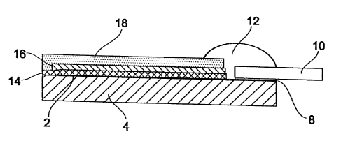
As can be seen in the embodiment of the present invention
shown in Fig_ 1, the patterned platinum layer, which is ap-
plied to a ceramic substrate 4 and which defines a platinum
thin-film resistor -2 as well as connecting areas 8, has
evaporated thereon an A1203 layer 14_ This layer 14 is evapo-
rated in such a way that it fully covens the platinum thin-
film resistor 2. On top of the evaporated layer 14 a further
layer 16 is arranged, which is formed by a ceramic paste that
has been applied e.g. by means of screen printing processes
and partially sintered. This layer 16 serves to reinforce
the previously evaporated A1203 layer. '.L'he layer 16 has then
applied thereto a glaze 18 in such a way that the platinum
film resistor 2 is sealed from the surroundings in a gastight
manner.
CA 02356856 2001-06-27
6
For producing the platinum temperature sensor according to
the present invention shown in Fig. 1, 'the A1203 layer 19 is
first evaporated onto the surface of the ceramic substrate 4,
on which the patterned platinum film layer is arranged, at
least in the area of the platinum film resistor 2. Making use
of a screen printing process, this layer 14 is then rein-
forced by a ceramic paste. Subsequently, the ceramic paste is
preferably partially sintered. The layer thickness of the
evaporated A1203 layer is in a range of prom 1 to 3 Vim, pref-
1o erably it is approx. 1.5 Vim. The above--mentioned reinforce-
ment of the intermediate layer by means of the ceramic paste
to a thickness of approx. 10 to 30 um is carried out for re-
alizing a reliable sealing also at high temperatures exceed-
ing 800°C. The ceramic paste can consist of a mixture of sev-
is eral ceramic powders and quartz powder, e.g. A1203, MgO,
Si02.
Following this, a glaze coating having a thickness of 30 to
200 ~tm is applied to the intermediate layer comprising the
2o two sub-layers 14 and 16 in the case of the preferred embodi-
ment. Also this glaze coating is preferably applied by means
of a screen printing process. Subsequently, a firing process
is carried out preferably at approx. 1,7.00°C so as to provide
for the platinum thin-film resistor .a protective coating
2s which is gas-tight with respect to the ambient atmosphere.
The structure shown in Fig. l in a schematic cross-section is
obtained in this way.