Note: Descriptions are shown in the official language in which they were submitted.
CA 02356999 2001-06-28
WO 00/42825 PCT/US00100024
ELECTROLUMINESCEN'r DEVICE AND
METHOD FOR PRODL;~CING SAME
FIELD
The present invention relates to an electroh:uninescent device (hereinafter
referred
to as "EL device") having a luminescent Layer which comprises luminescent
particles and
a binder resin. In particular, the present invention relates to an EL device
which can
achieve a high luminescent efficiency.
Back~,roany
EL devices having a so-called "dispersion t~~pe luminescent layer" which is
formed
by dispersing luminescent particles such as phosphor particles in binder
resins such as
polymers having a high dielectric constant are known from the following
publications.
For example, JP-B-59-14878 discloses an EL device comprising a transparent
substrate, a transparent electrode layer, an insulating layer consisting of a
vinylidene
fluoride binder resin, a luminescent layer comprising a vinylidene fluoride
binder resin
and phosphor particles, the same insulating layer as above, and a rear
electrode, which are
laminated in this order. JP-B-62-59879 discloses aua EL device comprising a
polyester
film, an ITO electrode, a Luminescent layer which c~ornprises phosphor
particles and a
cyanoethylated ethylene-vinyl alcohol copolymer (a binder resin) , and an
aluminum foil
(a rear electrode) , which are laminated in this order.
Unfortunately, however, it is difficult to increase the luminance in the case
of such
"dispersion type luminescent layers". The reason for this is that luminescent
particles,
which have a larger specific gravity than binder resins, tend to sink in a
coating for
forming luminescent layers comprising luminescent; particles dispersed in the
solution of
binder resins, and thus it is difficult to uniformly di:>perse the luminescent
particles in the
luminescent layers formed from such a coating. Fmvthermore, the dispersibility
deteriorates when the amount of luminescent particles in the coating is
increased to
increase the filling rate of luminescent particles in the luminescent layer.
The filling rate
of the luminescent particles is at most 20 volume % of the coating weight. In
addition, it
is relatively difficult to increase the coating thickne:;s of the luminescent
layer while
maintaining the uniformity of a thickness using such a dispersion type
coating. Therefore,
17-01-2001 CA 02356999 2001-06-28 VQv~ILS a t~,~= ~,;j OOOOOOO~
i'i.; ITUS ~U/U0024 - ~ PATcNTA~11J1~'~LT E
gIc.BE~T~ r i'~. a
Minnesota Mining and Manufacturing Company et al. g 1 ~~~ Iyi L.~ hl C E-~
Our Ref.: E 2091 PCT
9 7. J~;:. 2~~9 ~ .
when the number of applications of the coating is increased to increase the
thickness of the
luminescent layer, the productivity decreases, and it is diifficult to produce
a roll-form EL
device having a large area. -
..
EL devices having a "lamination type luminescent layer" are known as one
_ .5 measure to solve the drawbacks of the "dispersion type himinescent
layers". For example,
US Patent Nos..5,019,748 and 5,045,755 disclose an EL device having a
lamination type
luminescent layer, which consists of a three-Layer laminate comprising: (1} a
first
dielectric adhesive layer with a high dielectric constant aopIied on the
transparent 1
conductive layer of a transparent substrate; (2) a phosphor particle layer in
the. form of a
substantially single layer (having a thickness not exceeding the largest size
of particles),. .
which is formed by electrostatically applying dry phosph,~r panicles
(luminescent
particles) on the f rst dielectric adhesive layer; and (3} a second dielectric
layer placed on
the phosphor particle layer and containing a dielectric material with a high
dielectric
constant, which layer fills the spaces between adjacent phosphor particles. A
rear
electrode is applied on the surface of the second dielectric layer, and thus
the second
dielectric layer functions as an insulating layer.
Tn contrast with the above "dispersion type l~uininescent~layer",'itWs
possible to
continuously carry out the coating processes, and it is'pos;>ible to.produce a
roll-form EL
device by the disclosed method. However, the above publications and patent
?fl specifications do not disclose any specific manner to form a continuous
terminal bus
( s)~
through which electricity (voltage) may be applied from outside to the
transparent -
conductive layer, e:o., along the lengthwise direction of thf: transparent
substrate in the
. production process of a roll-form EL device.
. To increase the area of EL devices, it is a key factor.how a terminal (buss)
, which
supplies electricity (voltage} to a transparent conductive layer from the
outside is
r
promded. For example, in the case of EL devices for displays with a small
area, busses
which are not electrically in contact with a rear electrode, can be formed on
a trans are
p nt
conductive Layer by effectively repeating screen printing. I';[owever, none of
the above
cited publications or patents disclose the formation of busses continuously in
the
lengthwise direction of the device, or any methods for such formation.
<-> c ~ P~~- ~0.~ . .
2
AMENDED SHEET
CA 02356999 2001-06-28
WO 00/42825 PCT/US00/00024
Conventional "lamination type luminescent layers" have several drawbacks. For
example, EL devices having "lamination type luminescent layers" can emit light
at a
luminance equal to or higher than that of EL devices having "dispersion type
luminescent
layers" when they are connected with a power sotuce having the same frequency
and the
same voltage. However, the luminescent efficiency is not improved so greatly,
or
sometimes it may deteriorate.
Luminescent efficiency ("rl") is a value dE;fined by the following formula:
rl =Lx~cxS/P
where:
P is a used electricity (effective electric power) (unit: V~,
L is a luminance measured with a luminance meter (unit: cdlm2),
S is the area of a luminescent surface, and
~ is the ratio of the circumference of a circle to its diameter.
In other wards, a low luminescent efficiency means a low luminance per unit
effective
electric power, and thus a low power eff ciency. ,Accordingly, it is a goal to
improve the
luminescent efficiency from the viewpoint of energy-saving.
Summanr
In one embodiment, the present invention provides an EL device having an
effectively improved luminescent efficiency. Prei:erred such
electroluminescent devices
comprise:
a transparent conductive layer,
a binder layer placed on the back surface o~f the transparent conductive
layer,
a luminescent-particle Iayer comprising a :>ubstantially single layer of
particles
containing luminescent particles, which layer is applied on the back surface
of the
transparent conductive layer through the binder layer,
an insulating layer comprising insulating particles, which is placed on the
back
surface of the luminescent-particle layer, and
a rear electrode placed on the back surface of the insulating layer, wherein
the
luminescent particles are embedded in the binder layer, or the luminescent
particles are
substantially not embedded in the insulating layer.
3
17-01-2001 CA 02356999 2001-06-28 US 0000000
<US-A-4,143,297 refers to electroluminescerit information display panels which
are said to be suitable for uses extending from simple numeric displays to
color TV
panels. The display panel comprises a body of insulating resin having a layer
of
electroluminescent particles embedded therein. This layer is a monoparticle
layer.
The resin has a dielectric constant higher than that of the particles and
includes
fluorescent material on at least one side of .the layer of electroluminescent
particles. Furthermore, insulating coatings on both front and back surfaces of
the
resin body,. a transparent front electrode extending over the insulating
coating of
the front surface, a back electrode disposed on thE; insulating coating on the
back
surface and means for electrically energizing the f:lectrons are provided. At
least
one element of the display pane( adjacent the back thereof is black and
sufficiently
opaque to absorb substantially all the light reaching it.
WO 98/53645 refers to an electroluminescent device and a method for producing
the same. Among others the electroluminescent device comprises a luminescent
layer comprising a transparent support layer. comprising a matrix resin, 'an
insulating layer comprising an insulating material and a luminescent particle
layer
consisting essentially of particles which comprise luminescent particles and
which
are embodied in both the support layer and the insuiiating layer.>
AMENDED SHEET
CA 02356999 2001-06-28
WO 00/42825 PCTIUS00100024
In another embodiment, the present inventiion provides a method for the
production
of an EL device, which method can produce a sheet-form EL device having a high
luminescent efficiency at a high productivity without the use of the above
dispersion
coating.
Preferred methods for the production of an electroluminescent device (which
optionally comprise the features described above) comprise the steps of
applying a coating for the formation of a first layer of a binder layer on
either one
of the back surface of a transparent conductive layer and the surface of an
insulating layer,
placing particles containing luminescent particles iin a layer form on the
applied coating
prior to the solidification of the coating, and solidifying the coating after
partly embedding
the layer of the particles, to form the first layer of a binder resin and the
luminescent-
particle layer adhered to the first layer,
applying a coating for the formation of a second layer of a binder layer on
the
luminescent-particle layer, and solidifying the coating, to embed the
luminescent particles
I S in the binder layer consisting of the first and second layers without
exposing the surfaces
of the luminescent particles, and
applying the other of the transparent conductive layer and the insulating
layer on
the binder layer in which the luminescent particles are embedded.
In yet another embodiment, the present invention provides an EL device which
can
be produced in a roll-form from which a large-size luminescent device can be
easily
produced.
In this embodiment, the present invention provides an electroIuminescent
device as
described above; in which the transparent conductive layer, luminescent-
particle layer,
insulating layer and rear electrode preferably continuously extend along the
length of the
transparent conductive layer. The device further preferably comprises at least
one buss
which is electrically in contact with the back surface of the transparent
conductive layer,
has a width smaller than the width of the transparent conductive layer and
continuously
extends along the length of the transparent conductive layer, and the buss is
not
electrically in contact with the rear electrode.
One of the characteristics of the EL device <~ccording to one embodiment of
the
present invention is that luminescent particles are embedded in a binder
layer. 'Thereby,
4
CA 02356999 2001-06-28
WO 00/42825 PCT/US00/00024
the efficiency of luminance in relation to an effective electric power
(luminescent
efficiency) can be increased.
Although not intending to be bound by theory, the function of this structure
of an
EL device may be assumed as follows:
In conventional lamination type EL devices, spaces between phosphor
(luminescent) particles are filled with fillers having a very high dielectric
constant (e.g.
insulating particles, etc.). Thus, a capacitance in the spaces between the
phosphor particles
increases. Accordingly, a dielectric loss in such spaces increases, and/or an
electric power
is lost due to the generation of Joule heat. Therefore, the luminescent
efficiency
decreases.
In general, the dielectric constant of insulating particles is at least 100,
and typical
insulating materials having a relatively high insulating effect such as barium
titanate have
a dielectric constant of 1,000 or larger. In contrast with such insulating
particles, organic
polymers or high dielectric polymers, which can be used as binder resins
(sometimes
called as "matrix resins"), usually have a dielectric constant of less than
about 50, and
preferable high dielectric polymers such as vinylidene fluoride resins and
cyanoresins
have a dielectric constant of from about 5 to about 30. Herein, a dielectric-
constant is a
specific dielectric constant measured under the application of an alternating
current of 1
kHz, unless otherwise specified.
In the above construction of the present invention, luminescent particles are
preferably embedded in a binder resin layer, and preferably few (or more
preferably
effectively no) insulating particles having a very high dielectric constant
are present in
spaces between adjacent luminescent particles. Thus, the capacitance in such
spaces can
be effectively decreased.
One of the characteristics of an EL device according to another embodiment of
the
present invention is that luminescent particles are substantially not embedded
in an
insulating layer. When a luminescent-particle Layer is substantially not
embedded in an
insulating layer, fillers having a very high dielectric; constant (e.g.
insulating particles, etc.)
do not fill the spaces between the phosphor (Iumine;scent) particles, like in
the above
embodiment. Accordingly, it is possible to suppress the increase of a
dielectric loss and
the electric power loss due to the generation of Joule heat in such spaces as
much as
possible, and thus a luminescent efficiency can increase. Such a structure can
be easily
5
CA 02356999 2001-06-28
WO 00/42825 PCT/US00/00024
formed, for example, by embedding luminescent particles in a binder layer,
like in the
above case, so that the particle surfaces do not expose on the back surface of
the binder
layer which is in contact with the insulating layer.
Characteristics of an EL device in one prejPerred embodiment of the present
invention are that a transparent conductive layer, a luminescent-particle
layer, an
insulating layer and a rear electrode continuously extend along the lengthwise
direction of
a transparent electrode layer, and that the device fiurther comprises at least
one buss which
is electrically in contact with the back surface of tlhe transparent
conductive layer and has a
width smaller than the width of the transparent conductive layer and
continuously extends
along the lengthwise direction of the transparent electrode layer. Another
preferred
characteristic is that the buss is not electrically in contact with the rear
electrode. Thus, it
is possible to produce a roll-form EL device, from which a large-sized
luminescent display
can be easily formed.
When a buss is not in direct contact with a luminescent layer, it becomes more
easy to form a roll-form EL device having a large .area, since a rear
electrode can be
applied onto substantially the whole back surface of the luminescent layer,
and thus
substantially the whole surface of the luminescent layer can emit light.
For example, a buss can be in direct contact with the edge area of a
luminescent
layer. However, in this case, the buss and an electrode-free area in which no
rear electrode
is applied should be provided on the back surface of the luminescent layer to
separate the
rear electrode and the buss, so that the buss and rear electrode are not
electrically in
contact with each other. A part of the light-emitting surface of the
luminescent layer,
which corresponds to the electrode-free area, can emit substantially no light,
and thus the
light-emitting area may not be increased.
The EL device of the present invention can be produced by various methods. For
example, it is preferably produced by a method, which comprises the steps of
applying a coating for the formation of the first layer of a binder layer on
either
one of the back surface of the transparent conductive layer and the surface of
the
insulating layer, placing particles containing luminescent particles in a
layer form on the
applied coating prior to the solidification of the coating, and solidifying
the coating after
partly embedding the layer of the particles, to form the first layer of a
binder resin and the
luminescent-particle layer adhered to the first layer,,
6
CA 02356999 2001-06-28
applying a coating for the formation of the second layer of a binder layer on
the
luminescent-particle layer, and solidifying the coating, to embed the
luminescent particles
in the binder layer consisting of the first and second layers without exposing
the surfaces
of the luminescent particles, and
applying the other of the transparent conductive layer and the insulating la
er on
y
the binder layer in which the luminescent particles are embedded.
The above method can produce an EL device having an improved luminescent
efficiency at a good productivity. Furthermore, a sheet-~forrn EL device
having a large
area or a roll-form EL device can be easily produced.
Working Embodiments of the Invention .
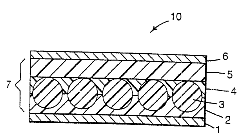
An EL device 10 according to one embodiment of the present invention is show
t
in FIG. 1 and comprises a transparent conductive ~yer;Yl in close contact with
a
transparent substrate (not shown), a rear electrode~.6r, arid a luminescent
layer x! which is
I ~ placed between the transparent conductive layer and the rear electrode.
In one embodiment, the luminescent Iayer;Y' cornprises a first layer ~ of the
3
binder layer, a. luminescent-particle layer~3' comprising luminescent
particles which are in
close contact with the first Layer of the binder layer so th;~t they are
partly embedded in the
rust layer. while remaining parts of the particles are exposed, a second layer
~'of the
binder layer which is in close contact with the luminescent-particle layer to
coyer the
S
e:cposed remaining parts of the luminescent particles, ancL an insulating
layer which is
4
in close contact with the second Iayer~'of the binder layer.
Es ~- _
In the embodiment of FIG. 1, the rear electrode~(fahd the insulating layerk$
are
preferably in contact with each other, and their contact surfaces are
preferably
substantially flat.
3
In the embodiment of FIG. 1, the luminescent-particle layer~is preferably
completely embedded in the binder layer comprising a birder resin and is not
in contact
~S:
with the insulating Iayer~3'containing insulating particles, or the
luminescent particles are
in point contact with the insulating layer, that is, most of the luminescent
particles (those
having relatively large particle sizes, etc.) are in point contact with the
insulatin . Ia er.
g Y
but, few and preferably no insulating particles are, present in the spaces
between the '
adjacent luminescent particles. The opposing surfaces of the insulating layer
and ~ .
7
AMENDED SHEET
CA 02356999 2001-06-28
WO 00/42825 PCT/US00100024
transparent conductive layer are substantially paraallel .with each other and
substantially
flat. Such a structure is advantageous to increase .a luminescent efficiency.
If desired, the transparent conductive layer and luminescent layer may be in
contact with each other. In such a case, a luminance can be effectively
increased. In
general, an interface between the insulating layer and rear electrode is
substantially flat.
The whole thickness of an EL device is usually in the range of 50 to 3000 pm,
and
the length of an EL device is usually at least 1 m, when if is in the roll
form.
Preferably, the width of a transparent conductive layer is wider than that of
a
luminescent layer, and at least one buss is formed in the area of the
transparent conductive
. layer in which no Luminescent layer is formed, though not shown in the
figure. In this
case, the buss is not in direct contact with the luminescent layer; or not in
electrically
contact with the rear electrode. In such a structure, busses are usually
applied near the
lengthwise edges of the transparent conductive Layer in the form of two
stripes, which are
substantially in parallel with the luminescent layer carrying the rear
electrode.. .~
The shape and arrangement of a buss are not limited to those described above,
insofar as the buss functions as a terminal for supplying an electricity
(voltage) to a
transparent conductive layer from outside. For example, a buss may consist of
a plurality
of small buss parts which extend in the form of a bar code in the lengthwise
direction, or a
plurality of circular buss parts which are present along the length of the
device. That is,
small busses may discontinuously exist in the lengthwise direction, insofar as
the busses as
a whole continuously extend.
For example, when an EL device for a large;-sized display is formed by cutting
a
desired Length from the stock product of an EL device, a luminescent Layer
should be
present on a transparent conductive layer with no discontinuous part, while
adjacent buss
parts may be discretely present insofar as the buss parts can function as
terminals for
supplying an electricity (voltage) to a transparent conductive layer from the
outside.
A buss may be formed from a conductive rr~aterial by an application method,
which can be employed also in the formation of a near electrode. The
application method
is preferably the application of a coating containing a conductive material,
vapor
deposition, sputtering, ete., since a buss, which continuously extends along
the lengthwise
direction of a transparent substrate, can be easily formed in the production
method of a
roll-form EL device.
8
CA 02356999 2001-06-28
WO 00/42825 PCT/US00/00024
As explained above, an EL device of one preferred embodiment of the present
invention is characterized in that luminescent particles are embedded in a
binder layer, and
no insulating particles are present in spaces between adjacent luminescent
particles.
Accordingly, a luminescent efficiency can be increased. That is, the spaces
between the
phosphor particles are filled with a binder resin containing no insulating
particles. In such
a case, the luminescent-particle layer is substantially not embedded in the
insulating Layer.
The term "substantially not embedded in an insulating layer" means that (~) a
luminescent-particle layer is not in contact with are insulating layer, (2) a
luminescent-
particle layer is in point contact with an insulating layer, or (3) a
luminescent-particle layer
is in contact with an insulating layer while no insulating particles are
present in the spaces
between the adjacent luminescent particles. In the cases ( i ) and (2), the
opposing surfaces
of the insulating layer and transparent conductive layer are substantially in
parallel with
each other, and substantially flat.
Furthermore, Inminescent particles having a relatively wide particle size
distribution may be used, so that a part of the Iumi:nescent particles are
embedded in an
insulating layer insofar as the effects of the present invention are not
impaired.
A particle size distribution can be defined as follows:
The percentage of particles having a particle size of not exceeding 5 times
the
average particle size is usually at Least 85 % preferably at least 90 %, and
more preferably
at least 95 %, based on the whole particles. The percentage of particles
having a particle
size of a half or less of the average particle size is usually at least 1 %,
preferably at least 2
%, in particular from 3 % to 25 %, based on the whole particles.
Particle sizes can be measured with a scanning electron microphotograph (SEM
photograph). In the case of non-spherical particles, the particle size of each
particle is the
average of the largest size of the particle (e.g. the major axis of an
ellipsoid) and the
smallest size of the particle (e.g. the minor axis of an ellipsoid) observed
in a SEM
photograph.
As explained in the above, the dielectric coefficient of insulating particles
is
usually at least 100, while that of binder resins is usually less than 50. In
the above
structure, luminescent particles are embedded in a binder layer, but they are
substantially
not embedded in an insulating layer. Thus, a capacitance in the above spaces
can be
effectively decreased.
9
CA 02356999 2001-06-28
WO 00/42$x5 PCTIUS00/00024
To effectively decrease the capacitance in the above spaces, a binder layer
may
optionally be separated in two layers; a luminescent-particle layer in the
form of a single
layer is formed so that a part of the luminescent-particle layer is embedded
in the first
layer of the binder layer, and the second layer of the binder layer is applied
to cover the
exposed part of the luminescent-particle layer, whereby the luminescent-
particle Iayer is
embedded in the binder layer consisting of the first and second layers,
without exposing
the surfaces of the luminescent particles. In this case, the first and second
layers contain
substantially no insulating particles.
Suitable polymers which can be used as binder resins include THV
(tetrafluoroethylene-hexafluaropropylene-vinylide:ne fluoride copolymers),
etc.
When a binder layer has two or more layers, a binder resin in a layer facing
an
insulating layer preferably has an as small dielectric constant as possible
and/or an as
small dielectric tangent as possible. For example, the dielectric constant of
a binder resin
in a.layer. on an insulating layer side is usually 20 car less,-preferably
l5~or less, in .
particular from 1 to 10.
A dielectric constant may be decreased by the addition of glass bubbles (glass
balloons or hollow particles) to the layer of a binder layer on the insulating
layer side to
fill minute bubbles. In this case, the diameter of a bubble is preferably
smaller than the
particle size of luminescent particles, and is usually 10 ~m or less.
A luminescent-particle layer in the form of a substantially single layer maybe
formed from a coating (slurry) containing a binder resin such as a high
dielectric polymer,
and luminescent particles dispersed in such a binder resin. In this case, for
example, a
curtain coating method is employed to reduce the tr~ickness of the coating
without the
application of any shear on the coating, and to form a luminescent layer
having
substantially the same thickness as the particle size of the luminescent
particles. The
coating procedure which applies no shear on the co<~ting can easily form a
luminescent
layer which is continuous in the lengthwise direction. The coating (coated f
lm) can be
solidified by any conventional method such as drying, cooling, curing, etc.
When a luminescent Layer comprises a luminescent-particle layer, a binder
layer
and an insulating layer, a luminance can be increased in comparison with that
of the
conventional dispersion type EL devices. That is, tree problems, which may be
caused by
the sink of the luminescent particles in a coating for forming a luminescent
Iayer, are not
CA 02356999 2001-06-28
WO 00!42825 PCT/US00/00024
caused, unlike the "dispersion type luminescent layers", since an insulating
layer and a
binder layer can be formed from coatings containing few or more preferably no
luminescent particles. Therefore, the filling rate of luminescent particles in
a luminescent-
particle layer can be very easily increased, and can reach a substantially
close-packed
state, for example, at least 60 %, and thus a luminance and luminescent
efficiency can be
easily improved. An EL device having such a luminescent-particle layer is
preferable
from the viewpoint of the production of a roll-form EL device having a large
area. In
addition, it is very easy to form a luminescent layer which continuously
extends in the
lengthwise direction. The luminescent-particle layer of a luminescent layer
having such a
structure can be formed by a powder-coating method, for example, scattering of
luminescent particles, the details of which will be explained below.
An EL device having such a luminescent-particle layer is preferably produced
by
the following method.
Firstly, a coating for forming the first layer of a binder Layer is applied on
the back
surface of a transparent conductive layer which hays been formed on the back
surface of a
transparent substrate, and particles containing luminescent particles are
scattered in the
form of a layer on the coating prior to the solidification of the coating.
After partly
embedding the layer of particles in the coating, thc~ coating is solidified to
form the first
layer of a binder layer, and a luminescent-particle layer which is partly
embedded in the
first layer.
Then, a coating for forming the second layer of the binder layer is applied on
the
above luminescent-particle layer, and solidified to embed the luminescent-
particle layer in
the binder layer consisting of the first and second layers without exposing
the surfaces of
the luminescent particles.
The coating of the first and second layers may be carried out by various
methods,
including, for example, roll coating, bar coating, knife coating, die coating
or curtain
coating. These coating methods can easily achieve the embedding of the
luminescent-
particle layer and the smoothening of the surface of the binder layer.
Subsequently, an insulating layer is applied. an the binder layer (the back
surface
side} in which the luminescent-particle layer is em3bedded. The insulating
layer is
preferably formed by applying a coating for an insulating layer containing a
resin and
11
CA 02356999 2001-06-28
WO 00/42825 PCT/US00/00024
insulating particles dispersed in the resin on the back surface of the binder
layer, and
drying it.
Finally, a rear electrode is applied on the back surface of the insulating
layer to
finish the EL device of the present invention.
Alternatively, it may be possible to emplo.~ anther method in which the layers
are
formed in the reverse order. That is, firstly, the second layer of a binder
layer, a
luminescent-particle layer and the first layer of the binder layer are
laminated on the
smoothened surface of an insulating layer which has been formed on a rear
electrode, and
finally a transparent conductive layer (or a transparent substrate carrying a
transparent
conductive layer) is laminated.
The above methods can very easily produce an EL device having an improved
luminescent efficiency continuously at a high rate, namely, at a high
productivity. For
example, an EL device can be produced at a coating rate of at least 5 mpm
(m/min.),
preferably from I0 to 200 mpm, in particular from 12 to 100 mpm.
The amount of luminescent particles in the particles contained in the
luminescent-
particle layer is preferably at least 40 volume %. V4~hen the amount of the
luminescent
particles is less than 40 volume %, the effects to improve the luminance and
luminescent
effect may deteriorate. The luminance and luminescent effect are maximized
when the
particles consist of luminescent particles. Thus, the particularly preferable
amount of the
luminescent particles contained in the phosphor particle layer is from 50 to
100 volume %.
An insulating layer may be placed at a certain distance (space) from a
luminescent-
particle layer and a binder layer, so that the luminescent particles are
substantially not
embedded in the insulating layer. In this case, the ;surfaces of the
luminescent particles
may be exposed on the binder layer. That is, the surfaces are exposed in an
air layer
(space) formed between the insulating layer and binder layer. Such a structure
may be
formed by providing spacer elements discretely on the back surface of the
binder layer in
which the luminescent particles are partly embedded, and bonding the
insulating layer to
the spacer elements. in this case, the surfaces of the luminescent particles
are exposed in
an air layer (air rooms) surrounded by the binder layer, spacer elements and
insulating
layer. In such a structure, the luminescent particles are substantially not
embedded in the
insulating layer.
12
CA 02356999 2001-06-28
WO 00/42825 PCT/US00/00024
As explained in the above, the preferred embodiment of the present invention
provides an EL device which can be produced in a roll form. In a roll-form EL
device, a
transparent conductive layer, a luminescent layer (comprising a binder layer,
a
luminescent-particle layer which is bonded to the transparent conductive layer
through the
binder layer, and an insulating layer), a rear electrode and a buss are placed
on a
transparent substrate, which continuously extends in the lengthwise direction,
and they
continuously extend along the lengthwise direction of the transparent
substrate. Thus, it is
very easy to obtain an EL device having a luminescent layer with a large-area
(plane size),
etc., which continuously extend in the lengthwise direction. That is, a roll-
form EL device
having a luminescent layer extending in the Iengtl:~wise direction is produced
and stored as
a stock product. Then, an EL device having a desired length can be obtained by
cutting
such a length from the stock product of an EL device.
The conventional production methods using screen printing can form laminated
parts such as a luminescent layer, a buss, etc. on a. transparent substrate
discontinuously in
the lengthwise direction. A conventional stock product of EL devices which are
produced
by screen printing can provide only EL devices having a size {length) which
does not
include the above discontinuous part. In contrast, when the roll-form EL
device of the
present invention is used as a stock product, it can be applied to products
having various
sizes, as explained in the above.
A roll-form EL device is preferably produced by a method comprising the
following steps:
providing a transparent substrate on one suxface of which a transparent
conductive
layer is applied;
forming a luminescent layer by placing a binder layer a luminescent-particle
layer
and an insulating layer on the transparent conductive layer so that the width
of the
luminescent layer is smaller than that of the transparent conductive;
placing a masking on the exposed part of the transparent conductive layer of
the
luminescent layer-carrying substrate, that is, a luminescent layer-free area,
in the
lengthwise direction of the transparent substrate, v~rhere the masking has a
width smaller
than that of the luminescent layer-free area; and
applying a conductive material onto the Iunninescent layer-carrying substrate
to
form a rear electrode and a buss which is electrically in contact with neither
the
13
CA 02356999 2001-06-28
WO 00/42825 PCT/US00/00024
luminescent Layer nor the rear electrode due to th.e presence of the masking
or an exposed
part from which the masking is removed.
One of the characteristics of this method its that the rear electrode and buss
preferably can be formed so that the buss is in direct contact with neither
the luminescent
layer nor the rear electrode due to the presence of (1) the masking or (2) the
exposed part
of the transparent conductive Layer from which the masking has been removed,
and on
which no luminescent layer has been applied.
In this method, a masking may be removed if desired. It is not necessary to
remove a masking insofar as a buss is not electrically in contact with a rear
electrode. For
example, a masking is not removed, when the first conductive material which
forms a rear
electrode and the second conductive matexial which forms a buss are applied at
the same
time but with different application apparatuses, or in different steps, and a
masking
prevents the rear electrode and the buss, which are formed from two conductive
materials,
from being in contact each other. Furthermore, a masking is not removed, when
the
thicknesses of a luminescent layer and a masking are sufficiently large in
comparison with
the thickness of a buss to be formed, and conductive materials, which are
applied at the
same time, can be separated between a buss-forming area and a rear electrode-
forming
area. However, a masking is preferably removed, since a rear electrode and a
buss, which
are not electrically in contact each other, can be easily formed.
The first and second conductive materials may be the same or different.
However,
a buss and a rear electrode are preferably formed apt the same time, since the
production
steps can be simplified, and the productivity increases.
A roll-form EL device having high luminance and a Large area can be produced
at a
high productivity, when the EL device is produced by a method comprising the
following
steps:
providing a transparent substrate on one swrface of which a transparent
conductive
layer is applied;
placing a masking on the surface of the trar.~sparent conductive layer to
cover a
buss-forming area, on which a buss will be formed., with the masking, so that
a buss-
forming area having the applied masking and a masking-free area having no
masking are
formed on the transparent conductive layer;
14
CA 02356999 2001-06-28
w0 00/42825 PCT/US00/00024
placing a luminescent layer on the masking-free area of the transparent
conductive
Layer to form a luminescent layer carrying substrate; and
applying a conductive material onto the l~uninescent layer-carrying substrate
to
form the rear electrode on the luminescent layer, :removing at least a part of
the masking to
expose the buss-forming area, and then applying a conductive material onto the
exposed
buss-forming area, to form the rear electrode and the buss which is
electrically in contact
with neither the luminescent layer nor the rear electrode due to the presence
of the
masking or the exposed part from which the masking is removed.
One of the characteristics of this method is that a masking is applied on a
transparent conductive layer prior to the application of a luminescent layer
to form a buss-
forming area having the applied masking, and a masking-free area having no
masking.
This method can easily prevent the damage of the buss-forming area on the
transparent
conductive layer due to scratching, etc. from the step of the formation of a
luminescent
layer to the step of the formation of a buss. In thi:~ case, a masking makes
it easy to form a
continuous buss in the lengthwise direction of the substrate, and functions as
a protective
film of a transparent conductive layer (in the buss-forming area).
In this method, a masking is removed, and it may be removed partly or wholly.
For example, in the applying step, the first conductive material is applied on
a luminescent
layer-carrying substrate, and at least a part of the masking is removed to
expose a buss-
forming area. Then, the second conductive material is applied on the exposed
buss-
forming area to form a buss. Alternatively, when a part of the masking is
removed and
then the second conductive material is applied to the exposed buss-forming
area, the
remaining masking may be removed if necessary. Preferably, the whole masking
is
removed, since a rear electrode and a buss, which ~~re not electrically in
contact each other,
can be easily formed. The first and second conductive materials may be the
same or
different.
When a masking is utilized as the protective film of a transparent conductive
layer,
preferably a part of the masking is removed in the applying step to expose a
buss-forming
area, and then the conductive material is applied on. the luminescent layer-
carrying
substrate to form, at the same time, a rear electrode and a buss which is
electrically in
contact with neither the luminescent layer nor the rear electrode, since the
rear electrode
CA 02356999 2001-06-28
WO 00/42825 PCT/US00/00024
and the buss, which are not electrically in contact: with each other, can be
particularly
easily formed, and thus the production steps can be simplified.
The above buss is preferably formed by any application method of a conductive
material (e.g. application of a coating liquid, vapor deposition, sputtering,
etc.). Thereby, a
buss, which extends continuously along the lengtihwise direction of the
substrate, can be
particularly easily formed in the production proceas of a roll-form EL device.
Conductive
materials, which are used to form a buss and a rear electrode will be
explained below:
As masking materials, repeelable adhesive; tapes such as masking tapes,
application
tapes for sealing, etc., repeelable resin coatings, and the like, which are
used in general
coating methods, can be used.
The thickness of a masking is usually from 0.1 to 100 p.m. The preferable
thickness of a masking is from 0.1 to 30 ~tm, when a masking is used as-the
protective
f Im of a transparent conductive layer (in a buss-forming area).
Now, the component elements used in the ;present invention will be explained
in
detail.
A transparent substrate is preferably used as the support of a transparent
conductive layer. The transparent substrate may be a glass plate, a plastic
film, etc., which
is used in the conventional dispersion type EL devices.
Examples of suitable plastic films used as substrates are films of polyester
resins
such as polyethylene terephthalate (PET), polyethylene naphthalate (PEN),
etc.; acrylic
resins such as polymethyl methacrylate, modified polymethyl methacrylate,
etc.;
fluororesins such as polyvinylidene fluoride, acryl-modified polyvinylidene
fluoride, etc.;
polycarbonate resins; vinyl chloride resins such as vinyl chloride copolymers;
and the like.
The transparent substrate may be a single layer film, or it may be a
multilayer film.
For example, the whiteness of the light can increase, when at least one layer
of the film or
multilayer film has high transparency and contains a dye which develops a
complimentary
color to a color emitted by the luminescent layer. Preferably, examples of
such a dye are
red or pink phosphor dyes such as rhodamine 6G; r:hodamine B, perylene dyes,
etc. when
the emitted light from the luminescent layer is blue-green. Furthermore,
processed
pigments comprising these dyes dispersed in resins may be used.
16
CA 02356999 2001-06-28
WO 00!42825 PCTNS00100024
Preferably both surfaces of the transparent substrate are usually flat, while
the
surface which is not in contact with the transparent conductive layer may have
prismic
projections unless the effects of the present invention are impaired.
The light transmission through the transparent substrate is usually at least
60 %,
preferably at least 70 %, in particular at least 80 °ro. Herein, the
"light transmission" means
the transmission of light measured using a UV-lig;ht/visible light
spectrophotometer "U
best V-560" (manufactured by NIPPON BUNI~O KABUSHKIKAISHA) with light of 550
nm.
The thickness of a transparent substrate is usually between 10 and 1000 ~,m
when a
roll-form EL device is formed.
A transparent substrate may contain additives such as UV light absorbers,
moisture
absorbents, colorants, phosphor materials, phosphors, and the like unless the
effects of the
present invention are impaired.
A transparent conductive layer preferably i.s placed on the back surface of
the
1 S transparent substrate in close contact therewith. The transparent
conductive layer may be
any transparent electrode which is used in the dispersion type EL devices such
as an ITO
{Indium-Tin Oxide) film, and the like. The thickness of the transparent
conductive layer is
usually between 0.01 and 1000 p.m, and the surface resistivity is usually 500
S2/square or
less, preferably between l and 300 S2/square. The light transmission is
usually at least 70
%, preferably at least 80 %.
Suitable ITO film is formed by any conventional film-forming method such as
vapor deposition, sputtering, paste coating, and the like. The ITO film
optionally is
formed directly on the transparent substrate, while a primer layer may be
formed on the
transparent substrate, and then the ITO film may bc~ formed on the primer
layer. The
thickness of a primer is usually between 0. 1 and 100 p,m. In place of the
primer layer, the
surface of the transparent substrate is treated with corona, and the like to
facilitate the
adhesion of the ITO film. Alternatively, the ITO film is formed on a
luminescent layer
and then a transparent substrate is laminated on the ITO film.
Alternatively, an ITO film, which has been formed on the release surface of a
temporary substrate, is transferred to the back surface of a transparent
substrate through a
transparent adhesive. As a temporary substrate, a release paper, a release
film, a low
density polyethylene film, etc. can be used.
17
CA 02356999 2001-06-28
WO 00/42825 PCT/US00/00024
A rear electrode layer preferably is placed on the back surface of a
luminescent
layer, that is, the side facing an insulating layer. The rear electrode is in
direct contact
with the luminescent layer in the embodiment of Fig. 1.
A resin layer can be provided between thc: rear electrode and the luminescent
layer
to increase the adhesion between them. A resin for the resin layer may be the
same resin
as a binder resin, which will be explained below. The resin layer may contain
insulating
organic particles.
A rear electrode may be a conductive filrr.~ used in the dispersion type EL
devices
such as a metal film of aluminum, gold, silver, copper, nickel, chromium,
etc.; a
transparent conductive film such as an ITO film; a conductive film such as a
conductive
carbon film; and the like. Such a conductive material film is preferably
formed by the
application of a coating containing a conductive material (e.g. bar coating,
spray coating,
curtain coating, etc.), vapor deposition, sputtering;, and the like. The metal
film may be a
vapor deposited film, a sputtered film, a metal foil, and the like. Also, an
electrode film
comprising a substrate (e.g. a polymer film, etc.) carrying a conductive layer
can be used
as a rear film.
The thickness of the rear electrode is usualLly between 5 nm and 1 mm.
The EL device can emit light from both surfaces when the rear electrode
consists
of a transparent conductive film and also the insulating layer is transparent.
A binder layer is placed preferably on the lback surface of a transparent
conductive
layer in close contact therewith, and thereby the iurninescent efficiency of
the luminescent
layer is easily increased. The binder layer preferalbly is a transparent layer
containing a
binder resin: The thickness of each of the first and second layers of the
binder layer is
usually between 0.5 and 1000 p,m, and the light transmission is usually at
least 70 %,
preferably at least 80 %. The total thickness of the: binder layer
{irrespective of a single
layer or a multilayer having two or more layers) is usually from 1.0 to 2000
p,m, and the
light transmission is usually at least 70 %, preferat~ly at least 80 %.
A binder resin may be a high dielectric polymer, a polymer having a relatively
low
dielectric constant (for example, less than 5), etc. 'The polymers having the
high dielectric
constant are those having a dielectric constant of usually at least about
S,.preferably
between 7 and 25, more preferably between 8 and 18. When the dielectric
constant is too
18
CA 02356999 2001-06-28
WO OOI42825 PCT/US00/00024
low, the luminance may not increase. When it is too high, the luminescent
efficiency may
not increase.
Examples of the polymers having the high dielectric constant are vinyIidene
fluoride resins (e.g. the above-described THV, etc~.) , cyanoresins,
polyvinylidene chloride
resins, and the like, and mixture of two or more of them. For example, the
vinylidene
fluoride resin may be obtained by copolymerization of vinylidene fluoride and
at least one
other fluorine-containing monomer. Examples of the other fluorine-containing
monomer
are tetrafluoroethyIene, trifluorochloroethylene, h~exafluoropropylene, and
the like.
Examples of the cyanoresin are cyanoethylcellulose, cyanoethylated ethylene-
vinyl
alcohol copolymer, cyanoethylpullulan, cyanoetylated polyvinyl alcohol, and
the like.
A binder layer usually consists of a binder resin, while it may contain
additives
such as other resins, fillers, bubbles, hollow or solid minute glass
particles, surfactants,
UV light absorbers, antioxidants, antifungus agent,, rust-preventives,
moisture absorbents,
colorants, phosphors, and the like, unless the effects of the present
invention are impaired.
I 5 For example, the binder layer may contain red or pink phosphor dyes such
as rhodamine
6G, rhodarnine B, perylene dyes, and the like, when the emitted light from the
luminescent-particle layer is blue-green. Furthermore, the above other resins
may be
curable or tacky.
In addition, a layer of a binder layer, which is provided on the insulating
layer side,
may contain bubbles or minute hollow glass particles to decrease the
dielectric constant of
the binder layer.
An insulating layer in a luminescent layer is essential to effectively prevent
the
dielectric breakdown of the luminescent layer. Insulating materials contained
in the
insulating layer may be the ones having a dielectric. constant of 100 or
larger, such as
inorganic insulating particles, which are used in the; conventional dispersion
type EL
devices.
The insulating layer is usually a coating layer formed from a coating which
has
been prepared by dispersing the insulating particles in a resin. The resin of
the insulating
layer is preferably a polymer having a high dielectric constant, which can he
used in a
binder layer.
Examples of the insulating particles are insulating inorganic particles of,
for
example, titanium dioxide, barium titanate, and the like.
19
CA 02356999 2001-06-28
WO 00/42825 PCTIUS00/00024
The insulating layer may be formed by the application of a coating on either a
rear
electrode or a binder layer in which a luminescent-particle layer is embedded.
When the insulating layer is a coating layer comprising insulating particles
and a
polymer having a high dielectric constant, the amount of the insulating
particles is
between 1 and 400 wt. parts, preferably between :l0 and 350 wt. parts, more
preferably
between 20 and 300 wt. parts, per 100 wt. parts ojPthe polymer having the high
dielectric
constant. When the amount of the insulating partiicles is too low, the
insulating effect
decreases, and the dielectric breakdown may occur when a relatively high
voltage is
applied. When the amount is too high, the application of the coating may be
difficult.
The thickness of the insulating layer is usually between 2 and 1000 pm. The
insulating layer may contain additives such as fillers, surfactants,
antioxidants, antifungus
agents, rust-preventives, moisture absorbents, colorants, phosphors, curable
resins,
tackifiers, and the like, insofar as the insulating pr~~perties are not
impaired.
Luminescent particles in a luminescent particle layer spontaneously emit light
when they are placed in an alternating electric field. As such the particles,
phosphor
particles which are used in the luminescent layer of the dispersion type EL
devices can be
used. Examples of the phosphor materials are single substances of phosphor
compounds
(e.g. ZnS, CdZnS, ZnSSe, CdZnSe, etc.), or mixtures of the phosphor compounds
and
auxiliary components (e.g. Cu, I, CI, Al, Mn, NdF3, Ag, B, etc.). The average
particle
size of the phosphor particles is usually between 5 and 100 pm. Particulate
phosphor
materials, on which the coating film of glass, cerannics, and the like is
formed, may be
used.
The thickness of the luminescent particle layer is usually between 5 and 500
p.m.
When the phosphor particle layer consists of a plurality of particles which
are placed in a
single layer state, the EL device can be made thin easily.
Furthermore, the luminescent particle layer may contain at least two kinds of
luminescent particles. For example, at least two kinds of luminescent
particles which emit
blue, blue-green, green or orange light and have discrete spectra each other
are mixed, and
thus a luminescent layer having the high whiteness can be formed.
The luminescent particle layer may contain one or more kinds of particles
other
than the luminescent particles, for example, particle, of glass, coloring
materials,
phosphors, polymers, inorganic oxides, and the like. For example, luminescent
particles
CA 02356999 2001-06-28
WO 00/42825 PCT/US00/00024
which emit blue-green light and a pink-coloring material which is the
complimentary color
to blue-green (e.g. particles containing rhodamine; 6G; rhodamine B, perylene
dyes, etc.)
are mixed f or forming the luminescent layer having the high whiteness.
The laminate structure of a luminescent layer comprising a binder layer, a
luminescent particle layer and an insulating layer :may be formed as follows:
Firstly, a luminescent-particle layer is formed on the surface of a
transparent
conductive layer by any conventional powder coating method. For example, a
binder
layer is applied on the back surface of a transparent conductive layer, and
then particles
containing luminescent particles are scattered on the binder layer while it
maintains
flowability, by a suitable method such as static suction, spraying,
gravirnetric scattering,
and the like, sa as to completely embed the particles in the binder layer.
After that, the
flowability is deprived of from the binder layer, and the binder layer and
particle layer are
bonded.
When a binder layer consists of two layers, a luminescent particle layer is
formed
so that the particles are partly embedded in the f rst layer, and then the
flowability is
deprived of from the first layer, so that the binder layer and particle layers
are bonded.
Then, the exposed surfaces of the luminescent particles are completely covered
with the
second layer to form the luminescent-particle layer embedded in the binder
layer.
For maintaining the flowability of the binder layer, the following methods are
preferable: a method for maintaining the undried state of a coating layer
formed from a
coating for a binder layer containing a solvent, a method for maintaining a
binder layer at
a temperature higher than the softening or melting point of a resin for a
binder layer, and a
method for adding a radiation-curable monomer or oligomer to a coating for a
binder
layer. These methods make a solidifying procedure. for suppressing the
flowability of the
binder layer (drying, cooling or hardening) easy.
An insulating layer is then laminated on the binder layer which has been
formed as
above, and a laminate structure in which they are bonded is formed. The
insulating layer
is preferably laminated by applying a coating containing materials for forming
the
insulating layer and solidifying it, or by press-bonding a film made of
materials for
forming the insulating layer. These methods can swrely form a luminescent
layer having a
high durability, in which a binder layer, a luminescent-particle layer and an
insulating
layer are closely bonded.
21
CA 02356999 2001-06-28
WO 00/42825 PCTNS00/00024
In the luminescent-particle Iayer formed as above, the binder resin penetrate
in
spaces between the particles. In such a case, the fvilIing rate of particles
is usually at least
20 volume %, preferably at Ieast 30 volume %, more preferably at least 40
volume
since the decrease of the filling rate may lead to tlye decrease of luminance
and
luminescent efficiency.
Herein, the "filling rate of particles" is defined as a percentage of the
total volume
of the particles in the volume of a hypothetical layer comprising all the
particles in the
luminescent particle layer and the materials which are present between the
particles.
Furthermore, an insulating layer may be the laminate of two or more layers,
unless
the effects of the present invention are impaired.
Now, the production method of one preferable example of an EL device as a
whole
according to the present invention will be explained.
Firstly, a transparent substrate, on which buck surface a transparent
conductive
layer has been laminated, is provided, and a binder layer containing an
embedded
luminescent-particle layer is applied to the back surface of the transparent
conductive
layer.
In general, the back surface of the transparent conductive layer is made
substantially flat.
When a binder layer consists of two or more layers, the particles are embedded
in
one of the layers of the binder layer so that usually 1 to 99 %, preferably 10
to 90 %, more
preferably 20 to 80 % of the size of each particle in the vertical direction
(to the plane of
the support layer) , fvr example, the diameter of a slpherical particle, is
embedded in the
support layer. When the embedded percentage is less than 1 %, the particle
layer tends to
be damaged during the formation of other layer of tlhe binder layer. When the
particles are
embedded so that the embedded percentage exceeds. 99 %, the particle layer may
not be
uniformly formed in the form of a single layer.
The binder layer is formed so that it has a width smaller than that of a
transparent
conductive layer, when a buss is applied.
The coating thickness of the coating for forming the binder layer is selected
so that
the dry thickness of the binder Iayer is in the above range. The solid content
in the coating
for forming the binder layer is usually between 5 and 80 wt. % when the binder
layer is a
single layer or a multiiayer. Suitable solvents used in the coating are
selected from
22
CA 02356999 2001-06-28
WO 00/42825 PCT/US00/00024
conventional organic solvents and mixtures of solvents, and preferably are
selected so that
the binder resin is effectively homogeneously dissolved.
The coating may be prepared with mixing or kneading apparatuses such as homo-
mixers, sand mills, planetary mixers, and the like.
For applying the coating, coating apparatuses such as bar coaters, roll
coaters,
knife coaters, die coaters, and the like can be used.
The drying conditions depend on the kind of solvent in the coating and th.e
solid
content of the coating, and usually include a temperature in the range between
room
temperature (about 25°C} and 150°C, and a drying time in the
range between 5 seconds
and 1 hour.
The particles including the luminescent pa~~ticies are scattered by the above
method
within 3 minutes from the application of the coating for forming the binder
layer, which
makes the embedding of particles easy. The drying degree of the coating
depends on the
wettability between the particles and the binder layer, that is, the easiness
to embed the
scattered particles into the undried binder layer, and is usually in the range
between 10 and
95 wt. %, preferably between 20 and 90 wt. % in terms of the solid content.
When a
coating having such a solid content is used, the back surface (on which an
insulating layer
is formed) of a binder layer having an embedded luminescent particles can be
easily
flattened. In this case, the back surface of the binder layer is substantially
in parallel with
the back surface of the transparent conductive layer.
After the formation of the binder layer in which the luminescent-particle
layer is
embedded as described above, a coating for forming an insulating layer is
applied.
The coating thickness of a coating for formiing an insulating layer is
selected so
that the dry thickness of the insulating layer is in the above range.
The solid content of the coating for forming; the insulating layer is usually
between
5 and 70 wt. %. When a coating having such a solid content is used, the
surface (facing a
transparent conductive layer) of an insulating layer can be easily flattened.
A solvent used
in the coating is selected from conventional organic: solvents so that the
insulating material
is homogeneously dissolved or dispersed.
This coating may be prepared and applied using the same apparatuses or tools
as
those used for preparing and applying the coating for forming the binder
layer.
23
CA 02356999 2001-06-28
WO 00/42825 PCT/US00/00024
The drying conditions depend on the kind of solvent in the coating and the
solid
content of the coating, and usually include a temx>erature in the range
between room
temperature (about 25°C) and 150°C, and a drying time in the
range between 5 seconds
and 1 hour.
Finally, the rear electrode is laminated on the insulating layer.
A buss is formed on the luminescent layer-free area of the transparent
conductive
layer. In this case, a buss may be formed by a method using a masking as
described
above, so that the buss is electrically in contact wiith neither the
luminescent layer nor the
rear electrode.
The rear electrode may be formed by the above described methods. Among them,
the methods for forming thin films in vacuum such as the vapor 'deposition and
sputtering
are preferable for effectively forming the rear electrode on the insulating
layer, which has
been dried, with good adhesion between the rear electrode and the insulating
layer. The
buss may be formed by the same methods as those; employed in the formation of
the rear
electrode.
In general, the rear electrode is continuously formed over the whole back
surface
of a luminescent layer, that is, an insulating layer. However, the rear
electrode may be
formed partly on the luminescent layer in accordance with objects. For
example, a rear
electrode can be formed in an imagewise manner. Thereby, the EL device can
emit light
to display an image. To achieve the same purpose, the luminescent layer may be
formed
repeatedly in the lengthwise direction to display a continuous image.
The steps of the above described production method are substantially the same
as
those of a conventional method for producing a roll-form product. Therefore,
roll-form
EL devices having a large area, a high luminance a~.nd a high luminescent
efficiency can be
produced at a high productivity using the production steps for the
conventional roil-form
products. Furthermore, the problems caused by thc: use of dispersion coatings
are solved,
since the above method does not use the dispersion. coatings of the
luminescent particles.
The EL devices may be produced by an alternative method which may analogous
to the above method, comprising applying a coating, for an insulating layer on
a support
carrying a rear electrode, drying the applied coating to form an insulating
layer. forming a
binder layer in which luminescent particles are embedded, dry laminating a
transparent
substrate carrying a transparent conductive layer, and then, if necessary,
laminating a buss
24
CA 02356999 2001-06-28
WO 00/42825 PCT/US00/00024
on the luminescent layer-free axea of the transparent conductive layer. This
method is also
preferable. In this case, the width of the rear electrode is smaller than that
of the
transparent conductive layer, and the buss is in direct contact with neither
the rear
electrode nor the luminescent layer.
The EL device of the present invention can be used as a light source for large-
sized
displays such as internal-illuminating billboards, road signs, decorative
displays, and the
like.
For example, images such as characters, designs, and the like are printed on
the
surface of a light-transmitting sheet, and the sheet: is placed on the EL
device with the back
surface of the sheet facing the light-emitting side of the EL device.
The light-transmitting sheet may be made of the same material as that of the
above
transparent substrate, and preferably has a light transmission of at least 20
%: In this case,
the back surface of the sheet and the light-emittin3; side of the EL device
are preferably
bonded to each other. To this end, a light-transmitting adhesive is used.
Examples of such
I S an adhesive are pressure-sensitive acrylic adhesives, heat-sensitive
acrylic adhesives, and
the like.
Alternatively, an EL device built-in type display can be assembled by using a
light-
transmitting sheet as the above transparent substrate, forming the transparent
conductive
layer directly on the back surface of the light-transmitting sheet, and
laminating the
luminescent layer on the conductive layer.
Furthermore, a prism type retroreflective sheet may be used as a light-
transmitting
sheet (or a transparent substrate) . The combination with the retroreflective
sheet can
impart both the retroreflectivity and the self light-emitting properties to
the EL device
built-in type display.
Light is emitted from the EL device by connecting the buss on the transparent
conductive layer and the terminal on the rear electrode layer to a power
source, and
applying a voltage to the EL device
As the power source, cells such as dry cells,, batteries, solar cells, etc.
may be used,
or an alternating current is supplied to the EL device from a power line
through an
inverter, which alters the voltage or frequency, or change the current between
the
alternating current and the direct current. The frequency was from about 50 to
1000 Hz.
The applied voltage is usually between about 3 and 200 V.
CA 02356999 2001-06-28
WO OOI42825 PCT/US00/00024
Preferred EL devices of the present invention have a high light-emitting eff
ciency,
and therefore emit Light with sufficient luminance (for example, 50 cd/m2 or
higher, more
preferably 70 cd/m2 or higher) at a lower voltage (for example; 100 V or
Lower) than that
necessary for the conventional dispersion type ones. Preferred EL devices have
a
luminescent efficiency greater than 4 Im/W, more preferably greater than 4.3
lm/W, and
most preferably greater than 6 lm/W.
When the EL device is used outdoors, it is preferably covered with water-
capturing
films made of, for example, polyamide resins, or moisture-proof films made of,
for
example, polytetrafluoroethylene.
Any component layer of the EL device of the present invention, which is
present in
a light path from the luminescent particles, for example, a transparent
substrate and a
binder layer may contain a colorant such as a dye or a pigment to adjust
emitted light
color. Furthermore, it is possible to provide, in a light path from the
luminescent particles,
a wavelength-conversion layer comprising a phosphor dye, a phosphor pigment,
etc.,
which is excited with light from the luminescent particles and emits light
having a
wavelength different from that of the light from the luminescent layer. A
component layer
containing such a phosphor dye or a phosphor pignnent; which is present in a
light path
from the luminescent particles, can be used as a wavelength-conversion layer.
EXAMPLES
Example 1
Production of EL device
A roll-form laminated EL device including a luminescent layer having the
structure
of Fig. I was produced in this Example.
An ITO/PET laminate film of 320 mm in width and 60 m in length (trade name:
TCF-KPC 300-75A manufactured by OIKE Industries, Ltd.) (thickness, 75 p,m;
light
transmission, 81 %) was used as a roll-form transparent substrate. This film
had the
transparent conductive layer of ITO (indium-tin-oxiide) which had been
laminated by
sputtering on one surface of the film. The ITO layer had a thickness of 50 nm
and a
surface resistivity of 250 S2/square.
The ITO surface of the above transparent substrate was coated with a coating
for
the frst layer of a binder layer using a bar coater at a coating weight of 5
g/m2 to form a
26
CA 02356999 2001-06-28
WO 00/42825 PCT/US00100024
continuous layer along the lengthwise direction of the substrate. The coating
was the 1 S
wt. % solution of a polymer having a high dielectric constant as a binder
resin (a
tetrafluoroethylene-hexafluoropropylenevinylidene fluoride copolymer produced
by 3M;
trade name "THV 200 P" having a dielectric constant of 10 (at 1 kHz) and a
light
transmission of 96 %) dissolved in the mixture of ethyl acetate and methyl
isobutyl ketone
(1:1).
Just after the application of the coating, phosphor particles (61 SA
manufactured by
Durel; having an average particle size of 15 to 2S pm; the percentage of
particles having
particle sizes in the range between S and 35 pm based on the whole particles =
about 100
%; the percentage of particles having particle size;> in the range between S
and 10 ~,m
based on the whole particles = about 3 %; the particle sizes being measured
with a SEM
(the number n of particles= 12S)) were scattered with a spray coater (K-III
Spray
manufactured by NIKKA) , and the solution layer was dried at 6S°C for
about 1 minute,
and then at 125°C for about 3 minutes. Thus, a laminate was formed, in
which the layer of
phosphor particles in the form of a substantially single particle layer
(luminescent-particle
Layer) was bonded to the back surface of the transparent conductive Layer
through the
binder layer. The phosphor particles were embedded so that about 30 % of the
diameter of
each particle was buried in the binder layer. The scattered amount of the
phosphar
particles was about 65 g/m2, and the thickness of the luminescent-particle
layer was 33
p,m. Furthermore, the solution was coated so that an exposed part (non-coated
part) of
about 30 mm in width remained on each side of the: ITO surface.
Next, a coating for the second layer of the binder layer was coated and dried
in the
same way as in the formation of the first layer. This coating was the same as
the coating
for the first layer of the binder. Subsequently, a coating for an insulating
Layer was
2S applied on the back surface of the second layer of the binder layer, and
dried to form an
insulating layer.
The composition of the coating for an insulating Layer contained the above THV
200P, barium titanate, ethyl acetate and methyl isobutyl ketone in a weight
ratio of
11:26:31:31. The coating was applied with a bar coater so that a coating
weight after
drying was 27 glm2 , and dried under the same conditions as those in the case
of the binder
layer. The barium titanate was HPBT-1 (trade name) of FUJI TITANIUM Co., Ltd.
The
total thickness of the luminescent layer was 40 pm after drying.
27
CA 02356999 2001-06-28
WO 00/42825 PCT/US00/00024
In the obtained luminescent Layer, the lurr~inescent-particle layer was
completely
embedded in the binder layer, but it was substautiially not embedded in the
insulating
layer. Furthermore, the opposing surfaces of the insulating layer and
transparent
conductive layer were substantially in parallel with each other, and
substantially flat.
Thus, a luminescent layer-carrying transparent substrate, which had the
luminescent layer continuously extending in the lengthwise direction, was
obtained.
Then, an application tape for sealing (trade name: 24'79H manufactured by 3M;
a
width of I 8 mm) as a masking was adhered to each edge portion on the ITO film
side of
the luminescent layer-carrying transparent substrate along the length of the
substrate, with
leaving an exposed surface having a width of about 5 mm on each side.
Finally, aluminum was vacuum deposited on the coated surface of the
luminescent
layer-carrying transparent substrate, that is, the surface having the
luminescent layer,
masking, and exposed ITO surfaces, and then the masking was removed. Thus, a
rear
electrode and two busses on both edge portions, vrhich were all made of
aluminum, were
formed at the same time. Accordingly, the roll-fo m EL device of this Example
was
obtained.
The vacuum deposition of aluminum was carried out under a chamber pressure of
3.0 x I0~ to 5.0 x 10'~ Torr at a line speed of 90 rr~min.
Non-deposited parts remained between the rear electrode and two bases, and the
busses were electrically in contact with neither the: luminescent layer nor
the rear
electrode. The busses were stripe-form busses, which continuously extended in
the
lengthwise direction and had no discontinuous parts.
The cross section of the EL device of this Example was observed with a
scanning
electron microscope for checking. The spaces between the adjacent phosphor
particles
were filled with the binder resin, but no insulating particle was observed in
the spaces.
Light Emission from EL device
A rectangular EL device was cut out from the obtained roll-form EL device
(stock
product). Then, an alternating voltage of 100 V and 400 Hz was applied between
the rear
electrode and busses to illuminate the EL device. 'Che EL device uniformly
emit light over
the entire luminescent surface. The luminescent sL~rface of the rectangular EL
device had
plane sizes of 100 mm (length) and 100 mm (width).
28
CA 02356999 2001-06-28
WO 00/42$25 PCT/US00/00024
To emit light from the EL device, a power supply (trade name: PCR SOOL
manufactured by KIKUSUI Electronic Industries, Ltd.) was connected between the
ITO
surface and the rear electrode, and a sine wave of 100 V and 400 Hz was
applied.
An effective electric power P (W) and a luminance L (cd/m2) during light
emitting
were measured with a power meter {trade name: WT-1 l0E manufactured by
YOKOGAWA ELECTRIC CORPORATION) and a luminance meter (trade name: BM-8
manufactured by TOPKON CORPORATION), respectively, in a dark room. Then, a
luminance and a luminescent efficiency r~ (ImIW) were calculated according to
the above
mentioned formula. As the result, the effective electric power was 0.61 W, the
luminance
was 83 cd/m2, and the luminescent efficiency was 4.3 lm (lumen)/W.
Comparative Ex<nnple I
An EL device of this Comparative Example was produced in the same manner as
in Example 1 except that the formation of the second layer of the binder layer
was omitted,
and the coating for the insulating layer was applied instead of the coating
for the second
layer.
The cross section of this EL device was observed with a scanning electron
microscope. The spaces between the phosphor pairticles were filled with the
binder resin
and also the insulating particles.
The effective electric power, luminance and luminescent efficiency of this EL
device, which were measured in the same manners as in Example I, were I.3 W,
103
cd/m2, and 2.5 lm/W, respectively.
The luminescent efficiency was about 40 °/~ lower than that of the EL
device of
Example 1.
Example 2
An EL device of this Example was produced in the same manner as in Example 1
except that a high dielectric polymer in the binder layer and insulating layer
was changed
to a cyanoresin (trade name: CR-M manufactured by Shin-Etsu Polymer Co., Ltd.;
dielectric constant = 18).
29
CA 02356999 2001-06-28
WO 00/42825 PCT/US00/00024
The cross section of this EL device was observed with a scanning electron
microscope for checking. The spaces between the phosphor particles were filled
with the
binder resin, but no insulating particle was observed in the spaces.
The effective electric power, luminance and luminescent efficiency of this EL
device, which were measured in the same manners as in Example I, were 0.36 W,
75
cd/m2 , and 6.5 ImIW, respectively.
Comparative Example 2
.An EL device of this Comparative Example was produced in the same manner as
in Example I except that a "dispersion type" luminescent layer was used as a
luminescent
layer. This dispersion type luminescent layer was formed using a coating
containing 45
wt. parts of phosphor particles in 100 wt. parts of t:he solution for forming
the above
hinder layer.
The effective electric power, luminance and luminescent efficiency of this EL
device, which were measured in the same manners. as in Example I, were i .7 W,
65. cd/m2,
and I .2 lm/W, respectively. The luminescent efficiency was about 70 % lower
than that of
the EL device of Example I.
Comparative Example 3
An EL device of this Comparative Example was produced in the same manner as
in Comparative Example I except that a high dielectric polymer in the binder
layer and
insulating layer was changed to a cyanoresin (trade: name: CR-M) which was
used in
Example 2.
The cross section of this EL device was observed with a scanning electron .
microscope. The spaces between the phosphor particles were filled with the
binder resin
and also the insulating particles.
The effective electric power, luminance ands luminescent efficiency of this EL
device, which were measured in the same manners as in Example l, were 0.74 W,
95
cd/m2, and 4. 0 lm/W, respectively. The luminescent efficiency was about 40 %
lower
than that of the EL device of Example 2.
CA 02356999 2001-06-28
WO 00/42825 PCT/US00/00024
Effects of the Invention
The present invention can provide a lamination type EL device having an
increased
luminescent efficiency. Furthermore, according to the present invention; a
sheet-form EL
device having a large area, a high luminance and a high luminescent efficiency
can be
produced at a high productivity using no dispersion coating for forming a
luminescent
layer. The production method of the present invention can mass-produce sheet-
form EL
devices having a large area from, for example, the roll-form stock of a
transparent
substrate having a width of 25 to 200 cm and a length of 100 to 20, 000 m by
successively
laminating a transparent conductive layer, a binder layer, a luminescent-
particle layer, an
insulating layer and a rear electrode.
31