Note: Descriptions are shown in the official language in which they were submitted.
CA 02357159 2001-09-10
BERG-2456 PATENT
HIGH DENSITY CONNECTOR
Background of the Invention
I. Field of the Invention:
The present invention relates to electrical connectors and more particularly
to
high I/O density connectors such as connectors that are attachable to a
circuit substrate or
electrical component by use of a fusible element, such as a solder ball
contact surface.
2. Brief Description of Prior Developments:
The drive to reduce the size of electronic equipment, particularly personal
portable devices and, to add additional functions to such equipment has
resulted in an ongoing
drive .for miniaturization of all components. Miniaturization efforts have
been especially
prevalent in the design of electrical connectors. Efforts to miniaturize
electrical connectors
have included reductions in the pitch between te=mi.nals in single or double
row linear
connectors, so that a relatively high number of I/U or other signals can be
interconnected
within tightly circumscribed areas a'.lotted for receiving connectors. The
drive for
miniaturization has also been accompanied by a shift in manufacturing
preference to surface
mount techniques (SMT) for mounting components on circuit substrates. The
confluence of
the increasing use of SMT and the requirement for fine pitch has resulted in
designs
approaching the high volume, low cost limits of SMT. The SMT limit is being
reached
because further reductions in pitch greatly increase the risk of electrical
bridging between
adjacent solder pads or terminals during reflow of the solder paste.
To satisfy the need for increased I/O density, electrical connectors have been
proposed having a two dimensional array of terminals. Such designs can provide
improved
density. However, these connectors present certain difficulties with respect
to attachment to
the circuit substrate using SMT because the surface mount tails of most, if
not all, of the
CA 02357159 2001-09-10
BERG-2456 - 2 - PATENT
terminals must be attached beneath the connector body. As a result, the use of
two-
dimensional array connectors requires mounting techniques that are highly
reliable because of
the difficulty in visually inspecting the solder connections and repairing
them, if faulty.
Moreover, high terminal pin densities have made terminal pin soldering more
difficult, particularly in SMT if there is a lack of coplanarity between the
connector and the
printed circuit board. In such a situation, some of the solder joints between
the terminal pins
and the PCB may not be satisfactory. As a result, reliability of the connector
to circuit board
connection may suffer.
Floating terminal pins have been proposed to allow the connector to adjust to
any irregularities between the planarity of the connector and the circuit
board. Some floating
terminal pins have used a through hole in the connector body with a diameter
about the size of
the main terminal pin. However, because the through hole has to accommodate
both the
terminal pin and a stop that is typically pushed into the through hole during
assembly, such
designs can have dimensional tolerances that present manufacturing
difficulties.
Other mounting techniques for electronic components have addressed the
reliability of solder connections in hard to inspect positions. For example,
integrated circuit
(IC) mounting to plastic or ceramic substrates, such as a PCB, have
increasingly employed
solder balls and other similar packages to provide a reliable attachment. In
the solder ball
technique, spherical solder balls attached to the IC package are positioned on
electrical contact
pads formed on a circuit substrate to which a layer of solder paste has been
applied, typically
by use of a screen or mask. The assembly is then heated to a temperature at
which the solder
paste and at least a portion of the solder ball melt and fuse to the contact.
This heating process
is commonly referred to as solder reflow. The IC is thereby connected to the
substrate without
need of external leads on the IC.
While the use of solder balls in connecting electrical components, such as
ICs,
directly to a substrate has many advantages, some flexibility is lost. For
example, for
electrical components or ICs that are replaced or upgraded, removal and
reattachment can be a
burdensome process, since generally the solder connection must be reheated to
remove the
electrical component. The substrate surface must then be cleaned and prepared
anew for the
CA 02357159 2001-09-10
BERG-2456 - 3 - PATENT
replacement electrical component. This is especially troublesome when the
overall product
containing the electrical component is no longer in the control of the
manufacturer, i.e., the
product must be returned, or a field employee must visit the product site in
order to replace the
component.
Of additional concern is thermally induced stress resulting from the effects
of
differential Coefficients of Thermal Expansion (CTE) between the electrical
component and
the circuit substrate. This susceptibility is primarily due to size, material
composition and
geometrical differences between an electrical component, such as an IC, and a
circuit
substrate.
Today's ICs, e.g., can perform millions of operations per second. Each
operation by itself produces little heat, but in the aggregate an IC will heat
and cool relative to
the surface substrate. The stressful effect on the solder joints can be severe
due to the
differences in CTE between an electrical component and a circuit substrate.
Even if the
amount of heat generated at the interface portion between the substrate and
electrical
component remained relatively constant, differences in size, thickness and
material of the
substrate will generally cause the substrate and the electrical component to
expand or contract
at different rates. Further, nonlinearity in the rate of change of thermal
expansion (or
contraction) at different temperatures can further emphasize differences in
CTE. These
differences in expansion rates or contraction rates can place a burdensome
stress on the solder
joint, and consequently, an electrical component otherwise properly attached
to a circuit
substrate may still be susceptible to solder joint failure due to stress from
varying CTEs.
This is of particular concern for ball type solder connections since the
attachment surfaces are relatively small. Additionally, a circuit or wiring
board can be very
large relative to the size of a component. As a result, the effects from
differences in CTE
between components can be amplified. Further, since there is no additional
mechanical
structure, e.g. a pin, for added support, the stress on a solder joint is more
likely to cause an
electrical connection to fail, resulting in quality problems or rendering the
electrical
component inoperable. This phenomena is sometimes termed CTE mismatch,
referring to the
reliability and thus performance of electrical connections. The greater the
differential
CA 02357159 2001-09-10
BERG-2456 - 4 - PATENT
displacements created by CTE mismatch, the greater is the concern for the
electrical integrity
of a system. Notwithstanding some loss in flexibility and difficulties due to
differences in
CTEs, the use of BGA and similar systems in connecting an IC to a substrate
has many
advantages.
In relation to BGA connectors, it is also important that the substrate-
engaging
surfaces of the solder balls be coplanar to form a substantially flat mounting
interface, so that
in the final application the balls will reflow and solder evenly to a planar
printed circuit board
substrate. Any significant differences in solder copIanarity to a given
substrate can cause poor
soldering performance when the connector is reflowed. To achieve high
soldering reliability,
users specify very tight coplanarity requirements, usually on the order of
0.004 inches.
Coplanarity of the solder balls is influenced by the size of the solder ball
and its positioning
on the connector. The final size of the ball is dependent on the total volume
of solder initially
available in both the solder paste and the solder balls. In applying solder
balls to a connector
contact, this consideration presents particular challenges because variations
in the volume of
the connector contact received within the solder mass affect the potential
variability of the size
of the solder mass and therefore the coplanarity of the solder balls on the
connector along the
mounting interface.
BGA connectors have also been provided for connecting a first substrate or
PCB to a second substrate or PCB, thereby electrically connecting the attached
electrical
components. For example, it has been proposed to secure half of a connector
having a grid
array of solder conductive portions to a first substrate by way of solder ball
reflow, and by
securing the other half of the connector having a grid array of solder
conductive portions to a
second substrate by way of solder ball reflow. This intermediate connector can
absorb
differences in CTE between the first and second substrate. Gains in
manufacturing flexibility
are also realized since the second substrate, with electrical components)
attached thereto, can
be removed and replaced easily. Since the second substrate is thus removable,
it can be sized
to match the electrical component. In this manner, CTE mismatch between the
second
substrate and the electrical component can be minimized.
CA 02357159 2001-09-10
BERG-2456 - 5 - PATENT
However, even with the above described intermediate connector, it would be
still further advantageous to provide a more flexible vehicle for electrically
attaching an
electrical component to a substrate that does not require replacing an entire
second substrate,
or that does not employ a second substrate at all, saving manufacturing time
and materials.
Thus, there remains a need for an improved and more flexible apparatus and
method for connecting an electrical component to a substrate that addresses
the shortcomings
of present electrical component connections, and also addresses the need to
minimize or
decrease CTE mismatch between an electrical component and a substrate.
Summary of the Invention
An improved and more flexible connector assembly and method are provided
for connecting an electrical component to a substrate, such as a printed
circuit board (PCB),
by attaching an electrical component having ball or column grid array solder
portions to
corresponding electrical contact surfaces of a second connector half, mating
first and second
1 S connector halves and attaching the first connector half having ball or
column grid array solder
portions to corresponding electrical contact surfaces of the substrate. The
first and second
connector halves may be electrically connected to each other via conventional
mating
techniques. When mated, electrical communication is achieved between
corresponding
portions of the first and second connector halves. Effects of CTE mismatch are
minimized by
providing the first and second connector halves between the electrical
component and
substrate.
Detailed Description of the Drawines
The apparatus assembly and method of the present invention are further
described with reference to the accompanying drawings in which:
Fig. 1 is a side view illustration of a first connector half with ball type
contact
portions, a substrate on which the first connector half is to be mounted, an
electrical
component or other similar component having ball type contact portions, and a
second
CA 02357159 2001-09-10
BERG2456 - 6 - PATENT
connector half on which the electrical component is to be mounted in
accordance with the
present invention.
Fig. 2 is a perspective view illustration of a first connector half with ball
type
contact portions, a substrate on which the first connector half is to be
mounted, an electrical
component or other similar component having ball type contact portions, and a
second
connector half on which the electrical component is to be mounted in
accordance with the
present invention.
Fig. 3 is an isolated view illustration of a first connector half with ball
type
contact portions, a substrate on which the first connector half is to be
mounted, an electrical
component or other similar component having ball type contact portions, and a
second
connector half on which the electrical component is to be mounted in
accordance with the
present invention.
Fig. 4 is an illustration of an element having ball type contact portions in
accordance with the present invention.
Figs. SA through SC are illustrations of alternate embodiments for connector
mating portions in accordance with the present invention.
Fig. 6 is an illustration of alternative grid array contact portions that may
be
utilized in accordance with the present invention.
Detailed Description of Preferred Embodiments
Use of the present invention involves four components: an electrical device, a
first connector half, a second connector half and a substrate. The electrical
device has a ball or
column grid array system or other type solder portions that attach to the
first connector half
upon reflow. The first connector half is matable to a second connector half.
The second
connector half is electrically connected to a substrate via ball or column
grid array systems or
other type solder portions. The first and second connector halves form a
connector when
mated, and any type of connector, such as an array connector may be utilized.
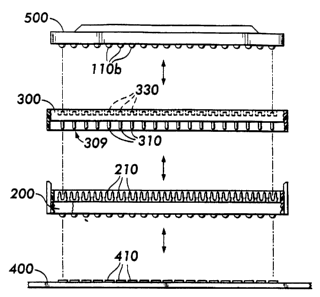
Refernng to Figs. 1 through 3, the component to connector to substrate
assembly includes a first connector half 200, such as an array connector half
having fusible
CA 02357159 2001-09-10
BERG2456 - 7 - PATENT
elements such as ball type contact portions 110a, a substrate 400, such as a
PCB, on which the
first connector half 200 is to be mounted, an electrical device 500 or other
similar component
having fusible elements such as ball type contact portions 1 l Ob, and a
second connector half
300 on which the electrical device 500 is to be mounted. The electrical device
500 may be
attached to the body of the second connector half 300 by solder reflow of the
array of ball type
contact portions 1 l Ob onto a corresponding array of contacts 309. The body
of contacts 309
have mating portions 310 and mounting regions 330. The mounting regions 330
preferably
reside within a recess 331 in the bottom of connector 300.
The second connector half 300 mates with the first connector half 200 via the
insertion of pin or blade portions 310 into receptacle contacts 210. However,
contact portions
210 and 310 may be any type of matable connector contact portions. As shown in
the
exemplary embodiment, first contact portions 210 are dual beams (Fig. 3) and
second contact
portions 310 are blades. Contact mounting regions 330, while depicted in Fig.
4 as a straight
tail, may be variously formed to provide electrical contact between contact
portions 310 and
ball type contact portions 1 l Ob. For example, contact portions 310 may
extend above the
surface of a contact mounting region 330 for connection to ball type contact
portions 1 l Ob
after reflow or the tail could be a tab bent to a portion parallel to device
500.
The first connector half 200 includes an array of fusible elements such as
ball
type contact portions 1 l0a that may be attached to substrate 400 by solder
reflow. Connector
half 200 also includes an array of dual beam contacts 210 that mate with
corresponding
contact portions 310. The substrate 400 has an array of solder pads 410
corresponding to the
array of ball type contact portions 110a. When connector half 200 is placed on
substrate 400,
an electrical connection may be made via solder reflow between the ball type
contact portions
110a and contacts 410 since in conventional applications, component 500 would
directly
mount to substrate 400.
Thus, in accordance with the present invention, the connector halves 200 and
300 may be mated together forming an electrical connection between the
component 500 and
the substrate 400. Use of this novel assembly has the added benefit that the
connector halves
CA 02357159 2001-09-10
BERG-2456 - 8 - PATENT
absorb differentials in CTEs between the component 500 and substrate 400 since
in
conventional applications, component 500 would directly mount to substrate
400.
As shown in more detail in the isolated view of Figure 3, solder ball 1 l Ob
of
electrical device S00 is adapted to attach to contact 330 of second connector
half 300 by way
of solder reflow. Solder ball 1 l0a of first connector half 200 is adapted to
be connected to the
contact region 410 of substrate 400 by way of solder reflow as well.
Subsequently, second
contact portion 310 is mated to first contact portion 210.
Typically, the mating between connector halves 200 and 300 is achieved by
inserting contact portion 310 between fingers 210a and 210b. The substantially
straight
elongated connector portion 310 pushes elongated connector portions 210a and
210b away
from one another in a direction substantially orthogonal to the mating
direction, thereby spring
biasing the connecting portions 210a and 210b against connector portion 310.
The spring
biasing and wiping action during insertion helps bolster the electrical
integrity of the electrical
connection. Contact portions 210a and 210b can have any configuration suitable
for
establishing an electrical connection. For example, they may have a curved "S"
or double
"C"shape. Moreover, portions 210a and 210b may be formed from a single piece
of contact
material, although separate pieces can be placed together.
In this fashion, CTE mismatch problems due to differences in size and material
composition between a component 500 and a substrate 400 can be avoided. The
bodies 200
and 300 of the connector provide a middle ground, in effect, to spread out any
mismatch that
may exist over a greater distance and over more pliant or flexible materials,
less prone to
mismatch problems.
Fig. 4 is an illustration of an element having an array of ball type contact
portions constructed in accordance with the present invention. As shown on a
surface of body
120, contacts 100 are formed for the reception of ball type contact portions
110. A discussion
of methods of securing a solder ball to a contact and to a PCB is contained in
International
Publication number WO 98/15989 (International Application number
PCT/LTS97/18066), the
teachings of which are hereby incorporated by reference.
CA 02357159 2001-09-10
BERG-2456 - 9 - PATENT
Fig. SA illustrates an alternate embodiment of contact portions 210. As shown,
the contact portion 210 has elongated connector portions 211 a and 211 b
electrically attached
to first connector half 200. In Fig. SA, elongated connector portions 211 a
and 21 lb have an
outwardly arced or bent shape. Portions 211a and 211b are preferably formed
from a single
piece of contact material, although separate pieces can also be placed
together.
In Fig. SB, connector portions 210a1 and 210b1 of contact portion 210 are
separate elongations with a rounded tip, and are formed from a single piece of
contact
material. Similarly, in Fig. SC, connector portions 210a2 and 210b2 of contact
portion 210
are separate elongations with a substantially pointed tip, and are formed from
the same contact
material.
Substantially straight elongated contact portion 310 pushes elongated
connector portions 210a and 210b away from one another in a direction
substantially
orthogonal to the mating direction, thereby causing wiping to occur during
insertion and
spring biasing the contact portions 210a and 210b against connector portion
310. This spring
biasing helps to bolster the electrical integrity of the electrical connection
established by the
first and second connector halves 200 and 300.
Figure 6 illustrates alternative grid an ay contact portions on device 500
that
may be used in accordance with the present invention. Thus far, ball type
contact portions
110 have been described and illustrated. However, many different types of
array type contact
portions can be used in accordance with the present invention depending on the
application for
which a component 500 is suited, depending on the materials comprising either
the substrate
400 or component 500, or depending on the type of manufacture for the
substrate 400 or
component 500. Thus, column grid array contact portions 600, ceramic ball grid
array contact
portions 610, tab ball grid array contact portions 620 and plastic ball grid
array contact
portions 630 may all be used within the spirit and scope of the present
invention.
The fusible contacts 110 on the electrical device 500 and contacts 330 on the
second array connector will preferably be a solder ball. It is noted, however,
that it may be
possible to substitute other fusible materials which have a melting
temperature less than the
melting temperature of the elements being fused together. The fusible element,
such as a
CA 02357159 2001-09-10
BERG-2456 - 10 - PATENT
solder ball, can also have a shape other than a sphere. As mentioned, examples
include
column grid arrays 600, ceramic ball grid arrays 610, tab ball grid arrays 620
and plastic ball
grid arrays 630.
When the conductive or fusible element is solder, it will preferably be an
alloy
which is in the range of about 10% Sn and 90% Pb to about 90% Sn and 10% Pb.
More
preferably the alloy will be eutectic which is 63% Sn and 37% Pb and has a
melting point of
183 °C. Typically, a "hard" solder alloy with a higher lead content
would be used for mating
materials such as ceramics. A "hard" contact will "mushroom" or deform
slightly as it
softens. A "soft" eutectic ball reflows and reforms at lower temperatures.
Other solders
known to be suitable for electronic purposes are also believed to be
acceptable for use in this
method. Such solders include, without limitation, electronically acceptable
tin-antimony, tin-
silver and lead silver alloys and indium. Before the conductive element is
positioned in a
recess, that recess is usually filled with a solder paste.
While it is believed that a solder paste or cream incorporating any
conventional
organic or inorganic solder flux may he adapted for use in this method, a so-
called "no clean"
solder paste or cream is preferred. Such solder pastes or creams would include
a solder alloy
in the form of a fine powder suspended in a suitable fluxing material. This
powder will
ordinarily be an alloy and not a mixture of constituents. The ratio of solder
to flux will
ordinarily be high and in the range of 80% - 95% by weight solder or
approximately 50% by
volume. A solder cream will be formed when the solder material is suspended in
a rosin flux.
Preferably the rosin flux will be a white rosin or a low activity rosin flux,
although for various
purposes activated or superactivated rosins may be used. A solder paste will
be formed when
a solder alloy in the form of a fine powder is suspended in an organic acid
flux or an inorganic
acid flux. Such organic acids may be selected from lactic, oleic, stearic,
phthalic, citric or
other similar acids. Such inorganic acids may be selected from hydrochloric,
hydrofluoric and
orthophosphoric acid. Cream or paste may be applied by brushing, screening, or
extruding
onto the surface which may advantageously have been gradually preheated to
ensure good
wetting.
CA 02357159 2001-09-10
BERG-2456 -11- PATENT
Heating or solder reflow is preferably conducted in a panel infra red (IR)
solder
reflow conveyor oven. The components with solder portions would then be heated
to a
temperature above the melting point of the solder within the solder paste.
While the present invention has been described in connection with the
preferred embodiments of the various figures, it is to be understood that
other similar
embodiments may be used or modifications and additions may be made to the
described
embodiment for performing the same function of the present invention without
deviating
therefrom. It will be appreciated by those of ordinary skill in the art that
the description given
herein with respect to those Figures is for exemplary purposes only and is not
intended in any
way to limit the scope of the invention.
For example, an electrical connector is described herein having a
substantially
square or rectangular mounting surface. However, the particular dimensions and
shapes of
connectors shown and described are merely for the purpose of illustration and
are not intended
to be limiting. The concepts disclosed herein have a broader application to a
much wider
variation of connector mounting surface geometries. The concepts disclosed
with reference to
this connector assembly could be employed, for example, with a connector
having a
connection mounting surface having a more elongated, irregular or radial
geometry.
Further, the first and second connector halves are described with reference to
an array of plug contact mating ends 310 on the second connector half 300
being insertable
into an array of corresponding dual-pronged receptacle mating portions 210 on
the first
connector half 200 to achieve electrical communication between the first and
second
connector halves. However, a variety of pin to receptacle implementations are
available for
use, and could be employed in the present invention to achieve electrical
communication by
inserting the first connector half into the second connector half, or vice
versa. Further, the
first connector half elongated portions 210a and 210b are interchangeable with
the second
connector half elongated portion 310 and vice versa. Therefore, the present
invention should
not be limited to any single embodiment, but rather construed in breadth and
scope in
accordance with the recitation of the appended claims.