Note: Descriptions are shown in the official language in which they were submitted.
CA 02357607 2001-09-20
REFLECTION TYPE DIFFRACTION GRATING
BACKGROUND OF THE INVENTION
The present invention relates to a spectroscopic optical
device, especially to a reflection type diffraction optical device
used widely in an optical technology field such as an optical
sensor, an information recording device, an optical measuring
device, and so on.
Diffraction gratings are used popularly as spectroscopic
optical devices or optical demultiplexing devices. Among these
diffraction gratings, a reflectiontype diffraction grating using
diffracted light as reflected light is, in most cases, configured
in such a manner that a metal film is formed as a reflection
film on a surface of a member having grooves formed periodically
so as to improve reflection efficiency of the reflection type
diffraction grating. A high-reflectance material such as A1,
Au, or the like, is used as the metal film provided on the surface
of the periodically grooved member.
If such reflection metal films are used in a state of being
exposed to an environment, weather resistance and abrasion
resistance of these reflection metal films may be insufficient.
Particularly it is known that an A1 film is inferior in oxidation
resistance. An Au film is insufficient in mechanical strength.
In order to improve durability of such a reflection metal film,
- 1 -
CA 02357607 2001-09-20
generally, the planar metal film is coated with a transparent
dielectric film or the like . It is known that oxidation resistance
particularly in the case of a reflection A1 film is improved
when a magnesium fluoride (MgF~) film is used as a protective
film of the reflection Al film. It is also known that the MgF
film has an effect in improving reflectance in a near-ultraviolet
region.
It is however known that a reflection type diffraction grating
having a groove period in a range of from 0.1 to 10 times as
large as the wavelength of incident light has its diffracted
light intensity varying in dependence on polarization of incident
light (for example, see 0 plus E, Vo1.21, No.5, p.511 (1999)).
A polarization separating device positively using this
characteristic for separating polarized light has been proposed
(for example, see Optronics, No.8, p.112 (1996)).
On the other hand, when such a diffraction optical device
is used as a demultiplexing device in the field of optical
communication or the like, it is necessary to keep the intensity
of diffracted light constant regardless of the state of
polarization of incident light. For example, in wavelength-
multiplex communication, light with a large number of wavelengths
which is transferred by one optical fiber needs to be spectrally
distributed by a diffraction grating in order to read information
of individual wavelengths. On this occasion, the state of
polarization of light emitted through the optical fiber is not
- 2 -
CA 02357607 2001-09-20
controlled. Hence, when the light is made incident on the
diffraction grating directly, the intensity of diffracted light
depends on the state of polarization. There arises a problem
that information processing of such light is made complex.
Also when a reflection type diffraction optical device is
applied to the case where light from a laser light source is
condensed and irradiates a fine roughness structure of the
diffraction optical device to read out the shape of the fine
roughness structure, sensitivity of the reflection type
diffraction optical device is lowered in accordance with the
state of polarization of the laser light source so that signal
analysis is made complex.
To control the polarization of light incident on such a
diffraction optical device, a method of inserting a polarizer,
a filter or the like in an optical system has been proposed.
In the proposed method, however, insertion loss is produced because
of the inserted device as well as the optical system is made
complex because of increase in the number of devices. There
is a problem that the intensity of light is lowered.
SUMMARY OF THE INVENTION
The present invention is devised to solve the aforementioned
problems and an object of the invention is to provide a reflection
type diffraction grating in which the intensity of reflected
light can be obtained without lowering of reflectance and
regardless of the state of polarization of incident light.
- 3 -
CA 02357607 2001-09-20
According to the present invention, there is a reflection
type diffraction grating having a groove period which is 0.1
to 10 times as large as a wavelength of incident light, a laminate
of a metal film as a first layer with reflectance not lower than
30 o and a transparent dielectric film as a second layer, the
first and second layers being laminated in order on a surface
side of the groove period.
Preferably, the metal film has a refractive index not higher
than 2.0 and an extinction coefficient not smaller than 6.0 with
respect to the wavelength of the incident light; and the dielectric
film has a refractive index in a range of from 1.30 to 1.65,
both inclusively, with respect to the wavelength of the incident
light and has an optical film thickness 0.20 to 0.80 times, both
inclusively, as large as the wavelength of the incident light.
Further preferably, the dielectric film has a refractive
index in a range of from 1.30 to 1.46, both inclusively, with
respect to the wavelength of the incident light and has an optical
film thickness 0.20 to 0.38 times, both inclusively, as large
as the wavelength of the incident light.
The above-mentioned characteristics may be realized when
the metal film is constituted by any one selected from A1 or
an alloy containing A1 as a main component, Ag or an alloy containing
Ag as a main component, Cu or an alloy containing Cu as a main
component, and Au or an al loy containing Au as a main component .
2 5 The present disclosure relates to the subj ect matter contained
- 4 -
CA 02357607 2001-09-20
in Japanese patent application No. 2000-286546 (filed on September
21, 2000), which is expressly incorporated herein by reference
in its entirety.
BRIEF DESCRIPTION OF THE DRAWINGS
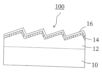
Fig. 1 is a sectional view showing the structure of a reflection
type diffraction grating according to the present invention.
Fig. 2 is a view showing an optical system for evaluating
polarization dependence of diffraction efficiency.
DESCRIPTION OF THE PREFERRED EMBODIMENT
The present invention will be described below on the basis
of an embodiment thereof. First, simulation was performed by
use of a method called matrix method in order to find out a film
configuration for achieving the object of the present invention.
This method has been described in detail in the reading "Optical
Thin Film" (The Nikkan Kogyo Shinbun Ltd. ) written by H.A. Macleod.
From this simulation, the inventors of this application
have found that a laminate structure in which a metal film and
a transparent dielectric film are provided on a flat substrate
makes it possible to achieve an optical reflecting mirror free
from polarization even in the case where light is made incident
obliquely.
From results of this simulation, it has been concluded that
a material with an extinction coefficient (imaginary part of
a complex index of refraction) k which is not smaller than 6.0
is preferably used as the metal film in order to make reflectance
- 5 -
CA 02357607 2001-09-20
high. Incidentally, in a general metal, k is equal to or smaller
than about 20. From another point of view, a material with a
refractive index (real part of the complex index of refraction)
n which is not higher than 2.0 is preferably used as the metal
film. In a general metal, n is equal to or larger than about
0.2. Examples of the metal material satisfying such
characteristics are A1, Ag, Au, and Cu. Any one of these metal
materials may be used as a single-element metal or an alloy
containing any one of these metal materials as a main component
may be used.
It has been also found that the transparent dielectric film
needs to have a refractive index in a range of from 1.30 to 1.65,
both inclusively, with respect to the wavelength of incident
light and needs to have an optical film thickness in a range
of from 0.201 to 0.801, both inclusively, when 1~ is the wavelength
of incident light . Further, it is preferable that the transparent
dielectric film has a refractive index in a range of from 1.30
to 1.46, both inclusively, with respect to the wavelength of
incident light and has an optical film thickness of from 0.201
to 0.38?, both inclusively. Examples of the material for the
transparent dielectric film satisfying such characteristic may
include: magnesium fluoride, si7_icon dioxide, titanium dioxide
and aluminum oxide which will be described in Examples; and calcium
fluoride, aluminumfluoride, yttriumfluoride, ytterbiumfluoride,
silicon monoxide, and so on. Especially, a fluorine compound
- 6 -
CA 02357607 2001-09-20
such as magnesium fluoride, calcium fluoride or the like is
preferably used because the compound does not oxidize a surface
of the metal film when a film of the compound is formed on the
metal film.
The material for a diffraction grating substrate is not
particularly limited. Also the method of forming a surface
fine-roughness groove structure serving as a diffraction grating
is not particularly limited.
The method of forming the metal film and the transparent
dielectric film in the present invention is not particularly
limited. For example, each of the films may be formed by use
of a suitable method such as a vacuum evaporation film-forming
method, a sputtering film-forming method, a sol-gel film-forming
method, a chemical vapor-phase deposition method (CVD) , a vacuum
evaporation film-forming method using plasma called ion plating,
or the like.
Incidentally, when adhesion between an Au film used as the
metal film and the substrate is insufficient, for example, a
Cr film or the like may be used as an intermediate layer between
the substrate and the metal film in accordance with the necessity.
That is, the metal film need not be limited to a single-layer
film.
[Example 1]
A fine roughness structure of a diffraction grating according
to the present invention was produced by the following method.
CA 02357607 2001-09-20
First, a sol solution containing a liquid hydrolysate of
methyltriethoxysilane as a main component was applied onto a
glass substrate 10 shown in Fig. 1 by spin coating. This
sol-solution-appliedsubstratel0 waspress-molded whilea brazed
replica diffraction grating (900 /mm) which was subjected to
mold release treatment and which was available on the market
was used as a stamping mold. Then, mold release treatment and
baking were performed to thereby obtain a fine roughness structure
12 serving as a diffraction grating. The depth of each of the
roughness grooves was about 1 um. A1 was vacuum-deposited on
a surface of the fine roughness structure to thereby form a metal
film 14 with a thickness of 100 nm. The reflectance of the A1
film was not lower than 90 o with respect to non-polarized light.
Silicon dioxide (Si02) and titanium dioxide (Ti02) were
vacuum-deposited successively on the A1 film to thereby form
a dielectric film 16 constituted by two layers 280 nm and 170
nm thick. Thus, a reflection type diffraction grating 100
according to the present invention was obtained.
The diffraction efficiency of the diffraction grating was
evaluated, by use of an optical system shown in Fig. 2, as follows.
Light 50 emitted froma laser light source 20 of a 1550 nm-wavelength
region through an optical fiber 22 was collimated by a collimator
lens 24. The collimated light 52 was made to pass through a
quarter-wave plate 26 to thereby generate linearly polarized
light 54. Then, the light 54 was made to pass through a half-wave
_ g _
CA 02357607 2001-09-20
plate 28 the rotational angle of which has been adjusted to thereby
control the state of polarization of the light. Thus, the
diffraction grating 100 was irradiated with the light. Primary
diffracted light in each of TE-polarized light and TM-polarized
light obtained thus was condensed by a lens 30 so as to be incident
on a light-receiving device 32. The quantity of the diffracted
light was estimated on the basis of a generated current and compared
with the quantityof reflected light in the case of anAl single-layer
filmtothereby calculatediffraction efficiencyofthe diffraction
grating 100 with respect to each of the TE-polarized light and
the TM-polarized light.
As a result, the diffraction efficiency of the diffraction
grating having an Al single layer was 25.9 % with respect to
the TE-polarized light and 77. 1 % with respect to the TM-polarized
lightwhereasthe diffractionefficiencyofthe diffraction grating
having the dielectric film formed on the Al layer was 45.1
with respect to the TE-polarized light and 74.5 o with respect
to the TM-polarized light. The later diffraction grating was
possible to improve polarization dependence. Further, increase
of stray light due to the dielectric film formation was evaluated.
No change of stray light was observed.
[Example 2)
A1 and magnesium fluoride (MgF2) were deposited on a
holographic replica diffraction grating (900 /mm, provided with
a reflection A1 film formed thereon) available on the market
_ g _
CA 02357607 2001-09-20
to thereby form two layers 100 nm and 250 nm thick respectively.
That is, this Example has two metal films (an Al film originally
provided on the holographic replica diffraction grating, and
another A1 deposited on the holographic replica diffraction
grating). The diffraction efficiency of the thus produced
diffraction grating with respect to the wavelength of 1550 nm
was measured in the same manner as that in Example 1 . As a result,
the diffraction efficiency of the diffraction grating having
an A1 single layer was 32.8 o with respect to the TE-polarized
light and 82.5 % with respect to the TM-polarized light whereas
the diffraction efficiency of the diffraction grating having
the dielectric film formed on the A1 layer was 41. 9 % with respect
to the TE-polarized light and 54 . 9 o with respect to the TM-polarized
light. That is, the later diffraction grating was slightly lowered
in reflectance but its polarization dependence was improved more
greatly. Further, increase of stray light due to the dielectric
film formation was evaluated. No change of stray light was
observed.
[Comparative Example 1]
The diffraction efficiency of a brazed replica diffraction
grating (provided with a reflection Al film formed thereon)
available on the market was measured with respect to the wavelength
of 1550 nm. As a result, the diffraction efficiency was 30.6 0
with respect to the TE-polarized light and 58.7 ~ with respect
to the TM-polarized light. The diffraction grating was low in
- 10 -
CA 02357607 2001-09-20
reflectance and large in polarization dependence.
[Comparative Example 2]
An Au thin film 100 nm thick was sputtered onto the holographic
replica diffraction grating (900 /mm, provided with a reflection
A1 film formed thereon) available on the market. The diffraction
efficiency of the thus produced diffraction grating was measured
with respect to the wavelength of 1550 nm. As a result, the
diffraction efficiency was 28.0 o with respect to the TE-polarized
light and 65 . 5 o with respect to the TM-polarized light . Further,
increase of stray light due to the Au thin film formation was
evaluated. As a result, there was no change of stray light observed.
However, the diffraction grating was low in reflectance and
large in polarization dependence.
[Effect of the Invention]
According to the present invention, there can be achieved
a reflection type diffraction grating which is small in the change
of diffraction efficiency with respect to polarized light and
high in reflectance. Hence, a filter or the like which is required
to be inserted in an optical system to lower polarization dependence
in the background art becomes needless, so that spectral
sensitivity can be made high as well as the optical system can
be made simple.
- 11 -