Note: Descriptions are shown in the official language in which they were submitted.
CA 02357689 2001-09-18
SPECIFICATION
TITLE OF THE INVENTION
OPTICAL COMMUNICATION SYSTEM AND OPTICAL RECEIVER
BACKGROUND OF THE INVENTION
(1) Field of the Invention
The present invention relates to an optical
communication system and an optical receiver.
(2) Description of Related Art
In the recent years, the employment of a large-scale
integrated circuit (LSI) has permitted an error correction
code to be used as a transmission code. At present, an
LSI capable of correcting and reducing an error rate of
2 x 10⁻⁴ up to an error rate of approximately 10-15 has been
put to practical use. And not only that, an LSI provided
with an error correction code for making correction from
1 x 10⁻² to 10-15 has been in development.
Naturally, in the case of the employment of such a
high correction capability code, an optical receiver would
be required to operate normally in poor S/N conditions
causing an error rate of 1 x 10⁻².
So far, the optical receiver has conducted an operation
to make up an input to an identification unit to a constant
amplitude for normal identification. As this approach,
there has been employed a structural example in which a
peak value of an equalized waveform signal after
amplification is detected to give feedback (see FIG. 6)
1
CA 02357689 2001-09-18
or a structural example in which an optical output power
is made constant by an optical amplifier (see FIG. 7).
In FIG. 6, reference numeral 1 represents a
light-receiving device (PD: PhotoDiode), numeral 2
represents a gain variable type preamplifier [AGC
(Automatic Gain Controlled) amplifier], numeral 3
represents a low-pass filter (LPF), numeral 4 designates
a band-pass filter (BPF), numeral 5 designates a
differential amplifier, numeral 6 designates a flip-flop
circuit (FF), numeral 7 depicts a peak value detecting
circuit, numeral 8 depicts a limiter amplifier, numeral
9 depicts a signal identifying section, numeral 10 denotes
a buffer amplifier, and numeral 18 denotes a clock extracting
circuit.
In the optical receiver shown in FIG. 6, a PD 1
comprising a PIN photodiode or an avalanche photodiode
receives light from an optical transmission line, and the
preamplif ier 2 amplif ies the output of the PD 1. The output
of the preamplifier 2 is inputted to the low-pass filter
2 and further to band-pass filter 4. The low-pass filter
3 is a filter having 3-dB down band corresponding to 0.7
to 0.8 of the bit rate of a received signal. The output
of the low-pass filter 3 is inputted to the differential
amplifier 5 and further to the peak value detecting circuit
7.
The peak value detecting circuit 7 is for detecting
a peak value of a signal (received data signal) inputted
2
CA 02357689 2001-09-18
to the differential amplifier 5 of the signal identifying
section 9 and adjusting the gain of the preamplifier 2 to
make constant the signal level inputted to the signal
identifying section 9. The differential amplifier 5 of
the signal identifying section 9 is for shaping a signal
waveform in its amplitude direction by applying a value
minimizing the error rate as a reference voltage Vref.
The band-pass filter 4 of the clock extracting circuit
18 is a filter for clock extraction, which detects a frequency
(clock component) corresponding to the bit rate of a data
signal. In this connection, the clock extracting circuit
18 shown in FIG. 6 has an arrangement for when the signal
to be sent from the optical transmission line is an RZ (Return
to Zero) signal. In the case of an NRZ (Non-Return to Zero ),
since a clock component does not exist in the signal spectrum
unlike the RZ signal, there is a need to place a
differentiating circuit for detecting an edge of a signal
and a rectifying circuit for rectifying the output of the
differentiating circuit in the former stage of the band-pass
filter 4 to generate a clock for signal identification.
The output of the band-pass filter 4 is inputted to
the limiter amplifier 8, and the limiter amplifier 8 cuts
off both a peak level and bottom level of the output of
the band-pass filter 4 and amplifies the received signal
so that its upper limit and its lower limit assume
predetermined values, respectively, f or clock production.
The clock thus shaped in the limiter amplifier 8 is inputted
3
CA 02357689 2001-09-18
to the flip-flop circuit 6 of the signal identifying section
9. The flip-flop circuit 6 punches the output of the
differential amplifier 5 with the output of the limiter
amplifier 8 for outputting data subjected to signal
identification. The buffer amplifier 10 is for setting
up the circuit isolation.
On the other hand, in a configuration shown in FIG.
7, an optical amplifier 11, such as an EDF (Erbium Doped
Fiber) amplifier, is provided at the final stage of an optical
transmission line. In the FIG. 7 configuration, the same
parts as those in FIG. 6 are marked with the same reference
numerals. This optical amplifier 11 is designed to
implement constant output control so that the signal power
to be inputted to the PD 1 is made constant at all times.
Accordingly, a preamplifier 2' at the latter stage
is required to perform simple amplification only, and this
eliminates the need for the feedback control based on the
received signal peak value detection in the FIG. 6
configuration.
Meanwhile, the received waveform in the
above-mentioned optical receiver varies, for example, as
shown in FIGs. 8A to 8C according to optical S/N. FIG.
8A shows a received waveform (eye pattern) in a case in
which the S/N is at 8 dB (error rate = 1 x 10⁻¹), FIG. 8B
shows a received waveform in a case in which the S/N is
at 17. 5 dB (error rate = 1 x 10"4 ), and FIG. 8C shows a received
4
CA 02357689 2001-09-18
waveform in a case in which the S/N is at 21.5 dB (error
rate = 1 x 10⁻⁹ ) .
For example, in the poor optical S/N condition shown
in FIG. 8A, in an optical receiver with the configuration
shown in FIG. 6, the peak value detecting circuit 7 detects
a peak value of a noise instead of a peak value of the intended
received signal (data signal), and the amplitude of the
received signal (data signal) inputted to the signal
identifying section 9 becomes lower than the proper
amplitude. For this reason, the signal identification
indeterminate factors increase so that the actual error
rate is impaired as compared with the error rate based on
the optical S/N. Moreover, since the amplitude inputted
to the clock extracting circuit 18 decreases, it tends to
be out of the dynamic range of the clock extracting circuit
18.
In the poorer optical S/N condition, the ASE (Amplified
Spontaneous Emission) light increases, which decreases the
optical signal component with respect to the entire light.
With this fact, in the case of the FIG. 7 configuration
of the optical receiver which implements the constant output
control on the entire light in the optical amplifier 11,
similarly, the amplitude of the received signal to be
inputted to the signal identifying section 9 becomes lower
and the amplitude to be inputted to the clock extracting
circuit 18 also becomes lower, which creates the same problem
as that of the optical receiver with the configuration shown
5
CA 02357689 2008-10-17
29385-2
in FIG. 6.
In addition, although the error correction code is
capable of correcting an error of a data signal, it is
helpless against a case in which a clock signal falls into a
malfunctioning condition. Although simple clock extracting
circuits using a PLL circuit have frequently been put to
use, if the optical S/N is in a poor condition, since a
large noise is introduced into a phase comparator
constituting the PLL circuit, the phase jump of the clock
occurs to cause the out-of-synchronization, thereby
producing huge burst errors.
For these reasons, the conventional optical
receivers shown in FIGs. 6 and 7 do not function normally
when a received signal is in a low S/N condition.
SUMMARY OF THE INVENTION
The present invention has been developed with a
view to eliminating these problems, and it is therefore an
object of some embodiments of the invention to provide an
optical communication system and an optical receiver,
capable of functioning excellently even when a received
signal is in a poor S/N condition.
For this purpose, according to an aspect of the
present invention, when a signal amplitude is controlled on
an optical receiver side, amplitude information on a
specific spectrum (frequency component) involved in a data
signal is detected instead of extraction of a peak of the
data signal to implement the amplitude control on the data
signal on the basis of the amplitude information, which
allows the data signal to be amplitude-controlled without
being affected by S/N.
6
CA 02357689 2008-10-17
j 29385-2
That is, in accordance with another aspect of the
present invention, there is provided an optical
communication system comprising an optical transmitter for
transmitting a data signal developing a specific spectrum at
a predetermined frequency, and an optical receiver for
detecting the amplitude information on the spectrum included
in the data signal transmitted from the optical transmitter
to control the data signal to a constant amplitude on the
basis of the amplitude information.
Thus, according to some embodiments of the present
invention, a data signal producing a specific spectrum is
transmitted at a predetermined frequency by a transmission
side while the spectrum is detected on the receive side to
implement control to keep the amplitude of the received data
signal constant; therefore, it is possible to realize an
optical communication system and an optical receiver capable
of functioning excellently even if the optical S/N is in an
extremely poor condition.
In this configuration, it is preferable that the
optical receiver is composed of a signal identifying section
for identifying the data signal, amplitude adjusting means
capable of adjusting an amplitude of the data signal
inputted to the signal identifying section, and control
means for detecting the amplitude information on the
spectrum from the data signal to control the amplitude
adjusting means on the basis of the amplitude information so
that the amplitude of the data signal inputted to the signal
identifying section becomes constant.
In addition, it is also appropriate in some
embodiments that the amplitude adjusting means is
constructed as an optical amplifier capable of, when
receiving the data signal in the form of an optical signal,
7
CA 02357689 2008-10-17
29385-2
adjusting the amplification degree of the optical signal,
while the control means is designed to control the amplitude
of the data signal inputted to the signal identifying
section by controlling the amplification degree of the
optical amplifier.
Still additionally, it is also appropriate in some
embodiments that, for developing the spectrum at the
predetermined frequency, an RZ (Return to Zero) signal is
used as the data signal, or that a transmission optical
signal is amplitude-modulated.
Moreover, it is also appropriate in some
embodiments that the control means of the optical receiver
is composed of a first clock extracting circuit including a
first filter for extracting a frequency component of the
spectrum from the data signal and a clock generating section
for shaping the waveform of the output of the first filter
to generate a clock signal for identification of the data
signal in the signal identifying section, and a first
amplitude detecting circuit for detecting amplitude
information on the predetermined frequency to output a
signal corresponding to the amplitude information as a
control signal for the amplitude adjusting means.
Still moreover, it is also appropriate in some
embodiments that the control means is composed of a second
filter for extracting the frequency component of the
spectrum from the data signal and a second amplitude
detecting circuit for detecting amplitude information on the
frequency component of the spectrum extracted by the second
filter to output a signal corresponding to the amplitude
information as a control signal for the amplitude adjusting
means.
8
CA 02357689 2008-10-17
29385-2
In this case, it is also appropriate in some
embodiments that the optical receiver further comprises a
differentiating/rectification circuit composed of a
differentiating circuit for detecting an edge of the data
signal and a rectifying circuit for rectifying the output of
the differentiating circuit, and a second clock extracting
circuit including a third filter for extracting a clock
signal component for identification of the data signal in
the signal identifying section from the output of the
differentiating/rectifying circuit.
In this case, preferably, the Q valves of the
first filter and the third filter are set at 300 or more.
In accordance with still another aspect of the
present invention, there is provided an optical
communication system comprising: an optical transmitter
arranged to transmit a data signal including a constant
amplitude line spectrum, at a predetermined frequency; an
optical receiver arranged to receive said data signal and to
detect amplitude information on said line spectrum included
in said data signal, the receiver comprising a first filter
arranged to extract a frequency component of said line
spectrum from the received data signal and an amplitude
detecting circuit arranged to detect amplitude information
on said frequency component and to output a signal
corresponding to said amplitude information, the optical
receiver being further arranged to control the amplitude of
the received data signal on the basis of said amplitude
information.
In accordance with yet another aspect of the
present invention, there is provided an optical receiver for
receiving a data signal transmitted from an optical
9
CA 02357689 2008-10-17
29385-2
transmitter which is arranged to transmit a data signal
including a constant amplitude line spectrum at a
predetermined frequency, comprising: a signal identifying
section arranged to make a signal identification on the
received data signal; and amplitude adjusting means arranged
to adjust an amplitude of the received data signal to be
inputted to said signal identifying section, characterized
in comprising: control means arranged to detect amplitude
information on said line spectrum included in the received
data signal, the control means comprising a first filter
arranged to extract a frequency component of said line
spectrum from the received data signal and an amplitude
detecting circuit arranged to detect amplitude information
of said frequency component and to output a signal
corresponding to said amplitude information, the control
means being further arranged to control said amplitude
adjusting means on the basis of said amplitude information
so that said amplitude of the received data signal to be
inputted to said signal identifying section is controlled.
BRIEF DESCRIPTION OF THE DRAWINGS
FIG. 1 is a block diagram showing a configuration
of an essential part of an optical communication
(transmission) system according to a first embodiment of
9a
CA 02357689 2001-09-18
the present invention;
FIG. 2 is a block diagram showing a concrete feasible
example of the optical receiver shown in FIG. 1;
FIG. 3 is a block diagram showing a modification of
the first embodiment;
FIG. 4 is a block diagram showing a configuration of
an essential part of an optical communication
(transmission) system according to a second embodiment of
the present invention;
FIG. 5A is an illustration of an example of a frequency
spectrum of an RZ signal;
FIGs. 5B and 5C are illustrations of frequency
spectrums of NRZ signals;
FIG. 6 is a block diagram showing an optical receiver
with a conventional configuration;
FIG. 7 is a block diagram showing an optical receiver
with another conventional configuration; and
FIGs. 8A to 8C are illustrations of received waveforms
(eye patterns) appearing according to optical S/N.
DESCRIPTION OF THE PREFERRED EMBODIMENTS
Embodiments of the present invention will be described
hereinbelow with reference to the drawings.
(A) Description of First Embodiment
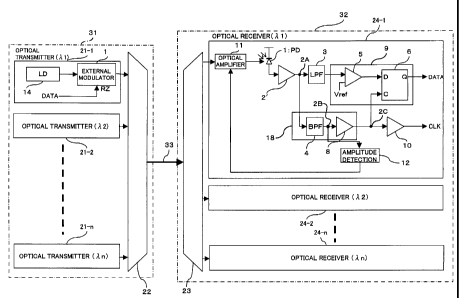
FIG. 1 is a block diagram showing a configuration of
an essential part of an optical communication
(transmission) system according to a first embodiment of
CA 02357689 2001-09-18
the present invention. In FIG. 1, this optical transmission
system is made up of an optical transmitting apparatus 31
including a plurality of optical transmitters 21-1 to 21-n
[ n corresponds to the number of wavelengths ( channels ) equal
to or more than two] and a wavelength multiplexing section
22, an optical receiving apparatus 32 including a wavelength
demultiplexing section 23 and a plurality of optical
receivers 24-1 to 24-n, and an optical transmission line
33 using an optical fiber [for example, Non-zero-DSF
(Dispersion Shifted Fiber)].
Although the internal configuration of each of the
optical transmitters 21-2 to 21-n is omitted from the
illustration, it is the same as the internal configuration
of the optical transmitter 21-1. Similarly, each of the
optical receivers 24-2 to 24-n has the same internal
configuration as that of the optical receiver 24-1. In
addition, in FIG. 1, the parts marked with the same reference
numerals as those in FIGs. 6 and 7 are the same as or similar
to those mentioned above with reference to FIGs. 6 and 7.
In the optical transmitting apparatus 31, each of the
optical transmitters 21-i ( i= 1 to n) is for generating
and transmitting an optical signal with a predetermined
wavelength ki, and for example, the essential part thereof
is composed of a laser diode (LD) 14 serving as a light
source for emitting light with a predetermined wavelength
and an external modulator 15 such as a Mach-Zehnder type
modulator as shown in FIG. 1.
11
CA 02357689 2001-09-18
The problem of the conventional optical receivers
mentioned above with reference to FIGs. 6 and 7 originates
from that a poor-S/N signal as shown in FIG. 8A is directly
used for the detection of a signal component in a case in
which regeneration of a received signal is made through
the use of an error correction code for correction from
a 1 x 10⁻² error rate to a 10-15 error rate. For eliminating
this, there is a need to previously transmit a signal which
is unaffected by a noise and subjected to attenuation by
the optical transmission line 33 in proportion to a
transmitted signal component.
Therefore, in this embodiment, an RZ (Return to Zero)
in which the mark rate for the scrambler processing is set
at 1/2 is used as the data signal to be inputted to the
aforesaid external modulator 15. As FIG. 5A shows, the
RZ signal has a constant quantity of line spectrum fb
corresponding to a data signal level at a frequency
developing an fb code transmission rate, and this line
spectrum fb attenuates in conjunction with the attenuation
of a received signal forming transmitted data, which
satisfies the foregoing conditions. Accordingly, if the
amplitude of this line spectrum fb is detected on the
reception side to control the amplitude of the received
signal as will be mentioned later, then it is possible to
realize the amplitude control of a signal unaffected by
a noise.
The wavelength multiplexing section 22 of the optical
12
CA 02357689 2001-09-18
transmitting apparatus 31 is for wavelength-multiplexing
the optical signals from the aforesaid optical transmitters
21-i to output a wavelength-multiplexed optical signal (WDM
signal) to the optical transmission line 33.
On the other hand, in the optical receiving apparatus
32, the wavelength demultiplexing section 23 is for
demultiplexing a WDM signal from the optical transmission
line 33 according to wavelength ki into optical signals.
Each of the optical receivers 24-i is for receiving the
corresponding one of the optical signals obtained by the
demultiplexing according to wavelength ki in the wavelength
demultiplexing section 23. In this embodiment, a band-pass
filter (first filter) 4 of a clock extracting circuit 18
extracts (detects) the aforesaid line spectrum fb (clock
component) from the output (data signal) of a preamplifier
2', and an amplitude detecting circuit (first amplitude
detecting circuit) 12 detects amplitude information (peak
value) on the line spectrum fb, with an output level ( gain )
of an optical amplifier 11 serving as an amplitude adjusting
means being feedback-controlled on the basis of a result
of the detection.
That is, in this embodiment, the clock extracting
circuit 18 and the amplitude detecting circuit 12 function
as a control means to control the output level of the optical
amplifier 11 on the basis of the amplitude of the line
spectrum fb extracted by the band-pass filter 4 to keep
13
CA 02357689 2001-09-18
constant the amplitude of the data signal to be inputted
to the signal identifying section 9.
A description will be given hereinbelow of an operation
of the optical transmission system thus arranged according
to this embodiment. First of all, in the optical
transmitting apparatus 31 (which sometimes will be referred
to hereinafter as a "transmission side 31"), each of the
optical transmitters 21-i modulates light (wavelength ki)
from an LD 14 with an RZ signal (data signal) in an external
modulator 15. This RZ signal is a signal
scrambler-processed so that the mark rate is set at 1/2.
Incidentally, as the data signal modulation method,
it is also acceptable to employ VSB (Vertical Side-Band
Modulation), CS-RZ (Carrier Suppressed Return to Zero)
modulation, or the like. The CS-RZ modulation method is
a technique for inverting (antiphase) an optical carrier
phase between adjacent pulses of an optical signal pulse
string, and is capable of suppressing a high-level optical
carrier frequency component appearing in an RZ signal or
NRZ (Non-Return-to-Zero) signal and of generating a pulse
signal in which the occupied wavelength band is suppressed
to approximately 1/2. Accordingly, employment of these
modulation methods enables increasing the number of
wavelengths to be multiplexed.
The optical signals modulated in the external
modulators 15 of the optical transmitters 21-i as mentioned
above are wavelength-multiplexed in the wavelength
14
CA 02357689 2001-09-18
multiplexing section 22 and outputted as a WDM signal to
the optical transmission line 23 to be transmitted to the
optical receiving apparatus 32.
In the optical receiving apparatus 32 (which sometimes
will be referred to hereinafter as a "reception side 32" ),
the wavelength demultiplexing section 23 demultiplexes the
WDM signal from the optical transmission line 33 according
to wavelength Xi into optical signals which in turn, are
inputted to the corresponding optical receivers 24-i. In
each of the optical receivers 24-i, a light-receiving device
1 receives the inputted optical signal and converts it into
an electric signal which in turn, is inputted to a
preamplifier 2'.
The preamplifier 2' amplifiers the electric signal
from the light-receiving device 1. The output signal of
the preamplifier 2' is inputted to a low-pass filter 3 and
further to the band-pass filter 4 of the clock extracting
circuit 18. In the clock extracting circuit 18, the
band-pass filter 4 fetches the aforesaid line spectrum fb,
thereby removing noise components.
The output (line spectrum f b) of the band-pass filter
4 is inputted to a limiter amplifier 8. The limiter
amplifier 8 cuts off the peak level and bottom level of
the output of the band-pass filter 4 and amplifies the
received signal so that its upper and lower limits assume
predetermined values, thereby generating a clock signal.
That is, the limiter amplifier 8 functions as a clock
CA 02357689 2001-09-18
generating section to shape the waveform of the output of
the band-pass filter 4 for generating a clock for the signal
identifying section 9.
The clock signal thus formed in the limiter amplifier
8 is inputted to a flip-flop circuit 6 of the signal
identifying section 9. The flip-flop circuit 6 punches
the output of a differential amplifier 5 with the output
of the limiter amplifier 8 to output data undergoing signal
identification.
On the other hand, the amplitude detecting circuit
12 detects the amplitude value of the clock signal [line
spectrum fb (predetermined frequency)] from the output
signal of the band-pass filter 4 to output a signal
corresponding to that amplitude value as a control signal
for controlling the output level (amplification degree)
of the optical amplifier 11. To this end, the amplitude
of the received data signal to be inputted to the signal
identifying section 9 is maintainable constant irrespective
of noise, and the optical receivers 24-i work well even
if the received signal is in a poor S/N condition.
(Al) Example of Realization of Optical Receivers 24-i
FIG. 2 is an illustration of an example of realization
of the above-mentioned optical receiver 24-i. In the
optical receiver 24-i shown in FIG. 2, numeral 41 designates
a an optical amplifier module, numeral 42 designates an
OE module (in this case, the operating frequency is set
at 12.021494 GHz), numeral 43 denotes a CDET (Clock
16
CA 02357689 2001-09-18
DETection) module, numeral 44 denotes a VCO (Voltage
Controlled Oscillator) module, numeral 45 signifies an
optical variable attenuator for adjusting the optical input
level to the OE module 42. The attenuation degree of this
optical variable attenuator 45 is fixed in operation. In
FIG. 2, the same reference numerals as those in FIG. 1
represent the parts corresponding to those mentioned above
with reference to FIG. 1.
That is, the optical amplifier module 41 includes an
EDF (Erbium Doped Fiber) amplifier (which sometimes will
be referred to hereinafter as an "EDF 11") as the aforesaid
optical amplifier 11. In the optical amplifier module 41,
numeral 51 depicts an optical coupler which is for fetching
a portion of inputted light to output it to a monitor PD
54 and further for inputting excitation light from an
excitation laser/monitor PD module 65 to the EDF 11, and
numeral 52 depicts an optical monitor circuit having a PD
to monitor the optical output level of the EDF 11.
In addition, numeral 53 represents an optical coupler
for providing a portion (monitor light) of the output light
of the EDF 11 to the external. This optical coupler 53
is omissible if the external monitoring is unnecessary.
Numeral 54 represents a monitor PD for receiving the input
light (monitor light) from the optical coupler 51 to convert
it into an electric signal, with the output of this monitor
PD 54 being sent through monitor circuits 55, 56 and a
comparator 57 to the external to be used as a monitor output
17
CA 02357689 2001-09-18
and an alarm output (in a case in which no input light exists)
with respect to the optical input level.
Still additionally, numeral 58 indicates a narrow-band
amplifier which is for receiving a clock signal in an
intermediate f requency (IF) band acquired in the CDET module
43 to remove undesired components such as noise components
and further for amplifying this clock signal up to an
appropriate level. As mentioned above, the amplitude value
of the clock signal is detected from the output thereof
in the amplitude (peak) detecting circuit 12.
Moreover, numerals 59 to 61 indicate differential
amplifiers (operational amplifiers). As input, the
operational amplifier 59 receives a voltage value
(threshold voltage) set by a voltage setting circuit 66'
and the output (voltage signal corresponding to the optical
output level of the EDF 11) of the optical monitor circuit
52, the operational amplifier 60 receives the threshold
voltage and the output (voltage signal corresponding to
the excitation light level) of the excitation laser/monitor
PD module 65, and the operational amplifier 61 receives
the threshold voltage and the output of the amplitude
detecting circuit 12.
Still moreover, numerals 59a, 60a and 61a denote
(switching) diodes each of which is made to take an H
(conducting) state when the output voltage of the
corresponding operational amplifier 59, 60 or 61 exceeds
a predetermined voltage value. Concretely, the diode 61a
18
CA 02357689 2001-09-18
takes an H state when the output voltage of the operational
amplifier 61 is in an operating range of the excitation
laser/monitor PD module 65, while each of the diodes 59a
and 59b enters an H state when the output voltage of the
corresponding operational amplifier 59 or 60 is out of the
operating range of the excitation laser/monitor PD module
65.
Accordingly, for example, in a case in which the optical
output level is too high (there is a possibility that the
PD 1 breaks down), or in a case in which the excitation
light output power of the excitation laser/monitor PD module
65 is too high (abnormality such as disconnection exists
in an optical transmission line 51a to the optical coupler
51), the output of the operational amplifier 59 or 60 comes
into effect to stop the operation of the excitation
laser/monitor PD module 65, and in the normal condition
other than these cases, the output of the operational
amplifier 61 (i. e., the output of the peak detecting circuit
12) comes into effect and the excitation light output power
is adjusted in accordance with the voltage value thereof
so that the optical output level of a data signal component
from the EDF 11 is made constant as mentioned above.
That is, the operational amplifier 59, the diode 59a,
the operational amplifier 60 and the diode 60a function
as a protecting circuit for stopping the excitation light
output upon the occurrence of abnormality, for example,
when the optical output level of the EDF 11 is too high
19
CA 02357689 2001-09-18
or when the excitation light output power to the EDF 11
is too high. Incidentally, in this example, although the
effective excitation light control signal is changed by
the setting of the diodes 59a, 60a and 61a, a similar
operation is also realizable by changing the threshold
voltage to be given from a voltage setting circuit 66' to
the operational amplifiers 59 to 61.
Yet moreover, numeral 62 represents an amplifier for
amplifying the outputs (excitation light control signal)
of the aforesaid diodes 59a, 60a and 61a up to an appropriate
level, numeral 63 represents a low-pass filter for removing
undesired (noise) components such as harmonic from the
excitation light control signal, and numeral 64 represents
a voltage/current (V/I) converting circuit for converting
the output (voltage signal) of the low-pass filter 63 into
a current signal corresponding to the voltage value thereof .
The reason for such voltage/current conversion is that the
operation of the excitation laser/monitor PD module 65
depends on a current signal.
Furthermore, in the OE module 42, numeral 66 designates
a PD-PRE module including the PD 1 and an amplifier 661
for amplifying the output (data signal) of the PD 1. Numeral
67 designates an amplification module including an
amplifier 671 for amplifying the output of the PD-PRE module
66. Numeral 68 designates a resistance divider module
including an amplifier 681 for amplifying the output of
the amplification module 67. The amplifiers 661, 671 and
CA 02357689 2001-09-18
681 function as the preamplifier 2' shown in FIG. 1.
Numeral 69 denotes a resistance divider module
including a variable attenuator (ATT) 691 capable of
adjusting the attenuation degree of one output of the
resistance divider module (which will hereinafter be
referred to simply as a "divider" ) 68 and the low-pass filter
3. This resistance divider module 69 forms a branch point
2A shown in FIG. 1. Numeral 70 denotes an amplification
module including an amplifier 701 for amplifying a branch
signal from the divider 68 to compensate for the gain thereof ,
with the output thereof being inputted to the band-pass
filter 4. This amplification module 70 also serves as a
means to preventing a signal from being reflected from the
band-pass filter 4 side to the divider 68.
Numeral 71 indicates a divider module including a
linear amplifier 89 and a clock divider 711, with the clock
divider 711 establishing a branch point 2B shown in FIG.1.
Numeral 72 indicates a clock phase adjusting module capable
of adjusting (rotating 360 ) the phase of one output (clock)
of the divider module 71. The phase adjustment in this
clock phase adjusting module 72 is under control of a control
circuit 72a.
Numera173signifiesan amplification module including
an amplifier 731 for amplifying the output (clock) of the
clock phase adjusting module 72, and numeral 74 signifies
an isolator, with the other output (clock) of the divider
71 being fed through the isolator 74 to a mixer module 82
21
CA 02357689 2001-09-18
(multiplier 821) in the CDET module 43.
Numeral 10' designates a comparator module including
a clock comparator 101, with one output of this clock
comparator 101 being given to a clock terminal (C) of the
flip-flop circuit 6 and the other output (inverting output)
thereof being supplied as a clock for a signal processing
circuit (not shown) at the latter stage. That is, this
module 10' functions as both a branch point 2C shown in
FIG. 1 and the aforesaid limiter amplifier 8.
In addition, in FIG. 2, a reference voltage Vref for
the differential amplifier 5 shown in FIG. 1 is fed from
the control circuit 6a to the flip-flop circuit 6. That
is, in this case, the flip-flop circuit 6 also functions
as the above-mentioned differential amplifier 5.
Furthermore, in the CDET module 43, numeral 75
represents a divider module including an amplifier 751 and
a clock divider 752. The output (oscillation frequency
= 12 . 001495 GHz) of aVCO 441 in the VCO module 44 is amplified
by the amplifier 751, and then fed through the clock divider
752 to the mixer module 82 side and further to prescalers
76, 77 sides. The branch clock to the latter side is divided
down to 1/8 and 1/256 in prescalers 76 and 77.
Numeral 78 designates a band amplifier for
band-amplifying the output (clock after the dividing) of
the prescaler 77, and numeral 78' designates an amplifier
for amplifying the output of this band amplifier 78.
Moreover, numeral 85 designates an oscillator [OSC
22
CA 02357689 2001-09-18
(oscillation frequency = 5.860105 MHz), and numeral 85'
designates an amplifier for amplifying the output of this
oscillator 85. Still moreover, numeral 79 designates a
phase comparator for receiving, as input, the outputs of
the amplifiers 78' and 85', i.e., the VCO output and the
OSC output, to detect, as a voltage signal, a difference
in phase therebetween.
Numeral 80 denotes an amplifier for amplifying the
output (voltage signal corresponding to the phase
difference detected) of the phase comparator 79, and numeral
81 denotes a low-pass filter (loop filter) for removing
noise components such as harmonic components from the output
of the amplifier 80. The output of this low-pass filter
81 is given as a voltage control signal to a VCO 441 and
the oscillation frequency of the VCO 441 is finally adjusted
and locked to make up the above-mentioned phase difference.
That is, a loop comprising the VCO module 44 (VCO 441),
the divider module 75, the prescalers 76, 77, the phase
comparator 79, the low-pass filter 81 and other devices
functions as a PLL (Phase Locked Loop) frequency
synthesizer.
In the multiplier 821 of the mixer module 82, the output
of this PLL frequency synthesizer is multiplied by a clock
(12.021494 GHz) extracted by the band-pass filter 4 of the
OE module 42, which performs the frequency conversion (down
conversion) from a high-frequency clock of 12.021494 GHz
into a clock in the IF band.
23
CA 02357689 2001-09-18
Such a down conversion of the clock frequency is made
because difficulty is encountered in detecting
( identifying ) the amplitude on as high-frequency clock as
12.021494 GHz in the amplitude detecting circuit 12 of the
latter stage. The down conversion provides a clock having
a frequency appropriate to the amplitude detection. In
addition, in this embodiment, since the down conversion
is made using the output of the PLL frequency synthesizer,
it is possible to offer a clock having a stable frequency
(phase).
Moreover, numeral 83 depicts a low-pass filter for
removing noise components such as harmonic components from
the clock thus obtained in the mixer module 82, and numeral
84 depicts a band amplifier for amplifying the output of
this low-pass filter 83, with the output of this band
amplifier 84 being fed through the optical amplifier module
41 (band amplifier 58) to the amplitude detecting circuit
12.
Thus, the excitation light power to be emitted from
the excitation laser/monitor PD module 65 is adjustable
on the basis of the amplitude value of the clock (different
from the amplitude value of the data signal) detected in
the amplitude detecting circuit 12 so that the signal
component output level of the EDF 11 is controlled to be
made constant. In consequence, the amplitude value of the
data signal to be inputted to the OE module 42 (the flip-flop
circuit 6 constituting the signal identifying section 9)
24
CA 02357689 2001-09-18
is controlled to be made constant without depending on the
detection S/N of the data signal.
(A2) Description of Modification of First Embodiment
Although, in the above-described first embodiment,
the control is implemented on the output level of the optical
amplifier 11 (EDF amplifier), even in a manner that the
gain of the preamplifier (AGC amplifier) 2 amplifying an
electric signal from the PD 1 is feedback-controlled in
accordance with a result of the amplitude detection in the
amplitude detecting circuit 12, it is also possible to
maintain constant the amplitude of a data signal inputted
to the signal identifying section 9. FIG. 3 mainly shows
a configuration based on an optical transmitter 21-i and
an optical receiver 24-i for one channel, where the
illustration of a wavelength multiplexing section 22, a
wavelength demultiplexing section 23 and others are omitted
for brevity.
(B) Description of Second Embodiment
FIG. 4 is a block diagram showing an configuration
of an essential part of an optical communication
(transmission) system according to a second embodiment of
the present invention. The optical transmission system
shown in FIG. 4 involves an arrangement in which the
transmission side 31 uses an NRZ signal as a data signal.
Unlike the RZ signal, the NRZ signal does not have the line
spectrum fb as shown in FIG. 5B, so there is a need to provide
a line spectrum by conducting special processing.
CA 02357689 2001-09-18
For example, as a method to realize this, it can be
considered that sine-wave amplitude modulation is slightly
introduced into the "1" side of an optical signal. This
provides a sine-wave line spectrum at a frequency fm as
shown in FIG. 5C. In this case, the frequency to be used
for the amplitude modulation is unrestricted. If the
optical transmission line 33 and the optical receiving
apparatus 32 (optical receivers 24-i) have a wide band,
then it is possible to use a frequency higher than the code
transmission rate. On the other hand, in the case of a
narrow optical transmission band, the employment of a
frequency lower than the code transmission rate becomes
advantageous.
For this reason, in the transmission side 31 of this
second embodiment, as FIG. 4 shows, a constant-amplitude
frequency fm is given to an LD 14 by a frequency oscillator
17 in a state where the LD 14 is in emission so that the
amplitude of light continuously emitted from the LD 14 varies
a constant quantity (modulation degree of approximately
5%) with a period of 1/fm. In this case, an external
modulator 15 is made to modulate, with an NRZ signal, light
from the LD 14 thus amplitude-modulated with the frequency
fm.
In addition, it is also possible to change the aforesaid
modulation degree properly. However, when the modulation
degree is made small, the detection S/N becomes poor on
the reception side 32, and hence, there is a need to make
26
CA 02357689 2001-09-18
narrow the band of the band-pass filter 4 accordingly. In
addition, the aforesaid modulation frequency fm can be set
in common to channels, or it can be changed according to
channel. When it is set in common thereto, only one
frequency oscillator 17 is required, thus simplifying the
apparatus. In the case of the individual installation
thereof, an advantage on maintenance is obtainable, such
as easy specification of an abnormal channel.
On the other hand, on the reception side 32, a PD 1
receives the light (after wavelength demultiplexing) from
the optical transmission line 33, and an AGC amplifier 2
amplifies the output of this PD 1. The output of the
preamplifier (AGC amplifier) 2 is inputted to a low-pass
filter 3 and to a clock extracting circuit 18' . The low-pass
filter 3 is a filter having 3-dB down band corresponding
to 0.7 to 0.8 of the bit rate of a received signal. The
output of this low-pass filter 3 is inputted to a differential
amplifier 5 and to a band-pass filter 19.
The differential amplifier 5 receives, as a reference
voltage Vref, a value minimizing the error rate to shape
a waveform of a signal from the low-pass filter 3 in an
amplitude direction. The band-pass filter (second filter)
19 detects (extracts) a signal component (spectrum) with
a frequency fm from the output of the low-pass filter 3.
The amplitude value of the signal component with the
frequency fm is detected in an amplitude detecting circuit
(second amplitude detecting circuit) 12'. The amplitude
27
CA 02357689 2001-09-18
detecting circuit 12' outputs a signal corresponding to
the detected amplitude value as a control signal for
adjusting ( controlling ) the gain of the AGC amplifier 2,
thereby keeping constant the signal level to be inputted
to the signal identifying section 9 and to the clock
extracting circuit 18'.
That is, in this case, a section comprising the
band-pass filter 19 and the amplitude detecting circuit
12' functions as a control means to control the output level
of the AGC amplifier 2 serving as an amplitude adjusting
means capable of the amplitude of a received data signal
in accordance with the amplitude of the line spectrum fb
extracted by the band-pass filter 19 for maintaining
constant the amplitude of the data signal to be inputted
to the signal identifying section 9. Incidentally, it is
also possible that the input signal to the band-pass filter
19 is obtained from the output of the AGC amplifier 2 (the
former stage of the low-pass filter 3).
On the other hand, the clock extracting circuit 18'
is composed of a differentiating and rectification circuit
13 including a differentiating circuit for detecting an
edge of an input signal (data signal ) and a rectifying circuit
for rectifying the output of the differentiating circuit,
and a band-pass filter 4' and a limiter amplifier 8. The
differentiating and rectification circuit 13 generates a
signal including a clock component (specific frequency
component corresponding to the modulation frequency fm)
28
CA 02357689 2001-09-18
for the identification of a data signal in the signal
identifying section 9.
In addition, a band-pass filter (third filter) 4'
extracts the aforesaid clock component from the generated
signal and supplies it to the limiter amplifier 8. The
limiter amplifier 8 cuts off the peak level and bottom level
of the output of the band-pass filter 4 and then amplifies
the output thereof so that its upper and lower limits assume
a predetermined value, thereby generating a clock.
The clock thus obtained is inputted to the clock
terminal (C) of the flip-flop circuit 6 of the signal
identifying section 9, and the flip-flop circuit 6 punches
the output of the differential amplifier 5 with the output
(clock) of the limiter amplifier 8, thereby outputting data
undergoing the signal identification.
(C) About Q Value of Band-Pass Filter 4 (4')
For the identification and regeneration of a signal,
the control of only the amplitude value of the signal is
meaningless, a clock signal is required to have a high S/N
ratio. This is because a poor S/N of the clock signal
produces an error at the amplitude identification of the
clock signal and when the error occurs in the clock signal
(which hereinafter will equally be referred to simply as
a"clock"), although the synchronization circuit can be
released from the out-of-synchronism by
re-pulling-into-synchronism, an error rate becomes 0.5for
a forward guard time and for a hunting time to create huge
29
CA 02357689 2001-09-18
errors. For this reason, even if the received signal shows
a poor S/N, there is a need to maintain the S/N of the clock
to a good condition (high value). In a case in which a
spectrum of a clock signal lies in a received signal, the
clock signal requires only a phase component, and for
improvement of the S/N of the clock signal, the band of
the aforesaid band-pass filter (timing filter) 4 is made
narrower until the necessary S/N is reached, thereby
reducing noise and offering the necessary S/N.
As an example, in the first embodiment, let it be assumed
that an RZ signal with a mark rate of 1/2 is used as a data
signal and a normal operation is conducted at an error rate
of 10-1. A requirement is that the S/N is set for an error
rate which may be developed once for one hundred years.
Assuming that the mark rate is 100%, a received signal becomes
a clock signal. Since the ordinary signal shows a mark
rate of 50%, the S/N of the clock is lower by 6 dB than
the S/N of the data signal.
For improving the S/N of the clock, a narrow-band
band-pass filter 4 is useful. In the case of an error rate
of 10-1, the signal S/N is 8.0 dB, and the clock S/N is 2.0
dB. Assuming that a signal whose bit rate is 10 Gbps (giga
bit per second )( this signal will be referred to hereinafter
as a"lOG signal"), the error rate developed once for one
hundred years becomes 3 x 10-20 because one year is
approximately 3 x 10⁷ seconds and the lOG signal signifies
1 x 1010 bit/second. Accordingly, the clock S/N is set at
CA 02357689 2001-09-18
25.4 dB.
From the above, the band of the band-pass filter 4
is set to be narrower by 23.4 dB than the noise band (different
from the bit rate frequency) of the optical receiving
apparatus 32 (optical receivers 24-i). Since the noise
band works in an exponent of 1/2 in the case of S/N, the
band is set at 1/220. The Q value of the band-pass filter
4 can be represented as follows when a 3-dB band is taken
as 2Aw, the bit rate frequency is taken as c.oo and the optical
receiver noise band is taken as rc=wo.
Ocw = cUo/(2Q)
Q wo/ ( 20cw) = wo/ ( cwo = rc/220 )
= 220/ rc
Thus, when rc = 0. 7, the band-pass filter requires that
its Q value is 314 or more. In this connection, the Q value
of the band-pass filter 4' can also be obtained through
similar calculation. In either case, if the Q value is
at least 300 or more, it is possible to provide an optical
receiver which works well even if the optical S/N is in
an extremely poor condition.
It should be understood that the present invention
is not limited to the above-described embodiments, and that
it is intended to cover all changes and modifications of
the embodiments of the invention herein which do not
constitute departures from the spirit and scope of the
31
CA 02357689 2001-09-18
invention.
32