Note: Descriptions are shown in the official language in which they were submitted.
CA 02357985 2001-09-28
METHOD FOR MANUFACTURING A SEMICONDUCTOR DEVICE
BACKGROUND OF THE INVENTION
The present invention relates to a method for manufacturing a
semiconductor device and, more particularly, to a method for manufacturing a
semiconductor device having a p-n junction.
Power semiconductor devices, such as a diode, an insulated gate
bipolar transistor (IGBT) or a thyristor, have p-n junction structures. In
silicon
semiconductor devices having the p-n junctions mentioned above, the
resistance of the silicon is decreased by injection of minority carriers using
a
forward current so that the voltage drop is decreased as small as possible in
a
turn-on state.
A method for adjusting the resistance of a semiconductor device by
using minority carriers is called "conductivity modulation" and, in
particular, is
effectively used when the lifetime of minority carriers is long. Since silicon
has
the indirect bandgap, the lifetime of the minority carriers is relatively
long.
Accordingly, various adjusting methods have been used in practice in order to
achieve the object described above.
However, according to the adjusting methods described above, excess
minority carriers already injected cannot be quickly removed when a
semiconductor device is turned off, and as a result, a problem may arise in
that
operation speed of the semiconductor device is decreased.
When the lifetime of minority carriers is short, since the minority carriers
quickly combine with majority carriers therearound and disappear, the problem
described above does not occur. However, in the case of silicon, since the
CA 02357985 2001-09-28
2
lifetime of the minority carriers is long, only some of the excess minority
carriers
disappear by recombination with majority carriers, and hence, the remaining
excess minority carriers, which do not recombine, generate a reverse current.
Accordingly, when the lifetime of the minority carriers is long, the
recombination does not sufficiently occur, and hence, the number of the
minority
carriers that generate a reverse current is increased. As a result, the turn-
off
time is not only increased, but the consumption of electrical power
represented
by the product of a current and a voltage is also increased.
In recent years, since most of the power semiconductor devices repeat
an on-off operation at a frequency in kHz, the electrical power consumed at
each turn-off considerably decreases the energy efficiency of the
semiconductors.
As a method for solving the problem described above, a method has
been currently used which decreases the lifetime of the minority carriers by
intentionally forming defects in a silicon substrate.
As a method for forming the defects, a method was used which diffused
gold, platinum, or the like in a silicon semiconductor substrate. However, in
recent years, a method has been widely used which forms defects by irradiating
a silicon substrate with charged particles, such as high-energy electrons
having
energy of approximately 2 MeV or protons having even higher speed.
However, in the case of the irradiation with electrons, the apparatus
thereof is large since high energy is required, and hence, a problem may arise
in that the cost is increased. That is, in a treatment using an electron beam
apparatus for irradiating with high-energy electrons having energy of
approximately 2 MeV, it is believed that the cost of radiating electrons is
five to
six times that of an electron beam source which irradiates with electrons
having
energy of 500 keV or less.
CA 02357985 2001-09-28
3
SUMMARY OF THE INVENTION
Accordingly, it is an object of the present invention to provide a method
for manufacturing a semiconductor device that can be done with low energy
electrons and has an improved switching speed.
The present invention relates to a method for manufacturing a
semiconductor device having a junction area formed by doping with a first
conductive dopant and a second conductive dopant. According to the method
of the present invention, a surface of the semiconductor device is irradiated
by
electron beams or charged particles having energy in the range of from 100 to
500 keV. During or after the irradiation by electron beams or charged
particles,
annealing is performed for the irradiated semiconductor device in a hydrogen
atmosphere.
The hydrogen atmosphere preferably includes hydrogen plasma
atmosphere.
The annealing may be performed by irradiation of the electron beams in
the hydrogen atmosphere.
The irradiation by the electron beams or charged particles forms
unstable defects in the semiconductor device, and the annealing changes the
unstable defects into stable defects.
In the case described above, the stable defects are formed by a
reaction between the unstable defects and hydrogen.
In the case described above, the stable defects are formed by high
dose irradiation (preferably 1 E17/cm2 or more in the case of electron
irradiation)
even without annealing with hydrogen.
In addition, the junction area contains minority carriers, and the stable
defects serve to decrease the lifetime of the minority carriers.
The annealing is preferably performed at a temperature in the range of
from 100°C to 350°C for 30 to 60 minutes.
CA 02357985 2001-09-28
4
The charged particles may be electrons or ionized particles.
BRIEF DESCRIPTION OF THE DRAWINGS
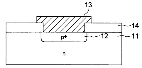
Fig. 1 is a cross-sectional view of a diode which is irradiated by
electrons according to a manufacturing method of the present invention;
Fig. 2 is a graph showing the on-voltage of the diode shown in Fig. 1
when the diode is irradiated by electrons having energy of 270 keV followed by
annealing in a hydrogen atmosphere;
Fig. 3 is a graph showing the measurement results of a current flowing
through the diode shown in Fig. 1 when a voltage applied thereto in the
forward
direction is changed to that in the reverse direction; and
Fig. 4 is a graph showing the integral value of the reverse current with
respect to the change in the forward current when the diode shown in Fig. 1 is
irradiated by electrons having energy of 270 keV followed by annealing in a
hydrogen atmosphere.
If the device is electron-irradiated up to 1 E17/cm2 of dose range or
more, similar results of " electron beam /H+, H2" can be achieved
DESCRIPTION OF THE PREFERRED EMBODIMENTS
In a method for manufacturing a semiconductor device according to the
present invention, a surface of the semiconductor device having a junction
area
formed by doping with a first conductive dopant and a second conductive
dopant is irradiated by particles, such as electrons having energy of 100 to
500
keV or charged particles having energy of several MeV. In addition, the
method described above includes an annealing step that is performed in a
hydrogen atmosphere during or after the irradiation by charged particles. This
annealing step is preferably performed at a temperature of approximately
100°C
to 350°C for 30 to 60 minutes.
CA 02357985 2001-09-28
The method of the present invention decreases electron energy
required for irradiation, stabilizes generated defects by a hydrogen step or
high
dose irradiation, that is, by the annealing step in a hydrogen or hydrogen
plasma atmosphere or by the excessive bombardment of particles, and
effectively decreases the lifetime of minority carriers. The annealing may be
performed by irradiation of the electron beams in the hydrogen atmosphere.
In general, it has been known that electron energy of 500 keV or less is
too low for irradiation by electrons, and that defects formed inside silicon
are
unstable.
In order to solve the problem described above, by performing the
hydrogen step described above, the method of the present invention effectively
decreases the lifetime of minority carriers even by radiating electrons having
energy of approximately 100 to 500 keV.
Silicon atoms are bombarded with electrons and are then knocked out
from the equilibrium positions in the crystal lattice, thereby forming
defects.
Accordingly, a new energy level is generated in the bandgap of the silicon. In
this embodiment, spaces formed by the bombardment of the silicon atoms by
the electrons are called vacancies, and an interstitial atom denotes the atom
existing at a position different from the original position thereof in the
crystal
structure due to the bombardment. Accordingly, when the interstitial atom
recombines with a vacancy, the original state can be recovered.
In the hydrogen step or with high dose irradiation, hydrogen atoms
injected in the silicon interfere with the recombination described above.
Since
electrons having high energy of approximately 2 MeV, which are generally used
for this purpose, can place a silicon atom at a position far away from the
original
position, it is considerably difficult for the silicon atom to return to the
original
position. However, since electrons having energy of 500 keV or less cannot
place a silicon atom at a position relatively far away from the original
position, it
CA 02357985 2001-09-28
6
is relatively easy for the silicon atom to return to the original position,
and hence,
defects already formed are likely to disappear with time or with an increase
in
temperature of the semiconductor device.
The present invention was made in view of the facts described above
and in consideration of the phenomenon described below. That is, defects
formed by electrons having energy of approximately 100 to 500 keV can be
changed into stable defects by a reaction with hydrogen during an annealing
step performed in a hydrogen or a hydrogen plasma atmosphere.
In other words, the manufacturing method of the present invention uses
the phenomenon in that when hydrogen ions are located in the vicinity of the
defects formed by electron beams having low energy, it is difficult for the
interstitial atoms to recombine with vacancies. Accordingly, when the
vacancies are filled with hydrogen atoms, the effect of decreasing the
lifetime by
irradiation by electron beams can be further increased. The same results can
be achieved by high dose irradiation, because excessive bombardment of
particles stabilizes the defects.
As described above, according to the method for manufacturing the
semiconductor device of the present invention, by irradiating the
semiconductor
device with electrons or ionized particles having energy of 100 to 500 keV,
defects can be formed in the semiconductor device, and as a result, an
effective
decrease in lifetime of the minority carriers can be achieved in addition to
the
reduction in facility and production cost.
Referring to Fig. 1, a preferable embodiment of the present invention
will be described in detail. As shown in Fig. 1, an oxide film 14 is formed on
a
surface of an n-type silicon substrate 11. A part of the oxide film 14 thus
formed is removed. A p+ doped region 12 is formed by ion implantation of a p-
type dopant in the n-type silicon substrate 11 at a position corresponding to
that
at which the oxide film 14 was removed. Accordingly, a p+ n-diode is formed.
CA 02357985 2001-09-28
7
A metal electrode 13 is formed on the P+ doped region 12 of the n-type
substrate 11 and on an oxide film 14 in the vicinity of the P+ doped region
12.
Aluminum, molybdenum, gold, silver, or tungsten is used for forming the metal
electrode 13.
According to this embodiment, the p+ n-diode described above is
irradiated by charged particles such as electrons or ionized particles having
low
energy.
Electron beam energy used in this embodiment is approximately 100 to
500 keV. This energy level means that a low-energy electron beam apparatus
which is generally used for irradiating electrons can be used in the present
invention.
When a low-energy electron beam apparatus irradiates silicon lattices
by charged particles, unstable defects are formed in the silicon; however,
according to the data described below, the above-mentioned defects can be
changed into stable defects by a reaction with hydrogen. Hydrogen ions have
significantly high reactivity with the defects described above, and hence,
hydrogen ions can satisfactory combine with the defects which exist at
positions
of a few tens of micrometers from the surface of the semiconductor device.
Accordingly, when hydrogen atoms exist in the vicinity of the defects
(that is, vacancies) formed by low-energy electrons, it is difficult to cause
the
interstitial atoms that were knocked out from their original positions to
return to
the vacancies, and hence, the defects can exist in a stable state.
As described above, since the number of the defects in a stable state is
increased, the lifetime of the minority carriers in the semiconductor device
can
be effectively decreased.
Fig. 2 is a graph showing the on-voltage of the p+ n-diode shown in Fig.
1 when the diode is irradiated by electron beams having low energy followed by
annealing in a hydrogen or a nitrogen atmosphere.
CA 02357985 2001-09-28
8
The on-voltage in the present invention is defined as the forward
voltage drop of a diode when a forward current of 5 mA flows by turning on the
diode.
The diameter of the diode used for the experiment was 100 Vim, and the
resistivity and an annealing temperature were 20 ohm~cm and 300°C,
respectively. The energy of irradiated electrons was 270 keV.
As shown in Fig. 2, the diode annealed in a nitrogen atmosphere has an
on-voltage of 1.41 to 1.47 V in the range of the electron dose shown in Fig.
2.
In the case described above, it is understood that the change in on-voltage
substantially does not occur with an increase in electron dose of this range.
However, when annealing is performed in a hydrogen atmosphere, the
on-voltage is 1.50 to 1.73 V in the same range of electron dose as that in the
nitrogen atmosphere. In the case described above, it is understood that the
on-voltage is significantly increased with an increase in electron dose.
Accordingly, since the forward voltage drop of the diode is increased by
hydrogen, the hydrogen serves to stabilize the defects, and as a result, it
can be
confirmed that the lifetime of the minority carriers is decreased.
Fig. 3 is a graph showing a current flowing through the diode shown in
Fig. 1 when the voltage applied thereto in tt~re forward direction is changed
to
that in the reverse direction in order to verify the turn-off property of the
diode.
In the case described above, the forward current was set to 5 mA.
As can be seen from the graph shown in Fig. 3, it is understood that the
reverse current is increased to approximately 7 mA at a switching time and is
then exponentially decreased.
The reverse current measured at the switching time primarily includes a
current generated by excess minority carriers that are not consumed by
recombination.
CA 02357985 2001-09-28
9
When the total amount of charge of the excess minority carriers, the
amount of charge obtained by integrating the reverse current with time, and
the
amount of charge which is consumed by recombination are represented by Qrr,
Q;, and Qrec, respectively, since Qrr disappears by the counteraction between
the reverse current and the current generated by the recombination, the
equation, Qrr = Qi + Qrec~ holds.
In this equation, Qrr is defined as the integral value of the forward
current in the range of the lifetime of the minority carriers. Accordingly,
when
the forward current is increased, Qrr, Q;, and Qrec described above are
increased in proportion to the increase in forward current.
Fig. 4 is a graph showing the integral value of the reverse current with
respect to the forward current in order to show that the lifetime of the
minority
carriers is decreased when the diode shown in Fig. 1 is irradiated by electron
beams. The diode shown in Fig. 1 has a current property like that shown in
Fig.
3, and the irradiation was performed by electron beams having energy of 270
keV at a dose of 2 x 10¹⁶ electrons/cm2 followed by annealing in a hydrogen
plasma atmosphere. In the case described above, the annealing was
performed at 300°C for 30 minutes.
As can be seen in Fig.4, it is understood that Q;, which is the integral
value of the reverse current of the p+ n-diode with time, is increased with
the
increase in forward current. In the relationship between Q; and the forward
current, the smaller the slope in the graph, the shorter the lifetime. The
reason
for this is that since the total amount of charge of the excess minority
carriers,
i.e, Qrr, is defined as the sum of Q; and the amount of charge that disappears
by
recombination, i.e, Qrec~ and Qrr is proportional to Q;, as shown in Fig. 3,
when
the rate of the increase in Q; with the increase in forward current, that is,
the
slope shown in the figure, is relatively small, it means that the rate of the
increase in Qrr is small.
CA 02357985 2001-09-28
1
Annealing in a nitrogen atmosphere was performed at 300°C for 30
minutes as in the case of that in a hydrogen atmosphere. As can be seen in
Fig. 4, the smallest slope of Q; is obtained by annealing in a hydrogen
atmosphere after the irradiation by electron beams. This result means that the
lifetime of the minority carriers is most decreased by the irradiation with
electron
beams and the annealing in a hydrogen or a hydrogen plasma atmosphere.
When annealing in a nitrogen atmosphere is performed after the irradiation by
electron beams, the slope is approximately equivalent to that obtained when
the
irradiation by electron beams is not performed, and hence, it is understood
that
the decrease in lifetime of the minority carriers is not significant.
Heretofore, the preferable embodiments of the present invention have
been described; however the present invention is not limited thereto. For
example, the present invention may be naturally applied to an n+ n-diode in
addition to a p+ n-diode, and more particularly, may also be applied to all
semiconductor devices having a p-n junction, such as a bipolar transistor
(BIT),
a metal oxide field effect transistor (MOS), an insulated gate bipolar
transistor
(IGBT), and a thyristor.
In addition, the case in which the semiconductor substrate is irradiated
by electrons is described in the preferable embodiments of the present
invention; however, when the substrate is irradiated by charged particles such
as protons (electropositive particle), ionized particles or the like, the same
advantage as that obtained by the irradiation with electrons can be obtained.
According to the present invention, by irradiating a semiconductor
substrate with electrons or charged particles having energy of 100 to 500 keV
and by subsequently performing annealing in a hydrogen or a hydrogen plasma
atmosphere or by high dose irradiation so as to form stable defects in the
semiconductor device, the lifetime of the minority carriers can be effectively
decreased in addition to the reduction in facility and production cost.