Note: Descriptions are shown in the official language in which they were submitted.
CA 02358163 2001-07-04
WO 00/41149 PCT/US00/00355
COIL ARRAY FOR EAS MARKER DEACTIVATION DEVICE
FIELD OF THE INVENTION
This invention relates generally to electronic article surveillance (EAS) and
pertains
more particularly to so-called "deactivators" for rendering EAS markers
inactive.
BACKGROUND OF THE INVENTION
It has been customary in the electronic article surveillance industry to apply
EAS
markers to articles of merchandise. Detection equipment is positioned at store
exits to detect
attempts to remove active markers from the store premises, and to generate an
alarm in such
cases. When a customer presents an article for payment at a checkout counter,
a checkout
clerk either removes the marker from the article, or deactivates the marker by
using a
deactivation device provided to deactivate the marker.
One well known type of marker (disclosed in U.S. Patent No. 4,510,489) is
known as
a "magnetomechanical" marker. Magnetomechanical markers include an active
element and
a bias element. When the bias element is magnetized in a certain manner, the
resulting bias
magnetic field applied to the active element causes the active element to be
mechanically
resonant at a predetermined frequency upon exposure to an interrogation signal
which
alternates at the predetermined frequency. The detection equipment used with
this type of
marker generates the interrogation signal and then detects the resonance of
the marker induced
by the interrogation signal. According to one known technique for deactivating
magnetomechanical markers, the bias element is degaussed by exposing the bias
element to
an alternating magnetic field that has an initial magnitude that is greater
than the coercivity
of the bias element, and then decays to zero. After the bias element is
degaussed, the marker's
resonant frequency is substantially shifted from the predetermined
interrogation signal
frequency, and the marker's response to the interrogation signal is at too low
an amplitude for
detection by the detecting apparatus.
The type of deactivation device which generates the alternating magnetic field
is
referred to as "active", since one or more coils are driven with an a.c.
signal. The coil driving
signal may have either a constant or a declining amplitude. In the former
case, the marker is
swept through the field to provide the requisite decaying waveform as the
marker exits the
field.
1
CA 02358163 2008-02-19
77496-70
There have been proposed a number of coil array
configurations for marker deactivation devices, including a
planar array of rectangular coils (U.S. Patent
No. 5,867,101) or "pancake" coils (U.S. Patent
No. 5,905,435). It has also been proposed to wind the
deactivation coil or coils around a magnetic core (U.S.
Patent No. 6,060,988). These coil arrangements generate a
favorable field distribution, and provide reliable
deactivation of the marker even if it is presented for
deactivation at some distance from the coils. However,
these coil arrangements tend to be somewhat bulky and costly
to produce.
It is known to provide another type of
deactivator, known as "passive", and including an array of
permanent magnets arranged within a housing having a very
low profile. Although these so-called "deactivation pads"
can fit conveniently on a check-out counter, reliable
deactivation requires that the marker be brought very close
to or in contact with the deactivator. This may be
difficult or impossible to accomplish if the marker is
incorporated in the article of merchandise or its packaging,
as is done in the increasingly popular practice known as
"source tagging".
OBJECTS AND SUMMARY OF THE INVENTION
It is an object of the invention to provide a
highly compact device which reliably deactivates
magnetomechanical EAS markers even if the markers are
presented for deactivation at some distance from the device.
It is a further object of the invention to provide
a deactivation device that can be manufactured at low cost.
2
CA 02358163 2008-02-19
77496-70
According to the invention, there is provided an
apparatus for deactivating an EAS marker, including a
plurality of substantially planar substrates in a stacked
arrangement, each of the substrates having formed thereon an
array of spiral coils, the apparatus also including
conductors for interconnecting the arrays of coils, and an
energizing circuit connected to the arrays of coils for
energizing the coils to generate a magnetic field for
deactivating the marker. The array of spiral coils on each
of the substrates may be in the form of a square, six-by-six
array, with each of the coils consisting substantially of
three turns, and the arrays being positioned in registration
with each other in a vertical direction. The number of
substrates may be four, with the arrays of spiral coils on
the substrates being connected to form a six-by-six planar
array of composite coils, and with each composite coil
formed by interconnecting the corresponding spiral coils
from each of the four arrays.
The energizing circuit may be housed separately
from the coils, so that the coil-bearing substrates may be
contained within a housing having a very low profile that
may be conveniently installed on a check-out counter. In
addition, the coil arrays may be produced very economically
by using processes conventionally employed to form
conductive traces on printed circuit boards. Moreover, the
coil array provided in accordance with the invention can be
energized to provide a substantially uniform magnetic field
which extends above the coils at a distance which
facilitates reliable deactivation of markers incorporated in
articles of merchandise.
The foregoing, and other objects, features and
advantages of the invention will be further understood from
3
CA 02358163 2009-05-05
77496-70
the following detailed description of preferred embodiments
and from the drawings, wherein like reference numerals
identify like components and parts throughout.
According to one aspect of the present invention,
there is provided an apparatus for deactivating an
EAS marker, comprising: a substantially planar substrate; an
array of spiral coils formed on said substrate; an
energizing circuit for energizing said coil tracks to
generate a magnetic field for deactivating said marker;
means for connecting said energizing circuit to said coil
tracks; and a housing in which said substrate is contained;
wherein said substrate is one of a stack of a plurality of
substantially planar substrates, each of said substrates
having formed thereon an array of spiral coils; means for
interconnecting said arrays of coils on different substrates
of said stack to form a composite coil.
BRIEF DESCRIPTION OF THE DRAWINGS
Fig. 1 is a schematic vertical sectional view of a
marker deactivation device provided in accordance with the
invention.
Figs. 2A-2D are respective plan views of
deactivation coil arrays included in the deactivation device
of Fig. 1.
Fig. 3 is a schematic diagram of a coil driving
circuit included in the deactivation device of Fig. 1.
Fig. 4 illustrates a current waveform of the
signal applied to the coil arrays by the coil driving
circuit of Fig. 3.
3a
CA 02358163 2009-05-05
77496-70
Fig. 5 is a view similar to Fig. 1 of a marker
deactivation device provided according to an alternative
embodiment of the invention.
DESCRIPTION OF PREFERRED EMBODIMENTS
A preferred embodiment of the invention will now
be described, initially with reference to Fig. 1.
Fig. 1 is a schematic vertical sectional view of a
marker deactivation device 10 provided in accordance with
the invention. The deactivation device 10 includes a
housing 12
3b
CA 02358163 2001-07-04
WO 00/41149 PCTIUSOO/00355
housing 12 includes a substantially flat, planar top surface 14 at or near
which EAS markers
are presented for deactivation. Positioned within the housing 12 just below
the top surface
14 is a vertically stacked arrangement of four substrates 16, 18, 20, 22. As
will be seen, each
of the substrates has formed thereon a coil array. The respective coil arrays
are interconnected
to form a composite coil array which is driven to generate a deactivation
magnetic field at, and
for some distance above, the top surface 14.
Also contained within the housing 12 is a coil driving circuit 24 which is
connected
via cable 26 to the aforementioned composite coil array, (not shown separately
in Fig. 1 from
the substrates 16, 18, 20 and 22).
Another component located within the housing 12 is a detection circuit 28
connected
via a cable 30 to a transceiver coil which is not separately shown in Fig. 1
but will be
discussed below.
It is to be noted that, for ease of illustration, the vertical dimension of
Fig. 1 has been
exaggerated relative to the horizontal dimension. Preferably the housing 12
has a
conventional low profile configuration like known "deactivation pad" devices.
Although coil driving circuit 24 and detection circuit 28 are shown as being
positioned
in the housing 12 below the substrates 16-22, it is contemplated to position
one or both of
these circuits horizontally alongside the substrates and/or in a housing or
housings separate
from the housing 12.
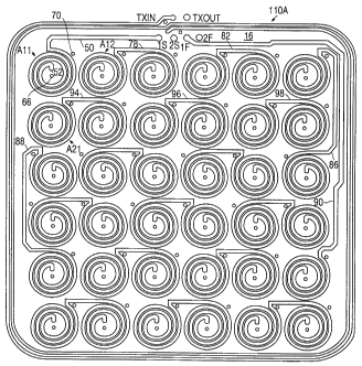
Figs. 2A-2D are, respectively, plan views of the four substrates 16, 18, 20
and 22,
showing conductive traces provided on the substrates to form coil arrays
thereon. Each of the
coil arrays is a square, six-by-six array of spiral coils, each coil
consisting of substantially
three turns. It will be observed that all of the coils are of substantially
the same size and the
center-to-center spacing from one coil to the next (in either the row or
column direction) is
slightly more than the coil diameter. Consequently, the outermost turn of each
coil is almost
tangent to the respective outermost turns of adjacent coils.
The coil arrays respectively provided on each of the four substrates are
positioned
vertically in registration with each other, so that each of the coils on top
substrate 16
(illustrated in Fig. 2A) has a corresponding coil positioned directly below it
on each of the
substrates 18, 20 and 22. As will be seen, vertical connections provided
between the
substrates join each stack of four spiral coils so as to form therefrom a
composite coil. As will
also be seen, the thirty-six resulting composite coils are connected so as to
provide two series
4
CA 02358163 2001-07-04
WO 00/41149 PCTIUSOO/00355
connections of eighteen composite coils each, connected in parallel to the
coil driving circuit
24. -
A first one of the two series coil arrangements is driven via a lead 50 (Fig.
2A) which
is connected to the outermost turn of spiral coil A11, which is the first coil
in the first row on
substrate 16. A central terminal point 52 of coil A11 is conductively
connected through a via
hole (not shown) in substrate 16 to a central terminal point 54 of coil B11
which is the first
coil in the first row on substrate 18 (Fig. 2B). A peripheral terminal point
56 of coil B 11 is
conductively connected through a via hole (not shown) in substrate 18 to
peripheral terminal
point 58 of corresponding coil C 11 on substrate 20 (Fig. 2C). Further, a
central terminal point
60 of coil C l 1 is conductively connected through a via hole (not shown) in
substrate 20 to a
central terminal point of coil DI 1(Fig. 2D). Consequently, the super-posed
coils A11, B11,
C l 1 and D 11 are series-connected to form one of the aforesaid composite
coils.
It will further be noted that the series connection continues via a lead 64
which
connects coil D 11 to a coil D 12 which is the second coil in the first row
and is adjacent to coil
D l 1 on substrate 22. A second composite coil arrangement is formed of super-
posed coils
D12, C12 (Fig. 2C), B12 (Fig. 2B) and A12 (Fig. 2A). In the same manner as
just described,
a series connection is made among these coils A12-D12 from eitlier central or
peripheral
terminal points. Similar vertical-direction connections are provided to form
composite coils
out of the remaining thirty-four stacks of four spiral coils each.
It is also to be noted that dots 66 (Fig. 2A) and 68 (Fig. 2B) correspond to
via holes
provided in registration on all the substrates to accommodate the connection
between terminal
points 60 (Fig. 2C) and 62 (Fig. 2D). Similarly, dots 70 and 72, on Figs. 2A
and 2D,
respectively, correspond to the positions of via holes that allow connection
between terminal
points 56 and 58 on Figs. 2B and 2C, respectively. Likewise, dots 74 and 76,
respectively on
Figs. 2C and 2D, are indicative of the via holes to accommodate the connection
between
points 52 and 54 shown on Figs. 2A and 2B, respectively. The dots appearing in
conjunction
with the other spiral coils are likewise indicative of conductive connections
made in a. vertical
direction among super-posed coils.
The series connection maintained through the composite coils corresponding to
coils
Al 1, etc. and A12, etc. continues via leads 78 (Fig. 2A), 80 (Fig. 2D), 82
(Fig. 2A) and 84
(Fig. 2D), to link together all six of the composite coils corresponding to
the first rows of the
four coil arrays. The series connection is continued to the third rows of the
coil arrays via a
5
CA 02358163 2001-07-04
WO 00/41149 PCT/US00/00355
lead 86 shown on Fig. 2A and then via a lead 88 to the six composite coils
corresponding to
the fifth rows of the coil arrays. The return from the first series
connection, comprising the
eighteen composite coils of the first, third and fifth rows, is provided via a
lead 90. The
connections from coil to coil within each row are also shown but will not be
specifically
discussed.
The initial lead for the second series connection of eighteen composite coils
is
indicated at 92 in Fig. 2D. In like manner to the previously-mentioned rows of
composite
coils, the composite coils of the second rows of the coil arrays are joined by
leads 94, 96, 98
(Fig. 2A) and 100, 102 (Fig. 2D). The series connection continues from the
composite coils
of the second rows to the composite coils of the fourth rows by way of lead
104 shown on Fig.
2D. The series connection continues from the fourth rows to the sixth rows via
lead 106
shown on Fig. 2D. The return path from the second series arrangement
corresponding to the
second, fourth and sixth rows of coils is provided by lead 108.
It will also be recognized from the nature of the connections described above
and the
coil configurations shown in the drawings that all of the individual spiral
coils making up each
composite coil are driven so that current flows in the same direction (i.e.
all clockwise or all
counter-clockwise). Moreover, each composite coil in a row is driven in the
opposite sense
from each adjoining coil or coils in the same row. Also, each coil is driven
in the opposite
sense from the corresponding coil in an adjacent row or rows. Thus, for
example, the
composite coil corresponding to spiral coil A11 in Fig. 2A, is driven in the
opposite sense
relative to the composite coil corresponding to coil A12. Furthermore, the
composite coil
corresponding to spiral coil A11 is driven in the opposite sense relative to
the composite coil
corresponding to spiral coil A2 1, which is the first coil in the second row
of the top coil array.
In a preferred embodiment of the invention, each of the substrates 16, 18, 20
and 22
is formed of a conventional material for printed circuit boards, such as
fiberglass epoxy resin.
All of the traces shown in Figs. 2A-2D are preferably four-ounce copper,
formed by
deposition on the respective substrate and then etching away to provide the
indicated pattern.
For the spiral coils and leads referred to above, the track width is
preferably 65 mils. The
diameter of each of the spiral coils is, in a preferred embodiment, about 0.75
inch,
corresponding to about one-half the length of the type of magnetomechanical
EAS inarker
which the apparatus is designed to deactivate.
6
CA 02358163 2001-07-04
WO 00/41149 PCT/US00/00355
It should be understood that each of these parameters is subject to variation.
Thus, the
width and/or thickness of the copper traces may be changed, and the diameter
of the spiral
coils may be increased or decreased (although it is believed that a diameter
of substantially
one-half the length of the magnetomechanical marker to be deactivated is
optimal). It is also
contemplated to provide more or fewer than the four layers of spiral coil
arrays shown herein.
For example, only one layer (i.e. only one substrate) may be provided, with
suitable
connective traces being provided on the underside of the substrate. Conductive
materials
other than copper may be employed, and other types of substrate materials
besides fiberglass
epoxy resin may be used. The number of composite coils may be less than or
greater than the
thirty-six shown, and the coil arrays need not be square. For example, non-
square rectangular
arrays are contemplated, as are triangular arrays and other shapes. Moreover,
the number of
turns in each spiral coil may be greater than or less than the three turns
shown.
Another notable feature of the trace patterns shown in Figs. 2A-2D is that
each of the
four square arrays of spiral coils is circumscribed by a two-turn coil,
indicated, respectively,
at 110A, 11 OB, 110C and 110D, in Figs. 2A-2D. The coils 110A-110D are
connected in
series by means of via holes (not shown) in substrates 16, 18, 20 so that the
four
circumscribing coils together are connected to form a single, composite
transceiver coil. The
transceiver coil is connected by the above-referenced cable 30 (Fig. 1) to the
detection circuit
28. The detection circuit 28 functions, in accordance with conventional
practice, as a
"doublecheck" circuit to determine whether markers presented for deactivation
have in fact
been deactivated. As is well-known to those who are skilled in the art, the
"doublecheck"
function consists of interrogating the markers by means of an energizing
signal, and then
detecting a ring-down signal generated by the marker in the case that the
marker has not been
properly deactivated. The transceiver coil is used to transmit the marker-
energizing signal,
and to pick up any resulting signal generated by the marker. If a still-active
marker is
detected, an audible and/or visible warning is given. The functioning and
arrangement of the
detection circuit 28 are conventional, and therefore will not be described
further. It is
contemplated to omit from the deactivation device 10 either or both of the
detection circuit
28 and the composite transceiver coil formed of the coil traces 110A-110D.
Details of the coil driving circuit 24 will now be described with reference to
Fig. 3,
which is a schematic diagram of the circuit.
7
CA 02358163 2001-07-04
WO 00/41149 PCTIUSOO/00355
As seen from Fig. 3, a conventional AC power line signal provided at a
terminal 200
is connected to primary windings 202, 204 of a transformer 206 by way of an on-
off switc-h
208, conventional protective circuitry 210 and a switching arrangement 212.
The switching
arrangement 212 allows the coil driving circuit 24 to function either with 110
volt or 220 volt
input power. A secondary winding 214 of the transformer 206 supplies the power
signal after
it has been stepped up or down, as the case may be, to a nominal level of 140
volts AC. This
signal is rectified at diode bridge 218 and then applied, through appropriate
connecting circuit
elements, to charge storage capacitors 220, 222, which are connected in
parallel to diode
bridge 218 and in a manner to charge the capacitors to opposite polarities.
The other secondary winding 216 of the transformer 206 is connected, via a
diode
bridge 224, to logic power supply 226.
Storage capacitor 220 is connected to one of the two series arrangements of
eighteen
composite deactivation coils by one pole of terminal set 228. The other pole
of the terminal
set 228 connects that composite coil series arrangement to ground via triac
230. The other
series arrangement of eighteen composite coils is connected to the other
storage capacitor 222
by way of one pole of terminal set 232. The other pole of the terminal set 232
connects the
second series a.iTangement of composite coils to ground via triac 234.
The coil driving circuit 24 is completed by timing circuitry 236 which
controls the on
and off states of the triacs 230 and 234 by means of triac drivers 238, 240,
respectively.
It will be understood from Fig. 3 that when the triacs 230, 234 are in an open
condition, the deactivation coil arrangements are essentially out of the
circuit, and when the
triacs are in a closed condition, each of the parallel deactivation coil
arrangements forms a
respective resonant circuit with its corresponding storage capacitor 220 or
222, to permit the
charge on the storage capacitor to dissipate as a ring-down signal which
energizes the
respective deactivation coil arrangement. The energized deactivation coils
generate a
declining-amplitude alternating magnetic field at and above the top surface of
the deactivation
device 10.
In operation, the timing circuit 236 and drivers 238, 240 cause both triacs
230, 234 to
be closed simultaneously and then opened simultaneously at a predetermined
timing. The
resulting current waveform induced in both of the deactivation coil
arrangements is shown in
Fig. 4. It will be noted that the waveform is a sequence of isolated ring-down
pulses,
separated by intervals during which the triacs are in an open state and the
deactivation coils
8
CA 02358163 2001-07-04
WO 00/41149 PCT/US00/00355
are not driven. (For purposes of illustration, the time scale of the ring-down
signal pulses is
exaggerated relative to the intervening periods when no drive signal is
applied, and the
number of cycles within each pulse is also exaggerated.) According to a
preferred
embodiment of the invention, the repetition rate of the ring-down signal
pulses is substantially
10 Hz, the ringing frequency is about 12 KHz, and the duration of each pulse
(time to decay
to substantially zero amplitude) is about 300 microseconds. Given the
repetition rate of 10
Hz, it will be understood that the ring-down signal pulses are commenced at
regular intervals
of one-tenth second.
It will be noted from Fig. 3 that the capacitors 220, 222 are constantly being
charged.
The repetition rate of the coil driving signal, the voltage provided by the
secondary winding
214, and the component values are selected so that, at the time each driving
signal pulse
begins, the capacitor is charged at least to an adequate level to provide a
deactivation field of
sufficient amplitude to deactivate markers presented within a predetermined
distance of the
top of the deactivation device. The maximum charge applied to the capacitors
220, 222 is
limited by the peak voltage supplied through secondary winding 214. Because
the minimum
charge to the capacitor is determined by the timing at which the triacs are
closed, and the
maximum is limited by the charging signal level, no voltage regulator is
required.
It has been noted above that the nominal output of the secondary winding 214
is 140V
AC. Because the actual input AC power may vary from the nominal 11 OV or 220V,
the actual
signal level applied to diode bridge 218 may be in the range 120 to 160V
(RMS), and the
maximum DC level applied to the capacitors 220, 222, and hence the maximum
charge level
of the capacitors, may be about 180 to 230 V.
Because of the relatively rapid repetition rate of the deactivation signal
pulses, a
magnetomechanical EAS marker presented at the top surface of the deactivation
device is
likely to be subjected to at least several ring-down signal pulses, thereby
providing highly
reliable operation.
The coil driving circuit disclosed herein may be modified in numerous
respects, or
may be replaced with a circuit which drives the coil array with a fixed-
amplitude alternating
signal. For example, the coil array may be driven from the input power line
via an isolation
transformer arranged to step the input power up or down to a desired level. If
a fixed-
amplitude driving signal is employed, then markers presented for deactivation
are to be swept
past the deactivation device.
9
CA 02358163 2001-07-04
WO 00/41149 PCTIUSOO/00355
A marker deactivation device provided according to an alternative preferred
embodiment of the invention is generally indicated by reference numeral 10' in
Fig. 5. The
stacked substrates 16, 18, 20, and 22 are the same as in the embodiment of
Fig. 1, including
the coil arrays which have previously been described. The detection and coil
driving circuitry
is not shown in Fig. 5, and may be provided in a separate housing which is
also not shown.
The embodiment of Fig. 5 features a magnetic shield member 40 positioned below
the
stackcd substrates in the housing 12' of the deactivation device 10'. The
shield member 40
is preferably thin, planar, and horizontally oriented, and may be made of a
suitable material
such as 430 stainless steel or pressed powdered iron. If made of stainless
steel the shield
member 40 may be about 1 mm thick; if made of pressed powdered iron it may be
2 mm
thick.
As will be understood by those who are skilled in the art, the purpose of the
shield
member 40 is to change the shape of the magnetic field generated by the coil
array so that the
magnetic field is enhanced at positions above the top surface 14 of the
housing 12'.
If the frequency of the coil driving signal is relatively low, say 2 kHz or
less, then
stainless steel is the preferred material for the shield 40. If the driving
signal frequency is
relatively high, i.e. in the kilohertz range up to 250 kH--,, then pressed
powdered iron is
preferred.
Various other changes in the foregoing apparatus may be introduced without
departing
from the invention. The particularly preferred embodiments of the invention
are thus intended
in an illustrative and not limiting sense. The true spirit and scope of the
invention are set forth
in the following claims.