Note: Descriptions are shown in the official language in which they were submitted.
10/01/01 17:48 FAX 804 881 4081 ~ op398169"2'001-io-0111 f~004
METHOD AND APPARATUS FOR ILLUMINATING
A SPATIAL LIGHT MODULATOR
FIELD OF THE INVENTION
The invention disclosed herein relates generally to the field of semiconduc
:or
laser diodes and more particularly to semiconductor laser diodes which have
lint. r
arrays of emitters. The invention relates particularly to methods and
apparatus it which
laser radiation output of two or more such diodes is combined to illuminate a
spay ial
liglxt modulator.
BACKGROUND OF THE INVENTION
Semiconductor laser diodes axe used in many applications where compact ~,ize
and/or high efficiency is important. Semiconductor laser diodes offer
relatively l.~w
cost, high reliability and simplicity of usc.
Single emitter mufti-mode laser diodes are commonly available in various
wavelengths with radiation power output up to 2 Watts or more. These lasers
ryl~ically
z o hare a rectangular ox stripe emitter azou~7d I pm high and in the region
of 20 ~.m ~ 50 0
~cm long. Fundamental problems of heat removal and optical emitter facet dama~
a place
an upper limit on the power per unit length of etr~ittex that can be extracted
witho rt
significantly reducing the operating lifetime of such laser diodes.
To use diode lasers in applications that need more than a few Watts of rat
iation
power it is common to use an array of single emitter diodes. It is possible to
form such
an array using single emitter diodes mounted in a mechanical support but it is
me re
common to fabricate the array of emitters on $ monolithic substrate. These
devic ss,
10/01/01 MON 19:49 [TX/RX NO 7455] 1~J004
10/01/01 17:49 FAg 804 881 4081 ~ pp358169~~2ooi-lo-o111. ~ 005
a
s known as laser diode bars, are available in many configurations with
radiation po wet of
up to 50 Watts. Laser diode bars have found application in machining, welding
~~:
soldering, medical, imaging, pumping for solid-state lasers and many other
applic ations
that require low cost, reliable, compact radiation sources.
A monolithic laser diode array 1 is shown in FAG. 1. It consists of a
1 o semiconductor substrate 2 upon which is formed an array of emitters 3 _
Adjacen
emitters have a dead space between them that does not emit light. Due to
emitter
geometry, the radiation beam 4 is substantially asymmetrical while also having
di I feting
divergence rates in the x-axis and y-axis directions. The full width
divergence in the y-
axis is typically in the range of 40° to 100° and in the x-axis,
8° to 20°. because c ~ f the
is high divergence, the y-axis is often referred to as the "fast" axis while
correspond Lingly
the x-axis is referred to as the "slow" axis. The high beam divergence of
semiconductor diode lasers makes it necessary to collimate or focus the beams
en ~ fitted
by such lasers for most applications.
The beam quality in the y-axis can be very good, with an MZ value of clos ~~
to
2 0 1Ø lv,(i is a dimensionless pararxxeter that characterises the degree of
imperfectio a of a
laser beam. An ideal, diffraction-limited, Gaussian profile beam would have an
] ~~~z of
1_0_ Any departure from the ideal results in an Mz value of greater than 1Ø
Th;~ Mz
of the beam from a laser diode in the x-axis is very poor, signifying a
substantial
deviation from a perfect beam. This difference in the beam quality, along with
d a
25 differing divergence rates for the x and y axes, make it necessary to treat
the axe;.
separately when designing a collimation scberne.
10/01/01 MON 19:49 [TX/RX NO 7455] I~J005
10/01/01_ 17:49 FAX 804 8_81 4081 ~ pp358169'~2ooi-lo-ollL ~J008
3
Spatial light modulators offer an advantage in imaging in that they can be
fabricated as raulti-channel devices, thus reducing system complexity v~rhile
i~ncref ping
imaging speed. Spatial light modulators arc optical modulators constructed to
spa .ially
modulate, according to prescribed input, a readout apticai beam. Spatial light
modulators having a single line of modulating elements or areas are of
particular ~ use in
1 o imaging tasks although in some applications multi-line devices can also be
advantageous. Exa~aaples of spatial light modulators include a Wide rair~ge of
electro-
optical, acousto-optical, and ele~txomechanical devices.
''bile laser diode bars have several advantages for illuminating a spatial
li,~ht
modulator one must first overcome the challenges set the by fox'~nat of the
laser d ode
1 s beam. For optimal illumination of a line spatial light modulator, the
laser bar rac iation
must be precisely transformed into a line of uniform illumination in a manner
Thai
maximizes brightness. Brightness is defined as the luminous flux emitted from
a
surface pex unit solid angle per unit of area_
Commonly assigned patent US 5,51.7,359, to Gelbart discloses a method c~f
z o formatting the output from a ]user diode to form a line source
particularly useful 'or
illuminating a spatial light modulator. Radiation fzom each emitter is fully
overly Aped
at the modulator in both the x and y axes_ A cylindrical microlens collimates
the
radiation in the y-axis. In the x-axis an array of cylindrical microlens
elements
collimate and steer the radiatiozt towards a common target point, some
distance fi om the
25 laser, overlapping the radiation profiles.
10/01/01 MON 19:49 [TX/RX NO 7455] f~J006
10/01/01 17:50 FA$ g04 B81 4081 ~~'°"' ° 1007
CA 02358169 200110-O1 ~L
4
The overlapping of emitter radiation profiles is advantageous should one o '
more
emitters fail_ Since the overall profile is the sum of a plurality of
emitters, an em tter
failure only reduces po~xrer and does not substantially change the profile_ In
contt.~st, if
only the fast axis is collimated and the slow axis is allowed to diverge up to
a pov i t
where the beams overlap only partially, an emitter failure will severely
compromi;~e the
1 o profile. Another advantage of overlapping is that dead space between
emitters is
effectively removed, creating a high brightness illumination line.
A problem that occurs in using many laser diodes bars is that, as a result c F
stress-induced bending of the device wafer, the emitters are not in a
perfectly stra i ght
line; a characteristic known as "smile" _ While bars have been manufactured
witl sub-
miCrOn Smlle, it is more common to have to deal with around 5 - 1 0 m of
smile. A
non-negligible smile prevents precisely aligning the beams in the y-axis and
thus
degrades line quality. In commonly assigned US patent No. 5,861,992 to Gelbar
an
individual rnuc~colens is mounted in front of each emitter. The mierolens is
adjust 'd in
tb.e y-axis direction to line up all emitter radiation profiles at a target
plane_ In tb~s case
2 o the microlenses also perfoxxn collimation of the emitters in both axes and
addition ally
can be used to steer the emitter profiles to overlap in, the x-axis direction_
The
microlenses are individually sliced from the centre of a moulded asphexic
lens, su ~"b, that
each slice is substantially the same as the diode array pitch.
Advances in semiconductor materials have lead to the available power from
laser
2s diodes bars more than doubling over the past few years. However, despite
these
advances, it is unlikely that there will be a further doubling of power levels
in the near
10/01/01 MON 19:49 1TX/RX NO 7455] I~]007
10/01/01 17: 50 FAg 604 681 4081 <'~" ' f~ 008
CA 02358169 2001-10-O1 ~L
5 future unless there is a significant breakthrough in the art. On the other
hand,
applications continue to demand higher overall laser powers.
US patent No. 4,71,(,568 discloses a plurality of linear diode laser array
subassemblies stacked one above the other and simultaneously powered frorza a
single
source. In this configuration, power can easily be scaled by simply adding
more laser
1 o diode arrays. The downside is that it is very difficult to design
combination syste ms
that deal witb~ the radiation asymmetry while simultaneously preserving
brightness ~ for a
vertical stack. While this combination sclaezne is effective at increasing the
powe
available, the loss of brightness counters much of the gain, particularly for
demai ding
innaging applications.
US patent No. 6,240,116 discloses a stepped reflector that can be used to
combine beams from multiple laser diodes, simultaneously correcting some of
the
asymmetry while conserving brightness _ However the stepped reflector is a
comb ~~lex
component to manufacture and will have a significant impact on system cost and
complexity. ,Additionally it is still necessary to individually microlens each
emitt er to
zo achieve a good profile.
Accordingly, there is a need for apparatus and methods for combining the beams
from two or more laser diode arrays to achieve higher power than is available
frc m a
single bar diode_ There is a parricular need for such irinethods and apparatus
whit h:
~ combine the radiation in such a way that bzightness is maximized;
10/01/01 MON 19:49 (TX/RX NO 7455] f~J008
10/01/01 17:50 FAX 804 881 4081 ~ op358169~2'001-io-oi,L f~009
6
~ minimise the additional cost and complexity involved in producing a
combined laser array source;
~ preserve the beam quality in the y-axis so that a substantially Gaussian
profile is maintained; and,
~ combine the beams in such a manner that the far field pzofiles are
to substantially uniform in the x-axis.
~Y OF THE INVENTION'
This invention provides methods for constructing high power, high quality ,
and
high brightness illumination souzces for spatial light modulators from two or
more
multiple emitter laser diode arrays. The invention also provides appazatus for
z 5 illuminating spatial light modulators and systems which incorporate such
apparatt s. By
mounting two laser diode arrays adjacent to each other and providing optics
oper:~tive to
collect and steer the radaataon towards a target plane the radiation of two or
more Caser
diodes can be combined while maintaining beam quality and brightness.
BRIEF DESCRIPTION OF THE DRAWINGS
a o In draw~gs vyhich illustrate non-limiting embodiments of the invention:
FfG~ 1 depicts a generic prior art laser diode array;
FIG. 2 is a graphical depiction of the far field profile of an idealized line
;:flurce;
FIG. 3 depicts a particular embodiment that combines the radiation from t ~wo
iuadividual lasez diode bars to form a single high power line source;
10/01/01 MON 19:49 [TX/RX NO 7455] 1~J009
10/01/01 17: 51 FAX 6o4 681 4081 ~«°w, ~. f~ 010
CA 02358169 2001-10-O1 ~L
7
FIG_ 4 depicts an embodiment of the invention that combiuoves the radiation
from
two laser diode bars using microlenses associated with each emitter;
FIG. 5 depicts an alternative embodiment of the invention advantageous in
reducing off-axis aberration from the microlenses; and,
FIG. 6 depicts an embodiment of the invention that combines two laser diode
1 o arrays on a common base_
DESCRIPTION OF 1'DE PREFERRED EMBODIMENT
This invention involves connbining the radiation of two or more laser diod :
bars,
More specifically the invention relates to Combining the radiation of two or
more diode
bars where the bars are mounted side by side. Collecting optics are placed in
fro it of
1 s the bars to format and direct the radiation to foz-m a radiation profile.
In this disclosure tlxe texxn "laser diode array" or "array" refers to an arts
~r of
emitters on a monolithic semiconductor substrate. The term "laser diode bar"
or 'bar"
refers to a "laser diode array" , permanently mounted on a base. The base
provid ~~s for
mounting electrical connections and/or heat removal. The product sold by most
1 user
2 o diode vendors is a "laser diode bar" as described above. Where the
distinction is
immaterial, the device will simply be referred to as a "laser diode" or just
"laser" _
Furthermore, the term "optical element" refers to any element operati~'e t. ~
change the properties of a beams of light. A lens is an example of an optical
elem ~~nt. A
mirror is another example of an optical element. The term "microlens" is used
t' ~~ refer
25 to an optical lens element of small size.
10/01/01 MON 19:49 [TX/RX NO 7455] [~JO10
ioioi/oi 17: 51 FAX 804 881 4081 ~«~~T ~~ f~ 011
CA 02358169 2001-10-O1 ~L
8
Furthermore, the terms "cohecting optics" or "collecting" aze used to denote
the optics or the process of gathering diverging light from a source, such as
a set rf
laser diode emitters and fozzning a collimated or converging beam o~F light
along a
unidirectional path towards a target plane. Although the light may be focussed
at the
target plane, this is not necessarily required in the aforegoiz~g definition.
i o FIG. 3 shows a pair of laser diode bars 15 each cozaaprising a laser diode
f tray 2
mounted on a base 20. A cozamo~a zoicrolens 21 collects the y-axis radiation
for 1 4th
lasers. Miczolens array 22, comprising microlenses 23, collects the x-axis
radiati;~n
from each emitter. Microlenses 23 are also opezative to steer beams 24 from
cad
emitter in the x-z plane, forming an overlapped line profile 25 at a point
some dis i ance
away from diode bats 15. Laser diode bars 15 and optical elements are mounted
c.a a
rigid support base (not shown).
FIG. 2 shows an idealized profile of an illumination line suitable for
illuminating a spatial light xzaodulator_ )fzt the y-axis direction, the beam
is formed into
to a narrow substantially Gaussian profile 10_ In the x-axis, all ernittezs
have bee i
zo ovezlapped to form a line with the characteristic top-hat shape 11. The
overlappe,l
profile will typically hare less va~~on than individual emitter profiles and
is thu ~~
effective in smoothing out random variations in emitter profiles.
The bars 15 shown in FIG. 3 are an example of a narrow package bar, which is
not much wider in the x-axis than the diode array chip, facilitating close
side-by-~ ide
z5 mounting. An example of such a bar is supplied by Coherent Inc of Santa
Clara,
California under part number B1-83-SOC-19-30-B. This laser diode hat is a
fluid
10/01/01 MON 19:49 [TX/RX NO 7455] I~ 011
ioioi(oi 17:51 FAX 804 881 4081 ~ 02358169"2001=l0-0lll. ~ 012
9
cooled SOW bar comprising 19 emitters with a 30% fill factor. Fill factor is
defin ~ as
the percentage of the x-axis array dimension filled by radiation emitting
emitters. The
method of cooling of the diode bar could be convective, conductive or fluid
based and is
not directly material to the present invention.
The microlens element 21 is an optical element suitable for collimating the
fast
1 o axis of a laser diode bar. It must be able to collect the high numerical
aperture be ~tzus
from the laser emitters in tlxe y-axis without significant degradation in the
beam quality.
A specially designed spherical, aspherical or a graded index element may be
need 'd for
a specific set of design considerations. Microlenses for fast axis collimation
are
available from Blue Sky Research (Milpitas, CA), LIMO - T~issotschenko Mikroo
~tik
Gmb~ (Dortmund, Germany) and NSG America, lnc (Somerset, NJ).
The microlens array 2Z is azt array of microlenses at a fixed pitch determi~
red by
the emitter geometry_ The degree of overlap between the emitter radiation
profilf s is
selected by choosx~ug the pitch of the microlens array to be less than the
pitch of ti ~ a
emitters on the laser diode array. A microlens pitch slightly less than, the
emitter pitch
z o will steer the radiation firoxn outer emitters towards a central target
point causing i he
orrerlap_
Regardless of how close together bar packages 1.5 are mounted, these will be
some dead space between them that must be taken into account. It is possible
to ~ i se
two individual microleas arrays but it is cheaper and siyonpier to use a
single array
25 element where a few microlenses in the centre are not used. for example, a
1 cni laser
diode array r~ritl~ 19 emitters spaced 500 m apart the spacing between
adjacent
10/01/01 MON 19:49 [TX/RX NO 7455] ~ 012
_ _ ._ 10/01/01 1_7; 52 FAX 804 881 4081 ~ Op358169~~2001-10-O1 1L C~] 013
5 microlenses will be slightly less than 500 tr~_ A 2 mm dead space between
bars a ould
result in not using four of the microlenses.
There are several options for aligning the bars and collimation optics. One
possibility is to fix the t"xrst bar and align the collimation optics to this
bar to achie ve the
desired Iine profile 25 at a target plane_ Once aligned, the collimation
optics are i xed
to in place, and the second bar aligned to produce substantially the same line
profile ;vt the
target plane. ,Another possibility is to fix the position of the collimation
optics arc I then
align both bars to the optics. Regardless of the method chosen there may be
the n;~ed
for iterative alignment where it is necessary to coarse align each element and
then more
finely align the elements in a second or even third pass.
An advantage of the present embodiment is that the laser diode bars are iv
ulable
as standard items. Anotler advantage of this embodiment is that the beam
quality is
maintained izt the fast axis, while doubling the ava~able power and maxim
brightness_
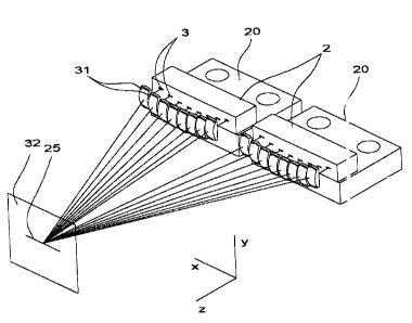
Another embodiment of the present invention shown in FIG. 4 is particularly
z o advantageous in correcting misalignment between the bar diodes in the x-y
plane . ~ s well
as correcting deviations from straightness of the laser emitters. In FIG. 4,
Iaser c iode
arrays 2 are each mounted on a base 20. Individual xnicrolenscs 31 are placed
in liont
of each emitter of laser diode arrays 2. The microlenses are aligned in the y-
axis
direction to direct all emitter images towards line 25 on a target plane so
tl~tat tb,ey
averlap in the y-axis direction. At the same time the lines are overlapped in
the x axis
10/01/01 MON 19:49 [TX/RX NO 7455] 0 013
10/01/01 17:52 FAg B04 B81 4081 ~ op358169~2001-io-oi,L f~ol4
ii
s dizection at the target plane, either partially or completely, by aligning
each micro ens
- 31 in the x-axis .
An advantage of this embodiment is that the radiation from each emitter is
individually aligned allowing very precise overlapping at a target plane. With
earn, an
extremely tight overlap can be achieved maximizing brightness.
1 o Yet another embodiment shown in FIG. 5 is advantageous for a configurat on
where the distance between the target plane 32 and micralenses 31 is reduced
thus
increasing the steering angle for outer emitter microlenses. These microlenses
ha~~e to
provide much more steering towards the target than central microlenses. This
me; i us
that these outer microlenses end up aligned well off their optical axis
resulting in c ~ff
15 axis optical aberrations. The aberrations can degrade the uniformity of the
line pr Mile,
which will likewise degrade the combined profile of all emitters.
In FIG. 5 an optical element 40 is introduced in front of the microlens arrf y
that
has the effect of steering the radiation towards the centre of target plane 32
for our ~r
emitters while having lesser effect on inner emitters. In this embodiment the
micr dens
z o elements 31 are not required to steer the radiation in the x-z plane since
this steeri tg is
now mostly provided by optical element 40. Microlens elements 31 can still
prow: ~,Ie
minor corrections to steering but off axis aberrations are reduced by the
inclusion of
optical element 40.
The optical element 40, as described, can also be added to the embodiment
25 depicted in FIG. 3 or any of the other embodiments detailed in this
disclpsure. );x~ each
10/01/01 MON 19:49 [TX/RX NO 7455] X014
10/01/01 17:5a FAg 804 881 4081 ~ Op358169~~2001-10-O1,L ~ olg
12
s case, the addition of element 40 reduces the ~ steering requirement on the
microlens
elements, thus reducing off axis aberrations from outer emitter/microlens
combinations.
Yet another embodiment is depicted in FIG . 6, which has the advantage of
combining two laser diode arrays in a snn~gle package_ This embodiment is
useful n
situations where space limitations are severe or where long-term stability of
the dig .de
io bar position is a critical issue. The dead space between adjacent bars can
also be
fuxtber reduced since the array positioning is now only dependent on array
placem,:nt
tolerances and not additional mechanical mounting tolerances. The common base
tlso
provides improved long-term stability of the relative bar positions since, in
genera ,
array bonding processes will result in lower long term drift than
mechanuically ~nnoi nting
is two separate packages. The term "bonding" is used to indicate a process
whereby the
laser diode array is permanently fixed to a base_ Improved stability is
important vi
cases where the collimating optics are very sensitive to misalignment or when
the
absolutely highest line quality is sought.
In FIG 6 two laser diode arrays 2 are permanently bonded to a common ba ~e
zo 50_ The collimating elements are shown split into two pieces 21 and 21', 22
and ;;t'.
The need to split the optical elements for collimating each laser diode array
depend Is on
the optical sensitivity of the collimating elements and the mounting accuracy
of the'
arrays_ It is unlikely that laser diode array mounting tolerazzces can be
controlled o a
degree v~ihere a single element can be used as was shown in the previous
embodim;:nt of
2s FIG. 3. Because the arrays are in fixed orientation after bonding any
alignment a ror
10/01/01 MON 19:49 [TX/RX NO 7455] 1~J015
-__ lo/ol/ol 17: 5a FAg 604 881 4081 ~ 02858169--2001-10-O1 iL ~ olg
13
between the trxro bars could not be eliminated if a one-piece collimation
element w~ ~ rc
used_
The collimating schemes of the embodiments shown in FIG. 4 and FIG. 5 ~~an
also be applied to the embodiment shown in FIG. 6. In this case individual
micro: eases
are simply aligned to collect and direct the radiation from each emitter to a
target.
to It should be understood that the above descriptions of the preferred embodi
rents
are intended for illustrative purposes only, and are not intended to limit the
scope . ~f the
present invention in any way. Those skilled in the art will appreciate that
various
modifications ca.a be made to the embodiments discussed above without
departing ;rom
the spirit of the present invention_
10/01/01 MON 19:49 1TX/RX NO 7455) ~JO16