Note: Descriptions are shown in the official language in which they were submitted.
CA 02358332 2001-10-05
502P40CA-1
SIMPLE METHOD OF ALLOWING RANDOM ACCESS TO RAMBUS DIRECT
DRAM FOR SHORT BURSTS OF DATA
Field of Invention:
The present invention relates to computer
memories and, more specifically to methods and devices for
adapting computer memories to computer network
applications.
Background to the Invention
Computer memories have been used in computers
since computers were first invented. The advent. of
networks of computers has provided another field in which
1o computer memories can be used. The increasing rates of
data influx in networks has underlined the difference
between how computers and networks use computer memories.
Previously, high speed yet costly SRAM (Static Random
Access Memories) were used in buffers in computer network
elements to help the networks cope with fast input and
throughput of data in networks. In recent years cheap yet
faster and faster DRAMS (dynamic random access memory)
have taken some of the duties of the SRAM. Because of its
cost, this DRAM type of computer memory is, currently the
2o most widely used type of computer memory in regular
computers. However, as noted above, computers and network
devices use computer memory in different ways.
While regular computers and network devices try
to take advantage of the large storage capacities and fast
access times offered by DRAMS, the patterns of use of
computer memories is different. For computing
applications, long, variable bursts of data are not
uncommon. Furthermore, the amount of data accessed in
2
CA 02358332 2001-10-05
read/write memory access operations and the ratio between
read memory access operations and write memory access
operations is dependent on the actual computer
application. Also, computer applications may require that
computer memories be able to transfer large amounts of
data in a short amount of time even though normal computer
applications generally only use moderate amounts of data
flow. And lastly, data delay, or the delay between bursts
of data, is not a high priority for computer applications.
to In contrast to the above, networking
applications, as implemented in network devices, have very
different requirements. Networking applications generally
require short, fixed length blocks of data from the
computer memories. The amount of data per unit time that
computer memories have to deliver is dictated by datapath
speeds and there are usually equal numbers of read and
write memory access operations. Furthermore, networking
applications require that a guaranteed amount of data be
delivered in a given time to maintain datapaths. In terms
of data delays, delays must be predictable and minimizing
such delays is highly desirable.
One major development in the field of DRAMS is
the emergence of the RDRAM (RambusTM Direct Dynamic Random
Access Memory) device. While the RDRAM does have some
characteristics which would be highly desirable for
networking applications, SllCh as high storage density,
high data transfer capabilities and low amounts of delay
on transitions between read operations and write
operations, the RDRAM is generally considered as being
optimized for computer applications. Like most DRAMS, the
RDRAM is generally most efficient when dealing with long
bursts of data from consecutive memory locations. To this
end, sense amplifiers, used to transfer data to and from
3
CA 02358332 2001-10-05
data banks in a RDRAM, are shared between memory banks.
This design choice allows large chunks of data to be read
out but also prevents an accessed bank, and any banks
adjacent to the accessed bank, from being accessed for a
given amount of time. Thus, if Bank A is accessed, that
bank and any banks adjacent to it cannot be accessed for a
time period that may be as long as the time it takes for
three memory access operations.
This drawback of RDRAMs needs to be overcome so
1o that the benefits of RDRAM can be harnessed for networking
applications.
Summary of the Invention
The present invention seeks to meet the above
need by providing methods and devices for arranging memory
access operations to minimize memory bank conflicts
between such operations. A fixed pattern of memory access
operations is implemented to minimize the effects of a
transition between a read memory access operation and a
write memory access operation. A write-read-gay (WRG) set
2o pattern of a write memory access operation followed by a
read memory access operation and then followed ~y a set
gap when no memory access operation may be undertaken,
meets the particular requirements of RDRAM. Within the
WRG pattern, read addresses and write addresses are
selected to minimize memory bank access conflicts. Such
selections are assisted in increasing the efficiency of
the memory access operations by defining a set frame size
of a specific number of repetitions of the WRG pattern.
All memory access operations are then rearrange~~ to
3o conform to the WRG pattern and, the repetitions of the WRG
pattern are divided into frames having a size equal to
that of the defined frame size. Within each frame, the
read addresses to be accessed by read memory operations
4
CA 02358332 2001-10-05
can be rearranged to minimize memory bank access conflicts
with either write addresses to be accessed by wz-ite memory
operations or other read addresses.
In a first aspect, the present invention seeks
to provide a method of increasing the efficiency of memory
access operations to a memory subsystem having multiple
memory banks, the method comprising arranging memory
access operations to the memory banks such that the memory
access operations follow a predetermined repeating
1o pattern, the repeating pattern comprising a write memory
access operation followed by read memory access operation,
each repetition of the repeating pattern being followed by
a set time gap of during which no memory access operation
may be undertaken, the set time gap being a fixed,
predetermined amount of time.
In a second aspect the present invention
provides a method of selecting a write address for a write
memory access operation to avoid possible memory bank
contention between successive memory access operation the
2o method comprising selecting a write address based on the
following criteria:
a> if a proximate read memory access operation
is executed within a predetermined number of memory access
operations from the write memory access operation, the
write memory access operation accesses a group of memory
banks different from a group of memory banks accessed by
the proximate read memory access operation;
b) the write address accesses a memory bank
chosen from a pool of memory banks, the pool excluding any
of the following:
bl) memory banks accessed by an immediately
preceding read memory access operation;
5
CA 02358332 2001-10-05
b2) memory banks to be accessed by an
immediately succeeding read memory access
operation;
b3) memory banks accessed by an immediately
preceding write memory access operation;
and
b4) memory banks immediately adjacent
memory banks referred to in bl), b2) and
b3 ) ;
1o c) the write memory access operation accesses a
memory bank that is a least full memory bank in the pool
of memory banks.
In a second aspect the present invention
provides a method of increasing an efficiency of read
memory access operations by avoiding possible memory bank
contention between read memory access operations, the
method comprising:
a) arranging memory access operations to the
memory banks such that the memory access operation follow
2o a predetermined repeating pattern, the repeating pattern
comprising a write memory access operating followed by
read memory access operation, each repetition of the
repeating gap pattern being followed by fixed
predetermined time interval during which no memcry access
operation may be undertaken;
b) defining a frame size of a predetermined
fixed size, the frame size comprising a fixed number of
repetitions of the repeating pattern;
c) dividing all memory access operations into
3o frames having the frame size defined in step b);
d) dividing each frame into windows having a
window size, each window having a first overlap of a least
one instance of the repeating pattern with a preceding
6
CA 02358332 2001-10-05
window and each window having a second overlap of at least
one instance of the repeating pattern with a succeeding
window; and
e) rearranging read memory access operations
within each window such that memory addresses involved in
the read memory access operations do not have bank
conflicts with each other.
Description of the Drawings
A better understanding of the invention will be
to obtained by a consideration of the detailed description
below, in conjunction with the following drawin~~s, in
which:
Figure 1 is a block diagram of a memory system
for networking applications;
Figure 2 is a schematic timing diagram
illustrating a memory operation pattern according to the
invention;
Figure 3 is a simplified schematic diagram of
three read operations; and
2o Figure 4 is a simplified schematic diagram
illustrating the concept of decreasing window s;~zes
according to the invention.
Detailed Description
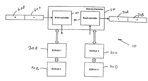
Referring first to Figure l, a block diagram of
memory system 10 for networking applications using RDRAM
modules 20A, 20B, 20C, 20D is illustrated. The memory
system 10 has a memory controller 30 within which resides
a write controller 40 and a read controller 50.
The system 10 works as follows. Data segments
3o 60A, 60B with a fixed size are received by the memory
controller 30 for buffering. These segments 60A and 60B,
are data transmission units that encapsulate data for
transfer between two points. After the segments 60A and
7
CA 02358332 2001-10-05
60B are received, the write controller 40 stores them by
writing them in one or more of the RDRAM modules 20A, 20B,
20C, 20D. Each RDRAM module 20A, 20B, 20C, 20D has
multiple memory banks and it is in these memory banks that
the segments 60A, 60B are stored.
When buffered segments are to be retrieved, read
controller 50 reads the buffered segments from t:he RDRAM
modules 20A, 20B, 20C, 20D and transmits these retrieved
segments as fixed size segments 70A, 70B.
1o One issue with RDRAM modules is that, as noted
above, sense amplifiers are shared between memory banks.
These sense amplifiers are the route by which data is
written to and retrieved from rows and columns within a
memory bank. Because of the shared sense amplifiers and
other factors, a memory bank has to undergo a transition
between a read access memory operation and a write access
memory operation (read-to-write transition). Thus, there
is a period of time, albeit small, during which no memory
operation may be performed on the memory bank.
2o Another issue with RDRAM modules is, again,
caused by the shared sense amplifiers. A write-to-read
transition, that is a transition between a write memory
access operation to a read memory access operation,
prevents a read operation from being executed on the same
RDRAM module as the last write operation during the
transition.
A third problem arises due to row access times
of a memory bank. Once a memory bank is accessed, no
other rows in that bank or any banks adjacent to the
3o accessed bank, may be accessed for a specific time
interval (referred to as a "gap"). Thus, during this
interval, the accessed bank along with any adjacent banks,
is unavailable for memory operations.
8
CA 02358332 2001-10-05
To partially overcome the above problems, all
memory operations for the memory controller 30 follow a
set, repeating pattern. This pattern is that of a write
memory access operation followed by a read memory access
operation, and, finally a short period during which no
operations are executed. This gap period is inserted to
account for the read-to-write transition. Thus, a WRG
(write-read-gap) pattern can be repeated as required.
The WRG pattern accounts for the read to write
1o transition with the time gap in the pattern and the write
to read transition problem can be accounted for by having
two RDRAM modules on the same databus to the memory
controller. This way, when. one RDRAM module is
unavailable due to the write to read transition, the other
RDRAM module can be accessed.
The third problem. is more difficult tc overcome
due to the shared sense amplifiers. To further illustrate
the issue, Figure 2 illustrates a schematic timing diagram
of the WRG pattern and the transitions involved. In
2o Figure 2, time interval 80 is the time gap inserted in the
WRG pattern to account for the read-to-write transitions.
Time interval 90 is the time interval during which an
RDRAM module cannot be accessed due to a write-to-read
transition. As noted above, this can be overcome by
having two RDRAM modules as the same databus. Time
intervals 100A, 100B are the time intervals during which a
memory bank and memory banks adjacent to it, cannot be
accessed due to row access times. As can be seen in
Figure 2 during the time interval 100A due to write
operation Wl, read operations R1 and R2 and write
operations W2 cannot access memory banks adjacent to or
the same as the memory bank accessed by write operation
Wl. Similarly, with reference to time interval 100B, read
9
CA 02358332 2001-10-05
operation R1 constrains the memory banks on which write
operations W2 and W3 and read operation R2 can be
performed. It must be noted that time intervals 100A and
100B are separately provided only for illustration
purposes. It must also be noted that the WRG pattern in
Figure 2 can be optimized for transferring blocks of 32
bytes of data to and from an RDRAM memory subsystem.
To account for the conflicts explained above,
read and write addresses can be selected to minimize such
1o conflicts. This can be done because in networking
applications memory controllers usually have full freedom
in selecting write addresses. However, read addresses are
usually predetermined by other factors that are beyond the
control of memory controllers.
z5 Given the above constraints, predetermined read
addresses that conflict with a previously accessed read
address can be handled by merely delaying, for one WRG
block, the read operation which uses these predetermined
addresses. This means that a NOP (no operation) is
2o inserted in the read section of the WRG block containing
the read operation which uses the conflicting read
address. As an example, i.f the read operation in WRG
block A accesses memory bank BK, and if the read operation
in WRG block B which immediately succeeds WRG block A,
25 similarly accesses memory bank BK, then there is a bank
conflict. To avoid the conflict, a NOP is inserted in WRG
block B in place of its read operation. This now
displaced read operation is then passed on to WRG block C.
If WRG block C immediately succeeds WRG block B, then the
3o displaced read operation is thereby delayed by one WRG
block or one repetition or the WRG pattern. By delaying
the displaced read operation by one WRG block, the bank
conflict is avoided.
CA 02358332 2001-10-05
With regard to write addresses, because the
memory controller can choose write addresses, more options
for avoiding bank conflicts are available. The criteria
for selecting write addresses can be the following:
a) For each read operation accessing a read
address in a WRG block, the write address chosen
for the write operation must be in a different
RDRAM module than the read address. Thus, if,
in a specific WRG block, a read operation
accesses RDRAM module Rl, then the write
operation in the same WRG block must choose a
write address located in RDRAM module other than
RDRAM module R1.
b) The selected memory to be accessed by a
selected write address must not be th~~ same bank
accessed by an immediately preceding write
operation. Furthermore, this selected memory
bank accessed by the selected write address must
not be a memory bank which will be accessed by
2o an immediately succeeding read opera tion. Also,
this selected memory bank cannot be a memory
bank immediately adjacent a memory bank that has
been accessed by an immediately preceding write
operation. Lastly, the selected memory bank
cannot be adjacent to a memory bank that is to
be accessed by an immediately succeedv~ng read
operation.
Based on the above, if a number of memory banks
are arranged, in order, as:
then bank B is adjacent to both banks A and C. Similarly,
banks C and E are adjacent to bank D. However, bank B is
not adjacent to bank D. From this configuration, if a
11
CA 02358332 2001-10-05
read operation accesses bank B, then the immediately
preceding write operation and the immediately succeeding
write operation cannot select write addresses contained in
any of banks A, B, or C. From the explanation in a)
above, if the immediately preceding write operation was in
the same WRG block as the read operation, then that
immediately preceding write operation would havEe to select
a write address that is in a different RDRAM module. This
removes the problem of bank conflict. The immediately
1o succeeding write operation can then choose a write address
contained in either of banks D or E as these arE~ neither
adjacent to nor the same as the bank accessed by
immediately preceding read operation.
It should be noted that, since read addresses
are predetermined, it is a simple matter to determine an
immediately succeeding read address for the above process.
The final criteria to be used in selecting a
write address relates less to bank conflicts and more to
the efficient use of resources. After the two criteria
listed above have been met for selecting a bank for a
write address, the remaining write address candidates must
pass a final test. The selected write address must be in
a memory bank that has the most space available for data.
In other words, the least full memory bank that conforms
to the two criteria above must be the selected bank.
When using the criteria above, it has been found
that the write efficiency increases. Using 128 ~Ibit RDRAM
modules with a 16-dependent bank structure, write
addresses, selected using the above criteria are not
3o blocked by bank conflicts until occupancy of the modules
approaches 1000.
Another benefit of the above criteria is that
delay between memory operations is decreased. Since write
12
CA 02358332 2001-10-05
operations are constrained by future read operations,
because the write address required for the write operation
is dependent on the read address for the read operation,
the actual write address to the RDRAM module cannot be
determined until the next read request arrives from
outside the memory controller. There is, therefore.
delay between operations as the required addresses are
supplied to the operations at roughly the same time.
While the above method selects the write address
to and thereby increases the writing efficiency of the
system, read efficiency is not affected. To improve the
read efficiency, the memory controller must be allowed to
select read addresses. One method of doing this which
allows the memory controller independence from f=he read
address selection process is to reorder the read
operations. In doing so bank conflicts between read
addresses can be reduced by moving conflicting read
addresses so that the read operations using there read
addresses are not temporally adjacent one another.
2o To implement the reordering of read operations a
frame size of M read operations is defined among the
repetitions of the WRG pattern. The memory controller can
then reorder read operations within the given frame size
of M operations. Since this leads to M! possix>le
orderings of read operations, the computational complexity
of the system increases significantly as M incrE~ases. It
must be noted that a frame size of M read operations
encompasses M repetitions of the WRG pattern.
The problematical computational comple-x_ity can
3o be controlled by defining a window size W reads operations
within the frame of size M. A frame is then divided into
window sections of size W read operations with each window
section overlapping its immediately preceding and
13
CA 02358332 2001-10-05
immediately succeeding window sections. The memory
controller is only allowed to reorder read operations
within a given window section. To illustrate this, Figure
3 presents a schematic diagram of three read operations,
Ro, R1, R~ with two window sections Wo, W1 overlapping the
read operation R,. Clearly the window size in this example
is 2 while the overlap interval is 1 read opera=ion. From
this Figure, the memory controller can thus reo der read
operations Ro and R1 as these are both in window section
1o W0. Similarly, read operations R1, R, can be reordered as
they are both in window section W1. To continue with the
example, if it is assumed that read operation R~ is to
continue to avoid a conflict with a preceding read
operation, and if read operation R, conflicts with read
operation R~, then read operations R~ and R- can be
reordered in windcw section W, to remove this conflict
between read operations R~ and R, .
One possible issue with the above is t:he
unbounded nature of the reordering. A read operation may,
2o theoretically, be shuffled indefinitely and thereby avoid
being executed. To prevent this, an absolute frame size M
is imposed. Window sections are not allowed to extend
beyond the boundaries of th.e absolute frame size. This is
illustrated in Figure 4 where window sections W",__, W«_1 . Wa
decrease in size as one gets closer to the bounds of frame
size M. In such a scheme, the last window section will
always have a size equal to that of one read operation.
It should be noted that each read operation in
Figures 3 and 4 are understood to be part of a larger,
3o repeating WRG pattern. However, to simplify the Figures,
only the read operations were illustrated.
14