Note: Descriptions are shown in the official language in which they were submitted.
CA 02358405 2001-07-04
WO 00/40975 PCT/US99/30127
TEXT PROBE INTERFACE ASSEMBLY AND MANUFACTURE METHOD
FIELD OF THE INVENTION
The invention is directed to an electronic test probe interface assembly and
method of manufacture. In particular, the invention employs a plurality of
conducting
paths, a floppy substrate and a diaphragm to provide the interface assembly.
BACKGROUND OF THE INVENTION
Probe card assemblies are required in the testing of solid state electronic
devices (Die or Chip) at certain steps of their manufacturing cycle. The Probe
Card is
the electro-mechanical interface between the device being tested and the
system that
performs the electrical test.
Probe Cards have been designed and manufactured using a technology that has
essentially remained the same for over 25 years. This old manufacturing
technology
lacked any automation, heavily dependent on manual assembly. It is therefore
costly
and with low consistency between multiple probe cards that are supposed to be
identical.
The industry has been seeking advanced methods of manufacturing Probe
Cards for the last decade. There have been a few innovations that have given
higher
reliability, yet they have not been cost effective, and therefor have a poor
'cost of
ownership' for the end user.
This invention gives the technical and cost benefits sought by the electronic
device manufacturing industry. The manufacturing process is more automated,
using
computer generated design algorithms, laser machining and semiconductor 'thin
film
CA 02358405 2001-07-04
WO 00/40975 PCT/US99/30127
technology'. Multiple Probe Cards are identical, having the exacting
specifications
required by the end user.
SUMMARY OF THE INVENTION
An interface is provided between terminals on an integrated circuit testing
device and corresponding terminals on an integrated circuit to be tested. The
integrated circuit has a predetermined pattern of test access pads. The
combination
includes a printed circuit board, a first plurality of conducting paths on the
printed
circuit board having test device ends configured for contacting ones of the
terminals
on the integrated circuit testing device. A floppy substrate is included and a
second
plurality of conducting paths is formed on the floppy substrate wherein the
conducting
paths have printed circuit board ends disposed for contact with ones of the
opposing
ends of the first plurality of conducting paths. A self supporting diaphragm
is
included with a third plurality of conducting paths on the self supporting
diaphragm
having conducting path ends disposed for contact with ones of the ends of the
second
plurality of conducting paths. Probe members are provided which extend from
the self
supporting diaphragm in a pattern corresponding to the predetermined pattern
of test
access pads. The probe members are connected to ones of the third plurality of
conducting paths. Resilient means extends between the printed circuit board
and the
self supporting diaphragm.
In another aspect of the invention an interface apparatus is provided for
connecting a plurality of tester terminals on an integrated circuit tester to
an integrated
circuit device which has a plurality of test access pads arranged in a
predetermined
pattern. A printed circuit board has a plurality of circuit board conducting
paths
thereon adapted for electrical contact on one end with ones of the plurality
of tester
terminals. A probe support diaphragm is provided having a plurality of probe
support
conducting paths thereon which have inner conductor ends and outer conductor
ends.
A plurality of probes is mounted on the probe support diaphragm disposed in a
pattern
corresponding to the predetermined pattern of integrated circuit device test
access
pads. The probes are connected to ones of the plurality of probe support
conducting
path inner ends. Resilient means is attached to and extends between the
printed circuit
board and the probe support diaphragm. A floppy ring extends between the
printed
circuit board and the probe support diaphragm in parallel with the resilient
means. A
-2-
CA 02358405 2001-07-04
WO 00/40975 PCT/LJS99/30127
plurality of conducting paths is formed on the floppy ring in contact with and
extending between ones of the plurality of circuit board conducting paths and
ones of
the plurality of probe support conducting pads.
In yet another aspect of the invention an interface module is provided for
connecting a plurality of tester terminals on a microcircuit tester to a
plurality of
substantially coplanar microcircuit access pads in a predetermined pattern on
an
integrated circuit. The combination includes a printed circuit board, a
plurality of
conducting paths on the printed circuit board disposed for electrical contact
with ones
of the plurality of tester terminals and a frustum surface shaped flexible
membrane
having a base adjacent the printed circuit board and an opening opposite the
base.
Further a plurality of conducting paths is formed on the flexible membrane,
which
paths extend from adjacent the base to adjacent the opening opposite the base
and are
in electrical contact with ones of the plurality of conducting paths on the
printed
circuit board adjacent the base. A diaphragm has an outer edge and an interior
portion
and a plurality of conducting paths which are formed on the diaphragm and
which
extend from positions toward the outer edge to positions toward the interior
portion.
The conducting paths on the diaphragm are in electrical contact at the
positions toward
the outer edge with ones of the plurality of conducting paths on the flexible
membrane
adjacent the opening opposite the base. A plurality of electrical contacts
have tips
which extend from the diaphragm in a pattern corresponding to the micro-
circuit
access pad predetermined pattern and which are in electrical contact with ones
of the
plurality of conducting paths on the diaphragm at the positions toward the
interior
portion. Resilient means surrounds the diaphragm interior portion and is
attached to
and extends between the printed circuit board and the diaphragm. In this
fashion, the
resilient means deflects to provide coplanarity between the tips on the
plurality of
electrical contacts and the microcircuit access pads. Further, the diaphragm
itself
deflects to provide contact between ones of the tips and ones of the micro-
circuit
access pads when local departure from coplanarity in the tips and micro-
circuit access
pads occurs.
A method of fabricating an interface module is disclosed which provides signal
conducting paths between terminals on an integrated circuit testing device and
a
pattern of circuit access pads on an integrated circuit. The interface module
has a
printed circuit board providing contact with the terminals on the integrated
circuit
-3-
CA 02358405 2001-07-04
WO 00/40975 PCT/US99/30127
testing device and signal conducting paths thereon. The method includes the
steps of
forming a floppy ring shaped in the form of a surface of a frustum and
depositing
signal conducting paths on the floppy ring. Further, a planar self supporting
diaphragm plate is formed and hole location and laser drilling is performed to
provide
a pattern of holes in the diaphragm plate in a pattern corresponding to the
pattern of
circuit access pads. Also included is the step of depositing signal conducting
paths on
the diaphragm plate wherein each conducting path has one end terminating at
ones of
the pattern of laser drilled holes. Pad contacts are inserted into ones of the
pattern of
laser drilled holes and the floppy ring is placed between the printed circuit
board and
the self supporting diaphragm plate in position so that ones of the floppy
ring
conducting paths are connected between ones of the printed circuit board and
ones of
the diaphragm plate signal conducting paths. The self supporting diaphragm
plate is
resiliently secured in a substantially parallel plane relationship with the
printed circuit
board. The pad contacts are adjusted so that the tips thereof lie in a plane
substantially
parallel to the planar self supporting diaphragm plate.
In a further form of the invention an interface is provided for connecting
terminals on an integrated circuit tester with a predetermined pattern of
circuit access
pads on an integrated circuit wherein a printed circuit board has a base on a
frustum
shaped flexible substrate positioned adjacent thereto.
A self supporting diaphragm is positioned adjacent to and extends across an
end of the frustum opposite the base. Resilient means is connected to and
extends
between the printed circuit board and the self supporting diaphragm to
maintain a
substantially parallel planar relationship therebetween when the resilient
means is in
an unstressed condition. A plurality of probes is mounted in the self
supporting
diaphragm, which extend therefrom in a pattern corresponding to the
predetermined
pattern of circuit access pads. Conductive signal paths are on the printed
circuit board,
the frustum shaped flexible substrate and the self supporting diaphragm which
provide
communication between the integrated circuit tester terminals and the circuit
access
pads.
BRIEF DESCRIPTION OF THE DRAWINGS
Figure 1 is an exploded view of the integrated circuit tester interface of the
present invention.
_4_
CA 02358405 2001-07-04
WO 00/40975 PCT/US99/30127
Figure 2 is a section along the line 2-2 of Figure 1.
Figure 3 is a partial section of the left side of Figure 2.
Figure 4 is an alternative embodiment of the present invention as seen in
section through a central portion of the self supporting diaphragm.
Figures 5A-SI show steps in the process of obtaining holes in the self
supporting diaphragm and positioning of contact pins in the holes.
Figure 6 is a view along the line 6-6 of Figure 2.
Figure 7 is a view along the line 7-7 of Figure 2.
DESCRIPTION OF THE PREFERRED EMBODIMENTS
Interface modules for connecting the terminals on an integrated circuit
testing
device to specific pads on an integrated circuit fall into several groups. One
such
group has contacts for making electrical connection to the integrated circuit
access
pads with individually flexible contacts. Buckling beam contacts or
cantilevered arm
contacts exemplify such contacts. Another general group is that wherein all of
the
contacts for the integrated circuit access pads flex together. Interface
assemblies of
this latter type are exemplified by those having flexible membranes on which
the pad
contacting contacts are carned, which also require a backup support member for
the
membrane to provide sufficient strength in the membrane. Alternatively, when
rigid
type membranes with sufficient internal strength have been utilized, it is
generally
difficult to acquire a high density of probes in the rigid membrane due to the
difficulty
of forming holes therein at sufficiently close intervals to acquire a high
density of
probes and at the same time obtain probes having sufficient strength
characteristics to
provide for a sufficient number of repetitive test cycles.
Probe cards requiring a high density of probes for integrated circuit or
electric
circuit (the terms 'integrated' and 'electronic' are used interchangeably in
this
specification) testing are often manufactured by hand and the probes on the
cards must
be precisely positioned manually. Adjacent probes must be spaced a particular
distance apart to assure they will not electrically contact one another.
Further, the tips
of the probes must be in a common plane to assure that all the probes will
contact the
pads on the integrated circuits being tested simultaneously with substantially
identical
force on each pad. This assures good electrical contact and reliable testing.
Alternatively, if the probes engage the integrated circuit pads with excessive
force, the
-s-
CA 02358405 2001-07-04
WO 00/40975 PCT/US99/30127
pads, and therefore the integrated circuits, may be damaged. Additionally,
since the
probe cards of this type are fabricated manually, there is a high probability
that such
probe cards will not have identical or even similar characteristics. The cost
of such
cards is predictably high.
The probe card of the present invention is assembled more efficiently and the
probe contact positioning is obtained with a higher degree of accuracy due to
the
automated manner in which the probes are located and the higher density of
probes
achievable through the method of the present invention. Additionally, though
the
procedure places the probe tips in coplanar relationship, the probe card and
method of
manufacture relating to the present invention affords individual probe
displacement to
compensate for integrated circuit pad height (local) variation as well as
collective
probe tip planar adjustment to compensate for (general) variation between the
plane of
the integrated circuit access pads and the plane of the probe mounting
diaphragm of
the present invention.
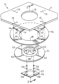
Refernng to Figure 1 of the drawings, an exploded view of a test probe
interface 10 of the present invention is shown having a printed circuit board
11 with
conductive signal paths 12 on the bottom surface thereof as shown, and having
ends of
the conductive paths extending toward the periphery of the printed circuit
board 11.
The peripheral ends of the conducting paths 12 are placed to contact terminals
on an
integrated circuit tester device (not shown). A hole 13 is shown centrally
located in
the printed circuit board 11 in this embodiment of the invention to provide
visibility
for ease of assembly.
The inner ends of the conducting paths 12 are configured to contact the ends
of
a plurality of conducting paths 14 located on a floppy ring 16 of thin
dielectric
material which has the shape of a surface on a frustum. The base of the
frustum is
adjacent the underside of the printed circuit board 11. The floppy ring is
fabricated of
some dielectric materials such as polyimide. The conductive paths 14 on the
floppy
ring 16 are seen to be formed on the upper side of the ring 16 from the outer
periphery
thereof to a point midway through the radial width of the ring. The paths 14
are there
led through vial 17 to the underside of the ring 16 (Figure 1) toward the
inner edge of
an opening 18 in the frustum opposite from the base of the frustum. The
conducting
paths 14 on the underside (Figure 1 ) of the floppy ring 16 are configured to
contact
conducting paths 22 on a self supporting diaphragm 21 at an outer end of the
_6_
CA 02358405 2001-07-04
WO 00/40975 PCT/IJS99/30127
conducting paths 22. The conducting paths 22 proceed toward an interior
portion of
the self supporting diaphragm 21 and terminate at through drilled holes 23.
The
drilled holes 23 are small in diameter, approximately .002 to .003 inches, and
are
formed in a manner and are shaped as will be hereinafter described. A needle
type
contact 24 is shown in Figure 1, which is set in each of the holes 23 in
electrical
contact with the conductive paths 22. The needle contacts 24 are preferably
fabricated
from tungsten or copper wire. The needles 24 in Figure 1 function as contact
probes
and are disposed in the self supporting diaphragm 21 in a pattern which
corresponds to
a pattern of circuit access pads 26 seen on an integrated circuit chip 27 to
be tested.
The integrated circuit itself is represented in Figure 1 by the enclosed
dashed lines 25.
An elastomer ring 28 is shown lying on the upper surface of self supporting
diaphragm
21 in Figure 1. The elastomer ring 28 adheres to the surface of self
supporting
diaphragm 21 on which it lies as well as to the undersurface of the printed
circuit
board 11 which it contacts inside the diameter of the central hole 18 in the
floppy ring
16. The elastomer ring is preferably Dow Corning 100% Silicone.
Figure 2 shows a section through the assembly of Figure 1 wherein the vertical
dimensions as seen in Figure 2 are slightly enlarged for purposes of clarity
and to add
some probe contacts24 as they would appear to address the pattern of circuit
access
pads seen in Figure 7. The test probe interface 10 is seen having the printed
circuit
board 11 with the signal conducting paths 12 formed on the underside thereof.
The
frustum substrate or conical ring 16 is shown having signal conducting paths
14
thereon with an upper end in contact with the signal conducting paths 12 on
the
printed circuit board and a lower end being in electrical contact with the
outer end of
signal conducting path 22 on the self supporting diaphragm 21. Figure 2 shows
the
vias 17 that allow the signal conducting paths 14 to migrate from the upper
side of the
frustum or floppy ring 16 to the underside thereof to thereby provide the
aforementioned electrical contact with signal paths 12 and 22. The self
supporting
diaphragm 21 is shown attached to the underside of the printed circuit board
11 by the
resilient ring 28. The frustum is shaped to maintain contact between the ends
of the
conducting paths 14 and 12 and 14 and 22 as pressure is exerted against the
base of the
frustum and the periphery of the hole 18 therein which lies opposite the base.
The
pressure is maintained by an appropriate spacing between the lower surface of
the
printed circuit board 11 and the upper surface of the self supported diaphragm
21.
CA 02358405 2001-07-04
WO 00/40975 PCT/US99/30127
Alternatively, the ends of the conducting paths 14 and 12 and 14 and 22 are
held in
contact using solder or conductive epoxy, such as electronics grade silver or
gold-
filled epoxy. The spacing between board 11 and diaphragm 21 is maintained by
the
resilient ring 28 and care is taken to maintain the board 11 and the diaphragm
21
within parallel planes at assembly. It may be seen in Figure 2 from the cross
section
of the resilient ring that the greatest dimension thereof extends between the
lower
surface of the printed circuit board 1 l and the upper surface of the self
supported
diaphragm 21. The holes 23 are prepared as will be hereinafter explained and
the
needle type probe contacts 24 are fixed therein in electrical contact with the
signal
conducting paths 22 on the upper surface of the diaphragm 21. The tips of the
probe
contacts 24 are placed in coplanar relationship through a process to be
hereinafter
described and are therefore available in a pattern corresponding to the
pattern of the
circuit access pads 26 surrounding the integrated circuit 25 on the
semiconductor
device 27. It is seen from the foregoing that the resilient means 28 will
deflect to
provide a generally coplanar relationship between the plurality of tips on the
electrical
contacts 24 and the plurality of microcircuit access pads 26. In addition, the
self
supporting diaphragm 21 is configured to deflect to provide contact between
each of
the tips on the plurality of probes 24 and corresponding ones of the
microcircuit access
pads 26. This feature comes into operation when local departure from a common
plane occurs between the contact probe tips and the microcircuit access pads.
The partial section of Figure 3 is closer to actual component part magnitudes
than is the depiction of Figure 2. The printed circuit board 11 is shown with
the
underside signal conducting paths 12 in contact with the signal conducting
paths 14 on
the floppy ring 16 which appears as a frustum in this embodiment. Contact is
shown
between the signal conducting path 14 and the conducting path 22 formed on the
surface of the self supporting diaphragm 21. The probe contact or needle 24 is
shown
in Figure 3 disposed at an angle to vertical in the depiction of Figure 3 for
the purpose
of providing rubbing between the contact tips and the access pads when contact
is
made with the circuit access pads 26 on the integrated circuit 27. The rubbing
results
from an overdrive between the tips and pads of up to 0.004 inches when the
probes are
positioned on the pads. The elastomeric ring 28 is shown in place in Figure 3
to
maintain the spacing between the board 11 and the diaphragm 21 and to also
maintain
the two elements in parallel planes. The resilient member 28,after being
stressed, will
_g_
CA 02358405 2001-07-04
WO 00/40975 PCT/US99/30127
return the printed circuit board 11 and the self supported diaphragm 21 to
their
assembled parallel plane positions. The floppy ring 16 is, in the best mode
known to
the inventors, thin polyimide with an electroplated metal signal conducting
path
pattern represented by the conducting paths 14 in the drawings. The self
supporting
diaphragm 21 is made of materials exhibiting high tensile strength, electrical
insulation properties and low thermal expansion characteristics. Materials
such as
quartz and certain plastics fall within this category. The self supporting
diaphragm is
in the form of a disk or rectangle, according to the application, and has a
certain
elasticity which allows individual ones of the mounted contact probes to be
moved
slightly against the elastic resistance of the diaphragm when the probes are
brought
into contact with circuit access pads 26. On the other hand, the entire
pattern of tips
on the probe contacts 24 s allowed to be moved into coplanarity with the
pattern of
integrated circuit access pads 26 against the resilient force afforded by the
resilient
member 28. Quartz is a preferred material for the self supporting diaphragm 21
and
has been used in thicknesses of .015 to .020 inches. Quartz also has
appropriate
dielectric properties, elasticity and tensile strength as well as a very low
coefficient of
expansion over a broad temperature range from cryogenic temperatures to
elevated
temperatures. Further, as will hereinafter be explained, quartz substrates can
be
manufactured to precise tolerances required in test probe interface
assemblies. The
assembly provided herein and illustrated in Figures 1 through 3 provides
uniform
"balanced contact force" at each probe tip. This means that each probe tip in
the array
of contact probes 14 contacts the integrated circuit access pads 26 with
substantially
equal amounts of probe pressure. The contact probes 24 have been found to
perform
well over repeated contact cycles when fabricated from the aforesaid tungsten
or
copper materials, because each material has excellent electrical conductivity
and
abrasive wear resistance.
Looking now at Figure 4 of the drawings, an alternative embodiment of the
present invention is shown. The self supporting diaphragm 21 is shown having
holes
23 therethrough and contacts 24 mounted therein in electrical contact with
signal
conducting paths 22 as described hereinbefore. A dielectric film 29 is
deposited on
top of the self supported diaphragm 21 and the signal conducting paths 22. The
dielectric film may be vapor deposited silicon nitride or a polysilicon
dielectric. An
electrically conducting ground plane 31 is deposited on top of the dielectric
layer 29.
-9-
CA 02358405 2001-07-04
WO 00/40975 PCT/US99/30127
An additional upper diaphragm layer 32 is fixed to the exposed surface of the
ground
plane 31. Holes 33 are drilled through the combination of layers just
described in
conjunction with this Figure 4 and the holes are plated. Additional probe
contacts 34
are placed in the holes 33, electrically fastened therein and overlayed with
additional
upper signal conducting paths 36. In this fashion, the impedance of the
conducting
paths 22 is controlled by the thickness of the dielectric layer 29 which
separates the
signal conducting paths 22 from the ground plane 31. Additionally, other
patterns of
signal conducting paths 36 are formed on the self supporting diaphragm
assembly
including diaphragm 21 and additional support member 32 so that additional
probe
contacts 34 may be added to the test probe interface assembly to contact
additional
access pads 26 for the integrated circuit 27. It should also be noted that the
contact
probes might take on any pattern configuration, including patterns of contact
pads 26
wherein pads 26 may exist at the periphery of the integrated circuit 27 or at
any points
internally thereof. The assembly of Figure 4 functions as does the assembly
depicted
1 S by Figures 2 and 3.
Looking at Figure SA, a self supporting diaphragm substrate 21 is shown,
which as has been mentioned hereinbefore, is a quartz material in a preferred
embodiment. As seen in Figure SB, the hole 23 in the diaphragm 21 has a
conical
shape. The hole 23 is formed by using a low power carbon dioxide laser to
drill
through the diaphragm. This laser drilling produces holes 23, which range from
.003
to .002 inches in diameter. The laser beam is optically focused and located
and the
lower power beam is able to drill holes having such small diameters because of
its
smaller beam diameter. It should be noted that an excimer laser works so well
on
Ultem 1000 TM material manufactured by Westlake Inc., which is a high
temperature
plastic and which is stable dimensionally over a relatively wide temperature
range.
The Ultem 1000 TM material has been used to make the diaphragm 21 for lesser
temperature and tolerance applications. For extremely wide temperature ranges,
however, the quartz material for the diaphragm 21 is preferred and the low
power
carbon dioxide laser is utilized for drilling holes 23. The quartz material
has been
empirically found to have an ideal modulus of elasticity, dielectric
properties and
temperature coefficient of expansion for the application described herein.
As seen in Figure SC the upper surface and the hole surfaces in the diaphragm
21 are coated with a copper layer 37. A contact probe such as the needle 24 is
inserted
- lo-
CA 02358405 2001-07-04
WO 00/40975 PCT/US99/30127
into the plated hole 23 as seen in Figure SD. The contact probe 24 is seen as
a conical
member in the figures having a wider apex angle than actually used for
purposes of
illustration. It should be noted that the contact probe 24 could be formed by
deposition of a conducting metal through the plated hole 23 to form the
contact probe.
Probes 24 in a finished state extend approximately .005 to .015 inches from
the lower
surface of the diaphragm 21. The contact probes are preferably in the range of
0.025
to 0.050 inches in overall length. The thickness of the quartz diaphragm
ranges from
0.015 to 0.020 inches in a preferred embodiment. The Ultem 1000TM material
will
vary in thickness from 0.020 to 0.040 inches while functioning as described
herein.
Unsupported smaller dimensions in the diaphragms, whether the diaphragm is a
circular disc or a rectangle, vary from approximately 2 to 5 inches.
An additional conducting layer 38 is deposited on top of the copper layer 37
as
seen in Figure SE. This layer 38 is in electrical contact with the probe
contact 24 and
secures the probe contact within the plated hole 23. A photoresist layer 39 is
deposited on top of the conducting layer 38 as seen in Figure SF. The
photoresist
layer 39 is partially removed to leave a pattern of photoresist on top of the
conducting
layer 38 which is representative of the pattern of signal conducting paths 22
to be
formed on the upper surface of the self supporting diaphragm 21. Copper layers
38
and 37 are etched away from the upper surface of diaphragm 21 except that
portion of
the two copper layers which underlie the pattern of photoresist 39 as seen in
Figure
SH. The pattern of conductive layers 38 and 37 remaining after the etch
represented in
Figure SH is the pattern of signal conducting paths 22 on the diaphragm 21.
When the
photoresist layer 39 is removed, the signal conducting path and probe contact
pattern
represented by the conducting paths 22 and the contact probes 24 remain on the
self
supporting diaphragm 21 as described hereinbefore and as shown in Figure SI.
A partial plan of the self supporting diaphragm 21 is shown in Figure 6
wherein a plurality of signal conducting paths 22 are shown terminated at
various
positions in the interior portion of the diaphragm. Probe contacts 24 extend
from the
lower surface of diaphragm 21 (not shown in Figure 7) the aforementioned
distance of
.005 to .015 inches. An integrated circuit device 27 is shown in Figure 7
having a
plurality of substantially coplanar circuit access pads 26 located on the
periphery of
the circuitry 25 as well as at various points within the interior of the
circuitry.
-11-
CA 02358405 2001-07-04
WO 00/40975 PCT/US99/30127
The depiction of Figure 6 shows a plurality of signal conducting paths 22
having ends within the interior of the self supporting diaphragm 21. The
contact
probes 24, formed by the contact needles shown in the figures, or by plated
through
contacts as mentioned hereinbefore, extend from the underside of the diaphragm
21 in
a pattern corresponding to the pattern of integrated circuit access pads 26
shown in
Figure 7. It may thus be seen that the invention described herein will provide
probe
contacts which may be brought to bear on any integrated circuit access pads 26
wherever they may lie throughout the surface of the integrated circuit 27. The
density
of the contact probes 24 is increased by the ability to drill very small holes
(.002 to
.003 inches diameter) in the self supporting substrate 21 on approximately
.004 inch
centers to receive probe contacts therein. The accuracy of hole location and
the
decrease in size of hole diameters provided by the laser drilling techniques
in materials
disclosed herein provide accurate high density probe contact patterns which
are
repeatable among test probe interface assemblies and which provide for proper
and
positive probe contact forces on each of the integrated circuit access pads in
a
predetermined pattern of access pads.
A method of fabricating an interface module is provided which affords signal
conducting paths between terminals on an integrated circuit testing device and
a
pattern of circuit access pads on an integrated circuit. The interface module
has a
printed circuit board that provides contact with the terminals on the
integrated circuit
testing device and further has signal conducting paths thereon. The method
includes
the steps of forming a floppy ring shaped in the form of a surface of a
frustum and
depositing signal conducting paths on the floppy ring. Further, the process
includes
the formation of a planar self supporting diaphragm plate. Laser location and
drilling
of a pattern of holes in the diaphragm plate follows, wherein the pattern of
holes
corresponds to the pattern of circuit access pads. The step of depositing
signal
conducting paths on the diaphragm plate wherein one end of each conducting
path
terminates at one of the holes in the pattern of laser drilled holes is
followed by
inserting pad contact probes into each of the holes in the pattern of laser
drilled holes.
Placing the floppy ring between the printed circuit board and the self
supporting
diaphragm plate, the floppy ring frustum is held therebetween by spacing the
printed
circuit board and the diaphragm plate to provide pressure between the
conducting
paths on the printed circuit board and the ends of conducting paths on the
floppy ring
-12-
CA 02358405 2001-07-04
WO 00/40975 PCT/US99/30127
at the base of the frustum as well as providing pressure between the
conducting paths
on the floppy ring at the opposing end of the frustum and conducting paths on
the
diaphragm plate. Alternatively, the conducting paths are connected with
conductive
epoxy, which in turn holds the floppy ring frustum in place. The printed
circuit board
and the self supporting diaphragm plate are fixed in this spaced condition in
parallel
planes by a resilient adhesive member disposed therebetween. The process
includes
the step of adjusting the tips of the pad contacts so that the tips lie in a
plane
substantially parallel t the plane of the diaphragm plate. The floppy ring 14
has
sometimes been called a flexible circuit interposer.
-13-