Note: Descriptions are shown in the official language in which they were submitted.
CA 02358660 2001-10-10
SERIAL COMMUNICATION DEVICE
AND
METHOD OF CARRYING OUT SERIAL COMMUNICATION
BACKGROUND OF THE INVENTION
FIELD OF THE INVENTION
The invention relates to a serial communication device and a method of
carrying out serial communication both used for confounding a memory in
duplex,
and more particularly to such a serial communication device and a method of
carrying out serial communication both presenting the same reliability as
reliability presented by a parallel bus.
DESCRIPTION OF THE RELATED ART
FIG. 1 is a block diagram of a conventional system for making
communication in duplex confounding.
The system is comprised of a first parallel bus controller 10, a second
parallel bus controller 12, a first buffer circuit lla associated with the
first
parallel bus controller 10 and electrically connected between the first and
second
parallel bus controllers 10 and 12, a second buffer circuit llb associated
with the
second parallel bus controller 12 and electrically connected between the first
buffer circuit lla and the second parallel bus controller 12, a 32-bit address
bus
13, a 32-bit data bus 14, and a 5-bit parity 15.
The 32-bit address bus 13, the 32-bit data bus 14 and the 5-bit parity 15
are all electrically connected between the first and second parallel bus
controllers
10 and 12 through the first and second buffer circuits lla and llb.
Communication in duplex confounding between the first and second
parallel bus controllers 10 and 12 is made through the 32-bit address bus 13
and
the 32-bit data bus 14.
Errors in parallel buses, that is, in the 32-bit address bus 13 and the
1
CA 02358660 2001-10-10
32-bit data bus 14 are detected through the 5-bit parity 15.
The above-mentioned conventional system illustrated in FIG. 1 is
accompanied with a problem that since the system has to include a lot of
signal
line for the parallel buses, the system unavoidably has a plurality of buffer
circuits 11a and 11b, resulting in much defectiveness in fabrication of the
system
and high cost for fabricating the system.
It would be possible to accomplish reduction in both cost and
defectiveness in fabrication of the system, if the parallel buses are replaced
with
serial buses. However, the use of serial bus causes another problem that bit
errors occur during communication, and hence, it is impossible to ensure the
same
reliability as reliability obtained when parallel buses are used.
Japanese Patent No. 2971006 (Japanese Unexamined Patent
Publication No. 8-265393) has suggested a method of carrying out serial
communication in a serial communication controller including at least one
first
buffer for receiving data and at least one second buffer for transmitting
data. In
the method, the first buffer is used for receiving data and the second buffer
is used
for transmitting data when data is received and transmitted in full-duplex
communication. The first and second buffers are used only for receiving data
when data is received in half-duplex communication. The first and second
buffers are used only for transmitting data when data is transmitted in half-
duplex communication.
However, the above-mentioned problems remain unsolved even in the
method suggested in the above-mentioned Publication.
SU_M__ARY OF THE INVENTInN
In view of the above-mentioned problems in the conventional system, it
is an object of the present invention to provide a serial communication device
and
a method of carrying out serial communication both of which are capable of
reducing the number of parts to thereby accomplish reduction in cost and
2
CA 02358660 2006-11-07
76319-8
defectiveness in fabrication, and providing the same
reliability as reliability obtained when parallel buses are
used, even though serial buses are used in place of parallel
buses.
In one aspect of the present invention, there is
provided a serial communication device bridging between an m
bit parallel bus and a serial bus, comprising: a parallel
bus interface circuit that receives as an input m bit wide
data from the parallel bus and multiplexes the m bit wide
data into sequentially generated n bit wide parallel data
segments, with n<m; a check bit producer that receives as an
input the n bit wide parallel data segments and produces as
an output a parallel arrangement of the n bit wide parallel
data segments and a generated error correcting code; and a
parallel-serial converter which converts said parallel
arrangement of the n bit wide parallel data segments and the
error correcting code from said check bit producer into
serial data.
There is still further provided a serial
communication device bridging between a parallel bus and a
serial bus, comprising: a serial-parallel converter which
converts serial data with an error correcting code
transmitted through said serial bus into parallel
arrangement of n bit wide parallel data segments and the
error correcting code; an error detector which checks the
error correcting code within said parallel data; and a
parallel bus interface circuit that demultiplexes the n bit
wide parallel data segments from the error detector into m
bit wide parallel data on the parallel bus.
There is further provided a serial communication
device bridging between a parallel bus and a serial bus,
comprising: a parallel bus interface circuit that receives
3
CA 02358660 2005-12-13
76319-8
as an input m bit wide data from the parallel bus and
multiplexes the m bit wide data into sequentially generated
n bit wide parallel data segments, with n<m; a check bit
producer that receives as an input the n bit wide parallel
data segments and produces as an output a parallel
arrangement of the n bit wide parallel data segments and a
generated error correcting code; a parallel-serial converter
which converts said parallel arrangement of the n bit wide
parallel data segments and the error correcting code from
said check bit producer into serial data; a serial-parallel
converter which converts serial data with an error
correcting code transmitted through said serial bus into
parallel arrangement of the n bit wide parallel data
segments and the error correcting code; and an error
detector which checks the error correcting code within said
parallel data; and wherein the parallel bus interface
circuit is also connected to receive as an input the
parallel data segments from the error detector, the parallel
bus interface circuit demultiplexing the n bit wide parallel
data segments from the error detector into m bit wide
parallel data on the parallel bus.
There is still further provided a method of
carrying out serial communication between a parallel bus and
a serial bus, comprising the steps of: multiplexing m bit
wide parallel data sequentially into n bit wide parallel
data segments, where n<m; applying an error correcting code
to each n bit wide parallel data segment; and converting
said parallel data with the error correcting code into
serial data.
There is also provided a method of carrying out
serial communication between a parallel bus and a serial
bus, comprising the steps of: converting serial data with
4
CA 02358660 2006-11-07
76319-8
an included error correcting code into parallel arrangement
of the n bit wide parallel data segments and the error
correcting code; checking the error correcting code applied
to each said parallel data segment; checking for an error
based on said error correcting code; and demultiplexing n
bit wide parallel data segments into m bit wide parallel
data on the parallel bus, wherein n<m.
There is additionally provided a method of
carrying out serial communication between a parallel bus and
a serial bus, comprising the steps of: when transferring
data from the parallel bus to the serial bus: multiplexing
m bit wide parallel data from the parallel bus into n bit
wide data segments, wherein n<m; applying an error
correcting code to each parallel data segment; and
converting each said parallel data segment with the error
correcting code into serial data; and when transferring data
from the serial bus to the parallel bus: converting serial
data with included error correcting codes transmitted
through said serial bus into parallel arrangement of the n
bit wide parallel data segments and the error correcting
code; checking the error correcting code applied to each
said parallel data segment; detecting an error in said error
correcting code; and demultiplexing the n bit wide parallel
data segments into m bit wide parallel data on the parallel
bus.
4a
CA 02358660 2004-08-06
76319-8
The advantages obtained by the aforementioned
present invention will be described hereinbelow.
In accordance with the present invention, the
number of parts for constituting the communication system
can be reduced to thereby accomplish reduction in cost and
defectiveness in fabrication of the communication system,
and the same reliability as reliability obtained when
parallel buses are used can be provided, even though serial
buses are used in place of parallel buses.
The above and other objects and advantageous
features of the present invention will be made apparent from
the following description made with reference to the
accompanying drawings, in which like reference characters
designate the same or similar parts throughout the drawings.
BRIEF DESCRIPTION OF THE DRAWINGS
FIG. 1 is a block diagram of a conventional system
for making communication in duplex confounding.
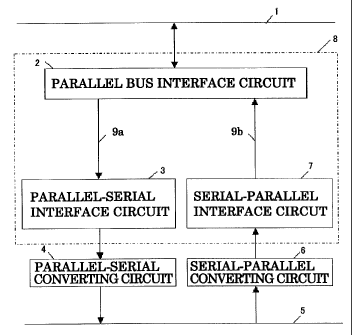
FIG. 2 is a block diagram of the serial
communication device in accordance with a preferred
embodiment of the present invention.
FIG. 3 is a time chart showing an operation of the
serial communication device illustrated in FIG. 1.
DESCRIPTION OF THE PREFERRED EMBODIMENTS
5
CA 02358660 2001-10-10
FIG. 2 is a block diagram of the serial communication device in
accordance with a preferred embodiment of the present invention.
The serial communication device is comprised of a bus bridge circuit 8
electrically connected to a parallel bus 1 including a 32-bit address bus and
a 32-
bit data bus, a parallel-serial converting circuit 4 electrically connected
between
the bus bridge circuit 8 and a serial bus 5, and a serial-parallel converting
circuit
6 electrically connected between the bus bridge circuit 8 and the serial bus
5.
The bus bridge circuit 8 is comprised of a parallel bus interface circuit 2
electrically connected to the parallel bus 1, a parallel-serial interface
circuit 3
electrically connected between the parallel bus interface circuit 2 and the
parallel-serial converting circuit 4, a serial-parallel interface circuit 7
electrically
connected between the parallel bus interface circuit 2 and the serial-parallel
converting circuit 6, a first 8-bit data-multiplexing bus 9a electrically
connecting
the parallel bus interface circuit 2 and the parallel-serial interface circuit
3 to
each other, and a second 8-bit data-multiplexing bus 9b electrically
connecting the
parallel bus interface circuit 2 and the serial-parallel interface circuit 7
to each
other.
The parallel and serial buses 1 and 5 may have any structure.
The parallel bus interface circuit 2 act as an interface to the parallel
bus 1. When data is transmitted to the serial bus 5 from the parallel bus 1,
the
parallel bus interface circuit 2 multiplexes 32-bit address, data and command
transmitted through the parallel bus 1, into 8-bit (1 byte) addresses, data
and
commands, and outputs the thus multiplexed addresses, data and commands to
the parallel-serial interface circuit 3 through the first 8-bit data-
multiplexing bus
9a. When data is transmitted to the parallel bus 1 from the serial bus 5, the
parallel bus interface circuit 2 transmits data multiplexed into 1-byte data,
to the
parallel bus 1 as 32-bit address, data and command.
The parallel-serial interface circuit 3 acts as an interface for
transmitting serial data, and produces a bit for checking an error correcting
code
6
CA 02358660 2001-10-10
in serial communication (hereinafter, such a bit is referred to as "ECC check
bit").
The parallel-serial interface circuit 3 receives address, data and command
byte by
byte from the parallel bus interface circuit 2, produces a ECC check bit on
receipt
of 1-byte of address, data and command, applies the thus produced ECC check
bit
to each 1-byte of address, data and command, and outputs each 1-byte of
address,
data and command with the associated ECC check bit, to the parallel-serial
converting circuit 4.
The parallel-serial converting circuit 4 receives the parallel data byte
by byte from the parallel-serial interface circuit 3, converts the received
parallel
data to serial data, and outputs the thus converted serial data to the serial
bus 5.
The serial-parallel converting circuit 6 receives serial data through the
serial bus 5, converts the received serial data to parallel data byte by byte,
and
outputs the thus converted parallel data to the serial-parallel interface
circuit 7.
The serial-parallel interface circuit 7 detects a ECC check bit, corrects
errors in error correcting codes, and acts as an interface for transmitting
parallel
data. Specifically, the serial-parallel interface circuit 7 checks ECC check
bits in
address, data and command to thereby detect errors in error correcting codes,
and
corrects the detected errors. Then, the serial-parallel interface circuit 7
converts
1-byte data transmitted from the serial-parallel converting circuit 6, into 32-
bit
address, data and command, and multiplexes the 32-bit address, data and
command into 8-bit (1 byte) addresses, data and commands, and outputs the thus
multiplexed addresses, data and commands to the parallel bus interface circuit
2
through the second 8-bit data-multiplexing bus 9b.
The serial-parallel interface circuit 7 checks the ECC check bits in
address, data and command to thereby detect errors in the error correcting
codes.
If the serial-parallel interface circuit 7 detects a 1-bit error in the error
correcting
codes, the serial-parallel interface circuit 7 corrects the detected 1-bit
error,
whereas if the serial-parallel interface circuit 7 detects a 2-bit error in
the error
correcting code, the serial-parallel interface circuit 7 abandons an access
7
CA 02358660 2001-10-10
associated the detected error.
FIG. 3 is a time chart showing a relation among addresses, data,
commands and ECC check bits.
Hereinbelow is explained an operation of the serial communication
device in accordance with the embodiment.
When data is transmitted to the serial bus 5 from the parallel bus 1, the
parallel bus interface circuit 2 multiplexes 32-bit address, data and command
transmitted through the parallel bus 1, into 8-bit (1 byte) addresses, data
and
commands, and outputs the thus multiplexed addresses, data and commands to
the parallel-serial interface circuit 3 through the first 8-bit data-
multiplexing bus
9a.
The parallel-serial interface circuit 3 receives address, data and
command byte by byte from the parallel bus interface circuit 2, produces a ECC
check bit on receipt of 1-byte of address, data and command, applies the thus
produced ECC check bit to each 1-byte of address, data and command, and
outputs each 1-byte of address, data and command with the associated ECC check
bit, to the parallel-serial converting circuit 4.
The parallel-serial converting circuit 4 receives the parallel data byte
by byte from the parallel-serial interface circuit 3, converts the received
parallel
data to serial data, and outputs the thus converted serial data to the serial
bus 5.
When data is transmitted to the parallel bus 1 from the serial bus 5,
address, data and command are transmitted to the serial-parallel converting
circuit 6 through the serial bus 5, and are converted into parallel data in 1-
byte in
the serial-parallel converting circuit 6. The thus converted 1-byte parallel
data
are transmitted to the serial-parallel interface circuit 7.
The serial-parallel interface circuit 7 converts the 1-byte serial data
transmitted from the serial-parallel converting circuit 6, into 32-bit
address, data
and command, and multiplexes the 32-bit address, data and command into 8-bit
(1 byte) addresses, data and commands, and outputs the thus multiplexed
8
CA 02358660 2001-10-10
addresses, data and commands to the parallel bus interface circuit 2 through
the
second 8-bit data-multiplexing bus 9b.
In addition, the serial-parallel interface circuit 7 checks the ECC check
bits in address, data and command to thereby detect errors in the error
correcting
codes. If the serial-parallel interface circuit 7 detects a 1-bit error in the
error
correcting codes, the serial-parallel interface circuit 7 corrects the
detected 1-bit
error. If the serial-parallel interface circuit 7 detects a 2-bit error in the
error
correcting code, the serial-parallel interface circuit 7 abandons an access
associated the detected error.
The 32-bit address, data and command are transmitted to the parallel
bus interface circuit 2 from the serial-parallel interface circuit 7, and
then,
transferred to the parallel bus 1 through the parallel bus interface circuit
2.
The parallel-serial interface circuit 3 produces the ECC check bits for
address, data and command, and applies the ECC check bits to each 1-byte of
address, data and command at timings illustrated in FIG. 3 in accordance with
clock pulses.
Similarly, the serial-parallel interface circuit 7 checks the ECC check
bits in address, data and command at timings illustrated in FIG. 3 in
accordance
with clock pulses.
While the present invention has been described in connection with
certain preferred embodiments, it is to be understood that the subject matter
encompassed by way of the present invention is not to be limited to those
specific
embodiments. On the contrary, it is intended for the subject matter of the
invention to include all alternatives, modifications and equivalents as can be
included within the spirit and scope of the following claims.
9