Note: Descriptions are shown in the official language in which they were submitted.
___ _ _. ___ ø_ Y 4~ .. __ ___ __ _ __
CA 02358709 2001-07-20
F iELD OF TIC INV~111TION
Th,e present iavention rela~ea to validatorsr and in
particular, relates to valic~ators having optical scanrlera
_ far measuring the reflectance of paper bankuoteB as they
move past a sensor.
~~xourr~ o~ z~ nvv~y i ioN
The evaluation of bar~cnotes to determine their
authenticity in theory is relatively straightfoZ~vaard,
rowever, in practice, it is quite difficult to carry out in
a cost effective manner. Banknotes are evalu$ted by
scanning stripped regions of the dote or security paper
as it is icoved past a sensor. The banknote is normally
evaluated wits respect to optical characteristics, magr~etiC
characts~=istics and/or with respect to capacitance.
Published Application GB 2093179A discloses a
system fnr measuring the opacity of ba~2k_'rlotes anal detecting
poles in banknotes. A rads.ation source is provided on one
side of the bar_knote and two receivers are provided on the
oppos:~te side of the banknote. This arrangement allows
independent detection of izoles or tears as well as a
measurement of opacity.
U.S. Patent 5,304,813 discloses an arrangement for
optically sensing characteristics of banknotes using a
series of radiation emitters, spaced either site of a
photoelectric element and having a particular angular
relationship there~rith.
The optical characteristics of a banknote are
evah_ated by measuring the amot;nt of radiation reflected
from the banknote. The optical sensors include erdtters
which produce radiation of different wave lengths, and
focus the radiation or_ a particular target location of the
barll~.ote. The reflected radiation is measured and compared
1 -
Printed:l2-01-2001 ' 1
CA 02358709 2001-07-20
wi~?rence s'_gnal$ to determine whether to accept or
reject the banknote.
This optical evaluation ie difficult in that the
exact spacing of the bat~ote grcun the optical sensor
varies as the banknote ie, ess~tially, f7.oatit~g ~rithin an
oversized pathway along which the bss~ote moves. In
addition, the bsnJaiace Can be angled in the pathway
lorgitudianlly and laterally, even though the banla~ote is
generally centered. Thug, the spacing sad the angle
change, which influences the measured signal. Furthermore.
czeases in the banknote also caussa angle variations which
in turn ir.~pect the amount of radi ation that will be
reflected from the b~ote back to a sensor. Other
factors which affect the measured signal include the t~mount
of radiation reflected back to a receiver by the optical
sensor which radiation has not been r~flected by~the
banJoZOte. This portion of the signal typically produces
what is referred to as cross-talk and it is desirable to
keep this to as small a level as possible.
The pathway typically includes additiarml elements
or surfaces between the optical sensor and the banknote and
these elements ar s~.xrfaces ca:~ cause reflected radiation.
which again is not dependent upon the banknote. For
example, there coul3 be a window member which forms part of
the pathway with the optical sensor directly behind the
window. The window provides the desired smooth pathway.
but increases cross--talk.
ether optical ban3rnote scaru~l~.ng arra.~gernents have
positianed the emitter at a first acute ar_g3e, relative to
the banknote, and appropriately positioned the receiver at
a different angle for receiving the reflected radiation.
Two distinc= optical arrangements are provided to focus the
emitted ana received radiation. Unfortunately, these
systems produce significant variations with respect to
- 2 --
Printed:l 2-01-2001;
CA 02358709 2001-07-20
~ta~3.cas in the position of the ban'~ota in the pathway
as well as variatiory.s due to creaewa in the be~nlaxot~ .
3'he preseat inv~tiart provides an optical sensor
with improved accuracy in the measurement of the optical
_ reflecting properties of a banknote 8s the ban3caote is
moved past the sensor.
sub or rxx znw~mmzo~
A validator according to the present invention
comprises a pathway through which the bar~a~ote is moved cad
an optical sensor ~.s positioned in this pathway for
evaluating the o~rtical characteristics on a face of the
banknote. The optical sexi~or comprises a lens, a plurality
of radiation emitters and a radiat:Lor r~~~~= °r ~'"-e 'sr°
- 2a -
Printed:l2-01-2001 ;
CA 02358709 2001-07-20
WO 00/49582 PCT/CA99/00116
has a first surface which is generally planar and a second
surface which is convex. These surfaces cooperating to
define a focal point of the lens which faces the convex
surface. The pathway includes an opening which receives
the lens, with the planar surface of the lens closing the
opening and forming part of the pathway. The radiation
emitters and radiation receiver are closely clustered at
the focal point of the lens and include a shield member
which isolates the receiver from direct radiation of the
emitters. The lens collimates the emitted radiation of the
emitters to produce generally parallel rays of radiation
which are reflected by the banknote as it moves past the
sensor. The reflected radiation from the banknote that
impinges on the lens is focused by the lens and directed to
the receiver. The lens directs radiation reflected by the
convex surface and the planar surface of the lens away from
the receiver and reduces cross-talk between the receiver
and the emitters.
According to a preferred aspect of the invention,
the emitters each emit radiation of a different wavelength.
According to a further aspect of the invention, the
emitters are clustered together with minimal spacing
therebetween.
According to yet a further aspect of the invention,
the emitters and the receiver are separated by a screening
member.
According to yet a further aspect of the invention,
the emitters and the receiver are all located on a common
circuit board.
According to yet a further aspect of the invention,
the emitters include at least two different types of
emitters to produce radiation having two desired wave
lengths for investigating a banknote.
- 3 -
CA 02358709 2001-07-20
WO 00/49582 PCT/CA99/00116
According to yet a further aspect of the invention,
five emitters are provided, each of which produce a wave
length of a different radiation for investigating the
banknote.
BRIEF DESCRIPTION OF THE DRAWINGS
Preferred embodiments of the invention are shown in
the drawings, wherein:
Figure 1 is an illustrative view of part of a
validator showing a banknote moving past an optical sensor;
Figure 2 is a top view of the optoelectronic
components of the optical sensor;
Figure 3 is a sectional view taken along AA of
Figure 2; and
Figure 4 is an illustrative view showing the
positioning of the emitters and receivers to reduce cross-
talk.
DETAILED DESCRIPTION OF THE PREFERRED EMBODIMENTS
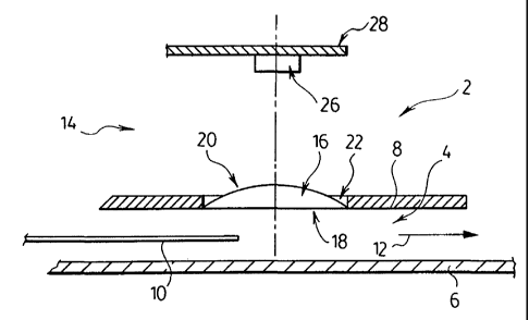
The validator 2 includes a pathway 4 for moving the
banknote 10 past an optical sensor 14. The pathway
includes an exterior wall 6 and an interior wall 8 having a
port 22 in the interior wall 8. The optical sensor 14
includes a lens 16 which is sized to fit into the port 22
as generally shown in Figure 1. The lens 16 includes a
planar surface 18 which forms a continuation of the
interior wall 8 of the pathway and effectively closes the
port 22. The lens also includes a convex surface 20 which
faces the opto-electronic components 26. The lens is
preferrably, an aspherical lens.
The lens cooperates with the opto-electronic
component 26 secured on the circuit board 28. The opto-
electronic component includes a series of pins soldered to
the circuit board.
- 4 -
CA 02358709 2001-07-20
WO 00/49582 PCT/CA99/00116
Details of the opto-electronic component 26 and its
relationship with lens 16 are shown in Figures 2 and 3.
Five emitters 30 are placed in a cluster type arrangement
on the support 27 such that the spacing between emitters is
quite small. The emitters are non-directional and
preferably emit radiation of different wave lengths for
evaluating the reflecting properties of the banknote as it
moves past the sensor. A receiver 32 is also positioned on
the support 27 and is separated from the emitters 30 by
means of the spacer or barrier 34 which shields the
receiver 32 from direct radiation of the emitters 30. The
receiver 32 is positioned in close proximity to the
emitters and slightly offset from the focal point.
The optical properties of the sensing arrangement
are shown in additional detail in Figure 4. The emitters
30 are located at the focus of the lens and produce
radiation. Most of the radiation is transmitted through
the lens and forms a collimated beam for radiating a strip
of the banknote as it moves past the sensor. The radiation
reflected by the banknote that impinges on the lens is
redirected and focused on the receiver 32. Variation of
the spacing of the banknote from the lens does not
appreciably effect the results, as the radiation has been
collimated and is in parallel rays. The slight offset in
the position of the receiver relative to the focal point is
not significant.
The radiation reflected by the lens indicated by
reflected beams 38, 40, 42 and 44 and if received
contributes to undesirable cross talk. Beams 38 and 40
strike the convex surface 20 of the lens and are reflected
by the surface. Most of the radiation will pass through
the lens for irradiating the banknote, but there is a
portion of the radiation that will be reflected. The
convex nature of the lens directs this radiation outwardly
and away from the receiver 32. In this way, reflected
radiation from the aspherical surface 20 of the lens is
- 5 -
CA 02358709 2001-07-20
WO 00/49582 PCT/CA99/00116
directed outwardly and the effect on the signal received by
the receiver 32 is minimal.
Reflected radiation 42 and 44 is produced due to
radiation which passes through the first surface of the
lens and is reflected by the planar surface 18 of the lens.
This reflected radiation is focused at point 50 located to
one side of the receiver 32. In this way, reflected
radiation returned by the planar surface 18 is focused at a
point exterior to one side of the receiver and thus the
effect of such reflected radiation on the receiver is
reduced.
Conveniently, the opto-reciever 32 and the emitters
30 are all produced on a common support and the position
thereof is accurately determined. The aspherical lens 16
appropriately processes the emitted radiation to produce a
collimated beam for radiating the banknote, and the
reflected radiation from the banknote is focused and
directed to the receiver 32 closely positioned at the focal
point of the lens. With this arrangement, the signal
produced by the opto-receiver more closely correlates with
the optical properties of the scanned banknote.
The present optical arrangement, has been designed
to accept that wobble of the banknote within the pathway
cannot be eliminated and as such the separation distance of
the banknote from the optical sensor will vary. The effect
of this varying distance has been reduced, due to using a
collimated beam of radiation for exposing the banknote.
The structure also positions a planar surface of the
optical lens to form a continuation of the pathway wall,
and as such, additional optical members are eliminated.
The lens has been designed to cause a large portion of any
radiation reflected by the lens itself to be directed away
from the receiver, or be focused at a point to one side of
the receiver. In this way, measured radiation reflected by
- 6 -
CA 02358709 2001-07-20
WO 00/49582 PCT/CA99/00116
the lens is reduced and is generally the same for the
radiation at different wave lengths.
This structure also uses a plurality of non-
directional emitters for producing radiation of several
different wave lengths. These wave lengths are selected to
reveal certain inks used in fraudulent banknotes.
Preferably, three of the emitters emit radiation in the
visible range and two of the emitters emit radiation in the
infrared range.
The present structure has resulted in improved
accuracy of the scanning of the banknote and a simplified
system.
With the present invention, a very simple
construction for an optical sensor is realized. The lens
is designed to act as a plug for the aperture in the
pathway, and therefore, the lens acts to appropriately
process the radiation, and as a window for the pathway.
The flat surface of the lens forms a continuation of the
walls of the pathway and does not change the position of
the banknote as it moves past the optical sensor. The
interior surface of the lens is made aspherical
(hyperboloid-like). This shape reduces cross-talk between
the emitters and the receiver. Basically, the radiation
reflected by the flat surface of the lens is generally
directed away from the receiver. In the present structure,
the plurality of light emitters and the photo-detector are
located in immediate proximity to the centreline of the
lens and adjacent the focus of the lens. The radiation
from the emitters form a collimated beam irradiating a
banknote, and reflected radiation from the banknote is
generally directed to the photo-detector. A further aspect
of the structure is the flat surface of the lens which is
used to close the port in the pathway. This reduces cross-
talk by simplifying the optical path and reducing the
amount of radiation that will be reflected. The plurality
CA 02358709 2001-07-20
, o rs are located as close together as possi?ale.
Thal~ aroupirig. or alueterir~g of the s~ittar~, preferably
produces signals of diffe-ent wave langrthe which ars
ess~tially equau.Iy effaczed by the proaertiee of tho
optical system. In this way, the measured eier~al more
accurately corresponc4a to the actual properties of the
banlaao t a .
_ g _
TDThL F. ~9
Printed:12-01-2001 ~ 4