Note: Descriptions are shown in the official language in which they were submitted.
CA 02358835 2001-10-16
TITLE OF THE INVENT7:ON
SNUBBER CIRCUIT AND POWER TRANSFORMER USING THE SAME
BACKGROUND OF THE INVE1NTION
[Field of the Invention]
The present invention relates to a snubber circuit
for suppressing a voltage ringing at a time of a turn-off
of a switch element and a power transformer such as a
switching power supply, using the snubber circuit.
[Description of the Related Art]
Examples of power transformers include switching
power supplies of both insulated types using a converter
transformer and non-insulated types using no converter
transformer.
In both types of switching power' supplies, a switch
element experiences sudden voltage changes (a voltage
ringing phenomenon) at a time of a turn-off of the switch
element due to a leakage inductance o;f a choke coil or a
primary coil of the converter transformer.
A snubber circuit is provided for' mainly suppressing
the voltage ringing.
The voltage ringing at the time of the turn-off of
the switch element is especially large if the switching
power supply has the large leakage inductance in the primary
coil of the converter transformer. Therefore, it is
preferred that the snubber circuit can suppress the voltage
ringing more efficiently.
However, when the leakage inductance is large,
suppressing voltage ringing with a conventional snubber
circuit has resulted in huge power loss.
1
CA 02358835 2001-10-16
SUMMARY OF THE INVENTION
Accordingly, a primary object of the invention is to
provide a snubber circuit capable of efficiently
suppressing a voltage ringing at a time of a turn-off of
a switch element while keeping an energy loss to a
sufficiently low level.
Other objects, features, and advantages of the
invention would be obvious from the following description.
The present invention is, in summary, a snubber
circuit provided in a power transformer including at least:
a switch element for operating for a power transformation
control; a magnetic substance for a storing and releasing
energy in relation to power transformation accompanying
with an operation of the switch element;; and a commutating
diode for conducting by means of the energy stored in the
magnetic substance, the snubber circuiit including: a first
series circuit composed of a capacitor and a diode connected
in series; and a second series circuit composed of a coil
and a diode connected in series, wherein the first series
circuit is connected in parallel with the commutating diode
in a state that the capacitor is connected to the magnetic
substance side in the commutating diode; and the second
series circuit is connected between a connecting portion
between the capacitor and the diode i,n the first series
circuit and a commutating diode non-connecting side in the
magnetic substance.
The power transformers mentioneii above include not
only switching power supplies , but also other kinds of power
transformers such as inverters.
The switch elements include not only switching
transistors such as bipolar transistors and MOS transistors,
but also other kinds of switch elements.
2
CA 02358835 2001-10-16
The magnetic substance mentions;d above include any
magnetic substance such as a secondary coil of a transformer,
a choke coil and other magnetic components, which stores
and releases energy as a result of operation of a switch
element.
The commutating diodes include diodes which conduct
by means of stored energy of a magnEaic substance, for
example, a rectifying diode disposed i:n the secondary side
of a transformer in a flyback switching power supply and
a commutating diode in the secondary s:i.de of a transformer
in a forward switching power supply.
In the first series circuit, the capacitor and the
diode include any aspects connected in series whether
directly or indirectly.
An aspect in which the first series circuit is
connected to the commutating diode in parallel includes any
aspects connected in parallel whether directly or
indirectly.
An aspect in which the capacitor within the first
series circuit is connected to the magnetic substance
connecting side in the commutating diode includes any
aspects connected to either an anode side or cathode side
of the commutating diode whether directly or indirectly.
A connecting portion of a capacitor and a diode in
the first series circuit includes any aspects in which the
capacitor and the diode connected whether directly or
indirectly.
In the second series circuit , the coil and the diode
include any aspects connected in series whether directly
or indirectly.
An aspect in which the second series circuit is
connected to a commutating diode non-corinecting side in the
3
CA 02358835 2001-10-16
magnetic substance includes any aspects connected to the
commutating diode non-connecting side of the magnetic
substance whether directly or indirectly.
In accordance With the snubber circuit of the
invention, in a state that the energy is fully stored in
the capacitor of the first series circuit, when the switch
element is turned off, since the stored energy of the
capacitor is released through the magnetic substance, an
electric current of the switch element doesn't rapidly
become smaller, but gradually becomes smaller.
Consequently, the voltage ringing at a time of a
turn-off of the switch element is suppressed.
In this case, even if the coil used for power
transformation in a switching power supply employing a
converter transformer, the switching power supply
employing a tapped inductor and the like has a large leakage
inductance, since a component is formed by a capacitor,
diode and coil, enhancing voltage ringing suppression
effects does not cause power loss.
As mentioned above, according to the invention, the
voltage ringing at the time of the turn-off of the switch
element can be suppressed while consiiierably suppressing
the power loss.
A power transformer in accordance With the invention,
includes: a switch element for operating for a power
transformation control; a magnetic substance for storing
and releasing an electrical energy in relation to the power
transformation that accompanies operation of the switch
element; a commutating diode for conducting by means of the
stored energy of the magnetic substance; and a snubber
circuit for suppressing voltage variations at a time of a
turn-off of the switch element, wherein the snubber circuit
4
' CA 02358835 2001-10-16
has a first series circuit of a capacitor and a diode and
a second series circuit of a coil and a diode, the first
series circuit is connected in parallel to the commutating
diode in a state that the capacitor' is connected to a
magnetic substance connecting side in the commutating diode,
and the second series circuit is connected between a
connecting portion of the capacitor and the diode in the
first series circuit and a commutating diode non-connecting
side in the magnetic substance.
According to the power transformer a.n accordance with
the invention, since the snubber circuit is used, a
suppression of the voltage ringing .at the time of the
turn-off of the switch element and a power loss accompanying
the suppression thereof can be considerably reduced.
BRIEF DESCRIPTION OF THE DRAWINGS
These and other objects as well as advantages of the
invention will become clear by the fo:Llowing description
of preferred embodiments of the invention with reference
to the accompanying drawings, wherein:
Fig. 1 is a circuit diagram shotaing a main part of
a switching power supply in accordance with a preferred
embodiment of the invention;
Fig. 2A is a voltage waveform d'.iagram of a switch
element SW1 in the switching power supF>ly shown in Fig. 1;
Fig. 2B a.s a current waveform diagram of the switch
element SWl in the switching power supply shown in Fig. 1;
Fig. 2C is a current waveform diagram of a rectifying
diode D1 in the switching power supply shown in Fig. 1;
Fig. 2D is a current waveform diag:cam of a eommutating
diode D2 in the switching power supply in Fig. l;
Fig. 3 is a circuit diagram shoviing a main part of
5
CA 02358835 2001-10-16
a switching power supply being subjected to a description
of a current behavior in each portion;
Fig. 4 is a circuit diagram showing a major part of
a switching power supply being sub jected to a description
of a current behavior in each portion;
Fig. 5 is a circuit diagram showing a major part of
a switching power supply being subjected to a description
of a current behavior in each portion;
Fig. 6 is a circuit diagram showing a major part of
a switching power supply being subjected to a description
of a current behavior in each portion;
Fig. 7 is a circuit diagram showing a major part of
a switching power supply being subject:ed to a description
of a current behavior in each portion;
Fig. 8 is a circuit diagram showing a major part of
a switching power supply being subjected to a description
of a current behavior in each portion;
Fig. 9 a.s a circuit diagram showing a major part of
a switching power supply being subject:ed to a description
of a current behavior in each portion;
Fig. 10A is a voltage waveform diagram of a switch
element SW1 shown in Figs. 3 to 9;
Fig. lOB is a current waveform diagram of the switch
element SWl shown in Figs. 3 to 9;
Fig. lOC is a current waveform diagram of a
commutating diode D2 shown in Figs. 3. to 9;
Fig. lOD is a current waveform diagram of a capacitor
C3 shown in Figs. 3 to 9;
Fig. 10E is a voltage waveform diagram of the
capacitor C3 shown in Figs. 3 to 9;
Fig. lOF is a current waveform showing of a coil L2
shown in Figs. 3 to 9;
6
CA 02358835 2001-10-16
Fig. 11 is a circuit diagram showing a major part of
a switching power supply of another preferred embodiment
of the invention;
Fig. 12A is a voltage waveform diagram of a switch
element SW1 in the switching power supply shown in Fig. 11;
Fig. 12B is a current waveform diagram of the switch
element SW1 in the switching power supply shown in Fig. 11;
Fig. 12C is a current wavef:orm diagram of a
commutating diode D2 in the switchinf power supply shown
in Fig. 11;
Fig. 13 is a circuit diagram showing a major part of
a switching power supply being subjected to a description
of a current behavior in each portion;
Fig. 14 is a circuit diagram showing a major part of
a switching power supply being subjected to a description
of a current behavior in each portion;
Fig. 15 is a circuit diagram showing a major part of
a switching power supply being subjected to a description
of a current behavior in each portion;
Fig. 16 is a circuit diagram showing a major part of
a switching power supply being subjected to a description
of a current behavior in each portion;
Fig. 17 is a circuit diagram showing a major part of
a switching power supply being subjected to a description
of a current behavior in each portion;
Fig. 18 is a circuit diagram shoring a major part of
a switching power supply being sub jected to a description
of a current behavior in each portion;
Fig. 19 is a circuit diagram showing a major part of
a switching power supply being sub ject~ed to a description
of a current behavior in each portion;
Fig. 20A is a voltage waveform diagram of a switch
7
CA 02358835 2001-10-16
element SW1 shown in Figs. 13 to 19;
Fig. 20B is a current waveform diagram of the switch
element SWl shown in Figs. 13 to 19;
Fig. 20C is a current wave:Eorm diagram of a
commutating diode D2 shown in Figs. 13 to 19;
Fig. 20D is a current waveform diagram of a capacitor
C3 shown in Figs. 13 to 19;
Fig. 20E is a voltage waveform diagram of the
capacitor C3 shown in Figs. 13 to 19;
Fig. 20F is a current waveform diagram of a coil L2
shown in Figs. 13 to 19;
Fig. 21 is a circuit diagram showing a major part of
a switching power supply in accordance with a further
preferred embodiment of the invention;
Fig. 22A is a voltage waveform diagram of a switch
element SW1 in the switching power supply shown in Fig. 21;
Fig. 22B is a current waveform d:Lagram of the switch
element SW1 in the switching power supply shown in Fig. 21;
Fig. 22C is a current waveform diagram of a
commutating diode D2 in the switching power supply shown
in Fig. 21;
Fig. 23 is a circuit diagram showing a major part of
a switching power supply being subjected to a description
of a current behavior in each portion;
Fig. 24 is a circuit diagram showing a major part of
a switching power supply being sub jetted to a description
of a current behavior in each portion;
Fig. 25 is a circuit diagram showing a major part of
a switching power supply being sub jetted to a description
of a current behavior in each portion.;
Fig. 26 is a circuit diagram showing a major part of
a switching power supply being sub jetted to a description
8
CA 02358835 2001-10-16
of a current behavior in each portion;
Fig. 27 is a circuit diagram showing a major part of
a switching power supply being subjected to a description
of a current behavior in each portion;
Fig. 28 is a circuit diagram showing a major part of
a switching power supply being subjecited to a description
of a current behavior in each portion;
Fig. 29 is a circuit diagram showing a major part of
a switching power supply being sub jeci~ed to a description
of a current behavior in each portion;
Fig. 30A is a voltage waveform diagram of a switch
element SWl shown i.n Figs. 23 to 29;
Fig. 30B is a current waveform d:Lagram of the switch
element SW1 shown in Figs. 23 to 29;
Fig. 30C is a current waveform diagram of a
commutating diode D2 shown in Figs. 23 to 29;
Fig. 30D is a current waveform diagram of a capacitor
C3 shown in Figs. 23 to 29;
Fig. 30E is a voltage wavefo.rm diagram of the
capacitor C3 shown a.n Figs. 23 to 29;
Fig. 30F is a current waveform diagram of a coil L2
shown in Figs. 23 to 29;
Fig. 31 is a circuit diagram showing a major part of
a switching power supply in accordance with another further
preferred embodiment of the invention;
Fig. 32 is a circuit diagram showing a major part of
a switching power supply in accordance with another further
preferred embodiment of the invention.;
Fig. 33 is a circuit diagram shoHring a major part of
a switching power supply in accordance with another further
preferred embodiment of the invention;
Fig. 34 is a circuit diagram showing a major part of
9
CA 02358835 2001-10-16
a switching power supply in accordance with another further
preferred embodiment of the invention;
Fig. 35 is a circuit diagram showing a major part of
a switching power supply in accordance with another further
preferred embodiment of the invention;
Fig. 36 is a circuit diagram showing a major part of
a switching power supply in accordance 'with another further
preferred embodiment of the invention;
Fig. 37 is a circuit diagram showing a major part of
a switching power supply in accordance faith another further
preferred embodiment of the invention;
Fig. 38 is a circuit diagram showing a major part of
a switching power supply in accordance with another further
preferred embodiment of the invention; and
Fig. 39 is a circuit diagram shot~ing a major part of
a switching power supply in accordance vvith another further
preferred embodiment of the inventiorx.
In all these figures, like components are indicated
by the same numerals.
DETAILED DESCRIPTION OF PREFERRED EMBODIMENTS
A switching power supply having a snubber circuit in
accordance with a preferred embodiment of the invention
will be described with, reference to Figs. 1 to 10. The
switching power supply is of a forward scheme as one example
of a power transformer .
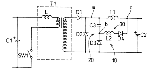
Referring to Fig. 1, a primary side smoothing
capacitor Cl smoothes a full wave rectified voltage applied
thereacross. A converter transformer T1 includes a
primary coil and a secondary coil while a~ leakage inductance
in the converter transformer T1 is especially indicated by
L. A switch element SWl is formed by a transistor and
CA 02358835 2001-10-16
connected in series to the primary coil of the converter
transformer Tl to be switched on and off for a power
transformation control.
A rectifying diode D1 is connected at an anode thereof
to an end of the secondary coil of the converter transformer
Tl. A choke coil Ll is connected in series to a cathode
of the rectifying diode D1. In other words, the choke coil
L1 is indirectly connected to the secondary coil of the
converter transformer Tl through the z~ectifying diode D1.
The choke coil L1 functions as a smoothing magnetic
substance by storing energy at a time of a turn-on of the
switch element S1 and releasing the energy at a time of a
turn-off of the switch element Sl.
A commutating diode D2 is connected to a connecting
portion of the rectifying diode Dl and the choke coil Ll.
The commutating diode D2 functions as a diode which releases
the energy stored in the choke coil L1.. A secondary side
smoothing capacitor C2 is connected in parallel to the choke
coil Ll and the secondary coil of the converter transformer
T1.
The operation of the forward scheme switching power
supply essentially structured in the above manner is
well-known and therefore detailed des~:,ription is omitted
here. In this case, the switching power supply is of a
circuit scheme carrying out power 'transformation for
obtaining a stable current or voltage and typically
includes a detecting circuit of an output voltage or a
controller circuit stably controlling an output voltage at
a constant value through the control o:~ the switch-on and
-off cycle of the switch element SW1 in accordance with the
detected voltage, however, these circuits are not shown in
the figures in the present embodiment.
11
CA 02358835 2001-10-16
A snubber circuit 10 includes a first series circuit
20 of a capacitor C3 and a diode D3 and a second series
circuit 30 of a coil L2 and a diode D4.
The first series circuit 20 is connected in parallel
to the commutating diode D2. In the first series circuit
20, the capacitor C3 is connected to a choke coil connecting
side (magnetic substance connecting side) "a" in the
commutating diode D2. In this case, the choke coil
connecting side "a" corresponds to the: cathode side of the
commutating diode D2.
The second series circuit 30 is connected between a
connecting portion "b" of the capacitor C3 and the diode
D3 in the first series circuit 20 and a commutating diode
non-connecting side "c" in the choke coil Ll.
Referring to Figs . 2A to 2D, in voltage and current
waveforms with a switch-on and -off oi° the switch element
SWl, a voltage Vswl of the switch elemenit SWl varies as shown
in Fig. 2A. A current ISWl of the switch element SW1 varies
as shown in Fig. 2B. A current IDl of t;he rectifying diode
D1 varies as shown in Fig. 2C. A current IDZ of the
commutating diode D2 varies as shown in Fig. 2D.
Referring to Fig. 3 and Figs. 10A to 10F, the a
suppression of voltage ringing at a time of a switch-off
of the switching device SWl is described in terms of mode
1 to mode 7.
In each mode, the sense of a current flow is indicated
by an arrow.
Fig. 10A shows the voltage VS~,1 (collector voltage)
applying to the switch element SW1, Fig. lOB shows the
current Iswl flowing into the switch element SW1, Fig. lOC
shows the current IDZ flowing into the: commutating diode
D2, Fig. lOD shows the current I~3 flowing into the capacitor
12
CA 02358835 2001-10-16
C3, Fig. 10E shows the voltage V~3 applying to the capacitor
C3 , and Fig. lOF shows the current ILZ f: lowing into the coil
L2.
(Mode 1)
In mode 1, as shown in Fig. 3 and Figs. 10A to 10F,
the switch element SWl is turned on at the start of mode
1. Since the switch element SW1 conducts, the voltage Vswl
thereof is approximately zero and the current Iswl thereof
is approximately constant at a predetermined value.
The current Ip2 of the commutating diode D2 is zero .
The current I~3 of the capacitor C3 increases to a
negative side during a period that the atored energy amount
of the capacitor C3 from start to halfway of mode 1 is small,
turns to decreasing in the course of increasing the stored
energy, and stops flowing when the stored energy of the
capacitor C3 is full at an end of mode 1.
The voltage V~3 of the capacitor C3 increases to
positive until the end of mode 1, and the current IL2 of
the coil L2 increases and then turns to decreasing in
halfway .
Current flows to the smoothing capacitor C2 via a
first path consisting of the secondary coil of the converter
transformer T1, the rectifying diode D.l and the choke coil
L1, and a second path consisting of that secondary coil,
the capacitor C3, the coil L2 and the; diode D4.
(Mode 2)
In mode 2, as shown in Fig. 4 and Figs. 10A to 10F,
the voltage Vswl and current Iswl of the switch element SWl
and the current IDZ of the commutating diode D2 do not change
at all. Since the capacitor C3 is already stored the energy
13
CA 02358835 2001-10-16
and in a full charged state, the current I~3 does not flow
in, whereby the voltage V~3 of the capacitor C3 is
approximately constant. While the coil L2 flows the
current IL2 as a power source by the stored thereof even
if the current is cut off from the capacitor C3, the current
IL2 gradually decreases due to the decreasing of the energy
thereof .
Current flows to the smoothing capacitor C2 via a
first path consisting of the secondary coil of the converter
transformer Tl, the rectifying diode D1 and the choke coil
L1, and a second path consisting of the diode D3, the coil
L2, and the diode D4.
(Mode 3)
As shown in Fig. 5 and Figs. 10A to 10F, when mode
3 is started, the switch element SW1 is turned off. Due
to the turn-off , the voltage VS~1 of the: switch element SWl
starts to increasing while the current: Iswl thereof starts
to decreasing.
A current continues to flow into the choke coil L1
even when starting of mode 3. Further, the commutating
diode D2 does not conduct throughout; mode 3, with the
current IDZ equal to zero .
Under the conditions, as the sw~!_tch element SWl is
turned off, the voltage of the secondary coil of the
converter transformer T1 becomes to decreasing. As a
result, the voltage stored in the capacitor C3 is more
higher, so that the current I~3 flows from the capacitor
C3 into choke coil L1. The current I~3 continues to increase
gradually until the end of mode 3.
Since the current I~3 is gradually increased, the
current Isxl of the switch element SWl is gradually and
14
CA 02358835 2001-10-16
smoothly decreased throughout mode 3. Accordingly, a
ringing of the voltage Vswl of the switch element SW1 is
suppressed in mode 3.
Current flows to the smoothing capacitor C2 via a
first path consisting of the secondary coil of the converter
transformer Tl, the rectifying diode T~1 and the choke coil
L1, a second path consisting of the diode D3, the capacitor
C3 and the choke coil L1, and a thirds path consisting of
the diode D3, the coil L2 and the diode D4.
(Mode 4)
Referring to Fig. 6 and Figs. 10A to 10F, although
the switch element SW1 is in the course of turn-off from
start to first half of mode 4, a current does not become
to flowing into the choke coil L1 through the rectifying
diode D1.
Although The current I~3 from the; capacitor C3 flows
into the choke coil L1, the current I~~, is almost constant
throughout mode 4. Accordingly, the current IDZ does not
also flow into the commutating diode D:~ throughout mode 4.
A current flows to the smoothing capacitor C2 via a
first path consisting of the diode D3 , ithe capacitor C3 and
the choke coil L1, and a second path consisting of the diode
D3, the coil L2 and the diode D4.
(Mode 5)
In mode 5, as shown in Fig. 7 and Figs. 10A to 10F,
the current from the capacitor C3 starts decreasing, so that
the commutating diode D2 conducts to sest the choke coil L1
as a current source, whereby the currenlt IDZ starts to flow.
A current flows to the smoothing capacitor C2 via a
first path consisting of the commutating diode D2 and the
CA 02358835 2001-10-16
choke coil L1, a second path consisting of the diode D3,
the capacitor C3 and the choke coil L1, and a third path
consisting of the diode D3, the coil L2 and the diode D4.
(Mode 6)
In mode 6, as shown in Fig. 8 and Figs. 10A to 10F,
the current I~5 from the capacitor C3 does not become to flow
and the current ID2 flowing into the commutating diode D2
is also approximately constant.
A current flows to the smoothing capacitor C2 via a
first path consisting of the commutat:Lng diode D2 and the
choke coil L1, and a second path consisting of the diode
D3, the coil L2 and the diode D4.
(Mode 7)
In mode 7, as shown in Fig. 9 and Figs. 10A to 10F,
the voltage VS~1 of the switch element SW1 is also stable.
A current flows to the smoothing capacitor C2 via a
path consisting of the commutating diode D2 and the choke
coil L1.
In modes 1 to7 mentioned above; in the case of the
embodiment of the invention, since the; current ISW1 of the
switch element SWl gradually decreases :in mode 3 at the time
of the turn-off of the switch element SW:1, a voltage ringing
at the time of the turn-off of the sw~_tch element SW1 is
suppressed even if the primary coil of the converter
transformer Tl has a large leakage inductance.
In addition, since the snubber circuit 10 is formed
by the capacitor C3, the diodes D3 and L~4, and the coil L2,
an energy loss in the snubber circuit 10 can approximately
be prevented.
The snubber circuit 10 is provided in the secondary
16
CA 02358835 2001-10-16
side of the switching power supply" thereby employing
components in which a rated voltage and a shape dimension
are small.
Referring to Figs. 11 to 20, when a fly-back switching
power supply in accordance with another preferred
embodiment of the invention is described, the switching
power supply is provided with a snubbe:r circuit 10. Like
the embodiment mentioned above , the snubber circuit has a
first series circuit 20 consisting of a capacitor C3 and
a diode D3, and a second series circuit 30 consisting of
a coil L2 and a diode D4.
The first series circuit 20 is connected in parallel
to the commutating diode D2.
In the first series circuit 20, the capacitor C3 is
connected to a secondary coil conneci~ing side (magnetic
substance connecting side) "a" of the converter transformer
T1 in the commutating diode D2.
The second series circuit 30 is connected between a
connecting portion "b" of the capacitor C3 and the diode
D3 in the first series circuit 20, and a commutating diode
non-connecting side "c" in the secondary coil as a magnetic
substance.
Referring to Figs . 12A to 12C, the voltage VS~,1 of the
switch element SW1, as shown in Fig. 12A, and the current
Iswl thereof, as shown in Fig. 12B, vary respectively. Than
the current IDZ of the commutating diode; D2 varies as shown
in Fig. 12C.
Figs. 13 to 19 show modes 1 to '7 respectively.
Figs_ 20A to 20F correspond to Figs. 10A to 10F
respectively.
(Mode 1)
17
CA 02358835 2001-10-16
As shown in Fig. 13 and Figs . 20A to 20F, the switch
element SWl is turned on at the start of mode 1. The voltage
VsWl of the switch element SW1 is appro~;imately zero and the
current ISWl through the switch element SW1 is approximately
constant at a predetermined value. T:he current Ip2 of the
commutating diode D2 is zero.
In the snubber circuit 10, the; current I,., of the
capacitor C3 increases to negative, then turns to
decreasing in halfway, and finally stops flowing at the end
of mode 1 in which the energy storing amount of the capacitor
C3 becomes in a full state. No current flows to the
smoothing capacitor C2 since the commutating diode D2 i.s
switched off .
(Mode 2)
In mode 2, as shown in Fig. 14 and Figs. 20A to 20F,
the current I~3 is flowing since the capacitor C3 is already
stored the energy and in a full charged state. The coil
L2 becomes a current source by the energy stored therein
and current ILZ flows therefrom. Accordingly, a current
flows to the smoothing capacitor C2 vi,a a path consisting
of the coil L2, the diode D4 and the diode D3.
(Mode 3)
In mode 3, as shown in Fig. 15 and Figs. 20A to 20F,
the switch element SW1 is turned off, the voltage VS~,1 of
the switch element SW1 starts increasing, and the current
Iswl thereof starts decreasing.
In this case, the current Iswl of the switch element
SW1 is smoothly and gradually decreased from starting to
ending of mode 3 due to the current I~,3 supplied from the
capacitor C3, so that the voltage Vsxl of' the switch element
18
CA 02358835 2001-10-16
SW1 increases such a gradient that a voltage ringing is
suppressed from starting to ending of mode 3.
Accordingly, a current flows into the smoothing
capacitor C2 via a path consisting of the secondary coil
of the converter transformer T1, the <:apacitor C3 and the
diode D3, and a path consisting of thE: coil L2, the diode
D4 and the diode D3.
(Mode 4)
Reference a.s made to Figures 16 and 20A-20F . In mode
4, current flows to the smoothing capacitor C2 via a path
formed by the secondary coil, the capacitor C3, and the
diode D3 and another path formed by the coil L2, the diode
D4, and the diode D3.
(Mode 5)
In mode 5, as shown in Fig. 17 and Figs. 20A to 20F,
the current IDZ starts flowing into the commutating diode
D2 while the current I~3 of the capacitor C3 starts
decreasing.
A current flows to the smoothing capacitor C2 via a
path consisting of the secondary coil .and the commutating
diode D2, a path consisting of the secondary coil, the
capacitor C3 and the diode D3 , and a path consisting of the
coil L2, the diode D4 and the diode D3.
(Mode 6)
In mode 6, as shown in Fig. 18 and Figs. 20A to 20F,
the current I~3 does not flow from the capacitor C3, and
a current flows to the smoothing capacitor C2 via a path
consisting of the secondary coil and the commutating diode
D2, and a path consisting of the coil L2, the diode D4 and
19
CA 02358835 2001-10-16
the diode D3.
(Mode 7)
In mode 7 , as shown in Fig . 19 a:nd Figs . 20A to 20F ,
a current flows to the smoothing capacitor C2 via a path
consisting of the commutating diode D~2 and the secondary
coil.
In the embodiment mentioned above, like the
embodiment mentioned above, the voltage ringing at the time
of the turn-off of the switch element SW1 is suppressed.
In addition, since the snubber circuit 10 a.s provided
With the capacitor C3 , the diodes D3 and D4 , and the coil
L2, the energy loss in the snubber circuit 10 can be
approximately prevented.
The snubber circuit 10 is provided in the secondary
side of the switching power supply, thereby employing
components in which a rated voltage and a shape dimension
are small.
Referring to Figs. 21 to 30, when a tapped inductor
scheme switching power supply in accordance with another
further preferred embodiment of the invention is described,
the switching power supply includes a primary side
smoothing capacitor C1, a switch element SW1, a tapped
inductor L3, a secondary side smoothing capacitor C2, a
commutating diode D2 and a snubber circuit 10.
Such operation of the switching power supply is
well-known and therefore the description is omitted.
The switching power supply is provided with the
snubber circuit 10. Like the embodiment mentioned above,
the snubber circuit 10 has a first series circuit 20
consisting of a capacitor C3 and a diode D3 and a second
series circuit 30 consisting of a coil L2 and a diode D4.
CA 02358835 2001-10-16
The first series circuit 20 is connected in parallel
to the commutating diode D2.
In the first series circuit 20, the capacitor C3 is
connected to a tapped inductor connecting side (magnetic
substance connecting side) "a" in the commutating diode D2.
In this case, the secondary coil connecting side "a"
corresponds to the cathode side of the commutating diode
D2.
The second series circuit 30 is connected between the
connecting portion "b" of the capacitor C3 and the diode
D3 in the first series circuit 20 and the commutating diode
non-connecting side "c" in the tapped inductor L3.
Referring to Figs. 22A to 22C, the voltage VSWl of the
switch element SW1, as shown a.n Fig. :?2A, the current Iswl
thereof, as shown in Fig. 22B, vary respectively. The
current IDZ of the commutating diode D:? varies as shown in
Fig. 22C.
Figs. 23 to 29 show modes 1 to 7 respectively.
Figs. 30A to 30F correspond to Figs. 10A to lOF
respectively.
(Mode 1)
In mode l, as shown in Fig. 23 arid Figs. 30A to 30F,
the switch element SWl is turned on. The voltage Vswl of
the switch element SW1 is approximately zero and the current
ISWl of the switch element SWl is approximately constant at
a predetermined value. The current IDZ of the commutating
diode D2 is zero.
The current I~3 of the capacitor C3 increases to
negative, then turns to decreasing, and stops flowing of
current into the capacitor C3 when the er.~ergy storing amount
of the capacitor C3 becomes in a full state at ending of
21
CA 02358835 2001-10-16
mode 1.
(Mode 2)
In mode 2, as shown in Fig. 24 and Figs. 30A to 30F,
the voltage Vswl and current Iswl of the: switch element SWl
and the current IDZ of the diode D2 are: absent . Since the
capacitor C3 is already stored the energy and in a full
charged state, no current I~3 flows into the capacitor C3.
(Mode 3 )
as shown in Fig. 25 and Figs. 30A to 30F, mode 3 is
entirely turn-off period of the switch element SW 1. At
the start of mode 3, the voltage VS~,l of the switch element
SWl starts increasing and the current IS~,1 thereof starts
decreasing.
In this case, the current I5~,1 of the switch element
SWl is smoothly and gradually decreased from starting to
ending of the mode 3 due to the current I~3 supplied from
the capacitor C3 , so that the voltage; Vswl of the switch
element SW1 increases such a gradient that the voltage
ringing is suppressed from starting to ending of mode 3.
(Mode 4)
In mode 4, as shown in Fig. 26 and Figs. 30A to 30F,
a current flows to the smoothing capacitor C2 via a first
path consisting of the diode D3, the; capacitor C3 and
another coil L32 of the tapped inductc>r L3, and a second
path consisting of the diode D3, the coil L2 and the diode
D4.
(Mode 5)
In mode 5, as shown in Fig. 27 and Figs. 30A to 30F,
22
CA 02358835 2001-10-16
the current IDZ starts flowing into the commutating diode
D2 while the current I~3 of the capacitor C3 starts
decreasing.
A current flows to the smoothing capacitor C2 via a
first path consisting of the commut;ating diode D2 and
another coil L32 of the tapped inductor L3, a second path
consisting of the diode D3, the capacsitor C3 and another
coil of the tapped inductor L3, and a tlhird path consisting
of the diode D3, the coil L2 and the diode D4.
(Mode 6)
In mode 6, as shown in Fig. 28 and Figs. 30A to 30F,
the current I~3 does not flow from the capacitor C3.
A current flows to the smoothing capacitor C2 via a
first path consisting of the commutating diode: D2 and
another coil L32 of the tapped inductor L3, and a second
path consisting of the diode D3, the coil L2 and the diode
D4.
(Mode 7)
In mode 7, as shown in Fig. 29 arid Figs. 30A to 30F,
a current flows to the smoothing capacitor C2 via a path
consisting of the commutating diode D2 and another coil L32
of the tapped inductor L3.
The present embodiments can be. also obtained an
operating effect same: as mentioned above.
Further, Examples of the forward scheme switching
power supply of the invention include those shown in Figs .
31 to 33. The invention is applicable; likewise to these
switching power supplies. The primary side of the
converter transformer T1 is not shown in Figs. 31 to 33.
Further, in the case of Figs . 32 and 33 , the choke coil L1
23
CA 02358835 2001-10-16
is directly connected to the secondary coil of the converter
transformer T1.
Examples of the fly-back scheme switching power
supply of the invention include those shown in Figs . 34 to
36. The invention is applicable likewise to these
switching power supplies. the primary side of the
converter transformer T1 is not shown in Fig. 34 to 36.
Examples of a tapped inductor scheme switching power
supply of the invention include those shown in Figs . 37 to
39. The invention is applicable likewise to these
switching power supplies. the switch, element SWl is not
shown in Figs. 37 to 39.
the invention is applied as a power transformer to
a switching power supply. Nevertheless, this is by no means
meant to be limiting the scope and spirit of the invention.
The invention is also applicable to other power
transformers, such as an inverter.
While there has been described what is at present
considered to be preferred embodiments. of this invention,
it will be understood that various modifications may be made
therein, and it is intended to cover in the appended claims
all such modifications as fall within the true spirit and
scope of this invention.
24