Note: Descriptions are shown in the official language in which they were submitted.
CA 02358897 2001-06-29
WO 00/39860 . PCT/RU99/00245
INJECTION INCOHERENT EMITTER
Field of the Invention
The invention relates to optoelectronics technology, and specifically to
efficient,
high-power, superluminescent and compact semiconductor diode spontaneous
emission
sources with a narrow radiation pattern.
Prior Art
An injection incoherent emitter (hereinafter referred to as "Emitter") is a
device that converts electrical energy to optical radiation energy of a
specified
spectral composition and spatial distribution (in the absence of an optical
resonator).
Various types of injection incoherent emitters are known for a broad range of
wavelengths, from infrared to blue and ultraviolet radiation: surface-emitting
light-
emitting diodes, including luminescent multipass light-emitting diodes [F.A.
Kish et al.,
Appl. Phys. Lett., v.64, No. 20, pp. 2839-2841 (1994); H. Sugawara et al.,
Jap. J. Appl.
Phys., v.31, No.8, pp. 2446-2451 (1992); 3 M. Watanabe, et al., US Patent, No.
5,537,433, July 16, 1996; S. Nakamura et al., Jap. J. Appl. Phys. Lett., v.34,
L1332,
(I995)] and edge emitters [A.T. Semenov et al., Electron. Lett., v.29, pp. 854-
857,
(1993); G.A. Alphonse et al., IEEE J. of Quant. Electronics, v.QE-24, pp.2454-
2457,
(1988)]. Further broad application of these radiation sources has been impeded
by
insufficiently high efficiency, radiation intensity and _power and also, for a
number .of
applications, by the large divergence of the radiation.
The known Emitter from [F.A. Kish et al., Appl. Phys. Lett., v.64, No.20, pp.
2839-2841 (1994)] is multipass and includes a heterostructure based on the
semiconductor compounds AIGaInP, containing an active layer with bandgap Ea
(eV),
thickness da within the range 1 ~m to 1.5 ~m and two cladding layers (p-type
and n-type
conductivity) of optically homogeneous layers consisting of a single sublayer
and
disposed respectively on the first and opposite second surfaces of the active
layer. The
inner surfaces of area S;~ pm2 of two radiation output regions are placed, one
on each
side, on the surfaces of the cladding layers that are remote from the active
layer; said
radiation output regions (hereinafter referred to as ROR) are made from the
homogeneous
semiconductor compound GaP, that is transparent to the radiation
Page 3
CA 02358897 2001-06-29
WO 00/39860 PCT/RU99/00245
2
and of p-type and n-type conductivity, in the shape of rectangular
parallelepipeds. 'The
lateral surfaces of the parallelepipeds make linear angles of inclination yr
of 90° with the
inner and outer surfaces, and also with the plane of the active layer. The
charge carrier
injection region, of area SIR (wm2), coincides with the active layer and is
formed by
ohmic contacts made respectively to the p-type and n-type radiation output
regions. The
required corresponding metallization layers are present. When a d.c. current
is applied,
recombination of nonequilibrium carriers occurs in the injection region with
generation of
spontaneous emission, propagating in all directions from the injection region,
including
toward both p-type and n-type output regions. After random multiple
reflections, a certain
fraction of the spontaneous emission exits at various angles from the light-
emitting diode
through the output surfaces. The latter are partially located on the outer
surface of the p-
type output region and the lateral surfaces of the output regions of both
types. The angle
of divergence 91 of the output radiation in the vertical planes and the angle
of divergence
82 of the output radiation in the horizontal planes have the maximum
permissible values
(up to 180°) in this case. Here and in the following, we define the
vertical planes as the
planes perpendicular to the plane of the active layer. We define the
horizontal planes as
the planes that are perpendicular to the vertical planes and located on the
output surfaces.
Note that to each direction of the radiation passing through the horizontal
plane may
correspond its own vertical plane, containing radiation beams of the
aforementioned
direction. For a wavelength of 604 nm, the known Emitter [F.A. Kish et al.,
Appl. Phys.
Lett., v.64, No.20, pp.2839-2841, (1994)] has external efficiency 11.5% and
optical
power of the radiation (for a current of 1 A) 93.2 lm/A. Its operating current
density for
continuous wave (cw) operation is no higher than 100 A/cm2. In this case, the
direction of
the light beams relative to the output surfaces is chaotic (random).
Disclosure of the invention
The problem addressed by the invention is to design an Emitter with increased
external efficiency, power, optical power, radiation intensity, and optical
radiation
intensity, with the ability to realize directional spontaneous emission with a
broad
range of directions for its output, including design of multibeam Emitters,
linear and
Page 4
CA 02358897 2001-06-29
PCT/RU 99/00245
JUNE 1, 2000 (06/01/2000)
3/1
two-dimensional emitter arrays, including those with beams that may be
independently switched on, while simplifying the technology for making them.
According to the invention, the problem addressed is solved by proposing an
injection incoherent emitter, comprising a heterostructure containing an
active layer,
cladding layers, ohmic contacts, and at least on one side of the active layer,
adjacent to
the heterostructure, a radiation output region that is transparent to the
radiation; and at
least one radiation output region is made and said output region has at least
one layer
characterized by refractive index nRORq, optical loss factor for the radiation
aRORq
(cm-I), thickness dRORq (N~m), where q = l, 2, . . . , p are defined as
integers that
designate the sequential numbers labeling the layers of the output region, as
counted
from its boundary with the heterostructure; and the heterostructure with the
adjoining
radiation output region is characterized by an effective refractive index
neff, where the
effective refractive index ne ff and the refractive index nRORI ~'e selected
to satisfy the
relations:
0 < (arccos(neff/nROR1)) - ~P ~ ~'~COS ( neff min/nROR1) - ~Pmax~ ~d neff min
is
greater than nr,.,;~, where neff min is the minimum value of neff of all
possible neff for the
multitude of heterostructures with radiation output regions that are of
practical value,
nmin is the smallest of the refractive indices in the cladding layers of the
heterostructure,
cp is the angle of propagation, made with the plane of the active layer by the
normal to the front for radiation propagating within the radiation output
region, and
~Pmax is the upper bound for possible propagation angles.
A distinction of the proposed Emitters is the essential features of the entire
heterostructure and the radiation output region, which affect the details of
their operation
and the output characteristics achieved for the Emitters. The number of layers
and
sublayers of the heterostructure, their thicknesses and composition are
selected for the
proposed Emitter to achieve a narrow radiation pattern, especially in the
vertical planes,
for intense spontaneous emission appearing in the injection region and
predominantly
directed at propagation angles cp relative to the plane of the active layer.
The necessary
condition for this is that the relation known as the leakage condition for
laser modes
propagated in
IPEA/RU
AMENDED SHEET
CA 02358897 2001-06-29
PCT/RU 99/00245
JUNE l, 2000 (06/01/2000)
3/2
the optical resonator of laser diodes [J.K. Buttler, Y. Kressel and I. Ladany,
IEEE Journ.
Quant. Electron., v.QE-11, p.402, (1975)] be satisfied:
neff ~ nRORI (1)
The effective refractive index neff can be obtained
IPEA/RU
AMENDED SHEET
CA 02358897 2001-06-29
PCT/RU 99/00245
JL11VE 1, 2000 (06/01/2000)
4
by computation from the relation (3 = (2~/~,)ne ff, where (3 is the absolute
value of the
complex wave propagation constant for the radiation in one of the directions
in the active
layer, and ~, is the radiation wavelength. In the present invention, we have
proposed and
experimentally confirmed that condition (1) is also applicable to spontaneous
emission.
Accordingly, the propagation angle cp for directional spontaneous emission is
defined as
equal to the leakage angle for the laser modes, and specifically
cp = arccos (neff/nROR1) (2)
We further propose using the entire range of propagation angles cp for
directional
spontaneous emission, and accordingly the entire range of the ratios
(neff/nROR1).
Relations (1) and (2) determine the lower bound for the angle cp (cp greater
than zero). We
propose to determine the upper bound for the propagation angles in question,
cpnax, using
the relations:
arccos(neff/nRORI) "~ arccos (neff min/nRORl) _ ~pmax (3)
neff min is greater than nn,;r, (4)
where neff min is the minimum value of neff of all possible neff for the
multitude of
heterostructures 2 with radiation output regions 7 that are of practical
value, and n~ is
the smallest of the refractive indices in the cladding layers of the
heterostructure.
Numerical calculations we carried out for some heterostructures that are of
practical use,
such as ones based on compounds InGaAs/GaAs/AIGaAs, showed that the maximum
leakage angle cpmax is approximately equal to 30° to 35°.
The angle of divergence ~cp in the vertical planes for spontaneous emission
propagating in the output region is determined by the spectral dispersion
(i.e., by the
spread in the propagation angle cp as a function of the wavelength ~,, that
varies within the
spectral band ~~, for spontaneous emission) and by diffraction. The angle of
dispersion-
limited divergence ~cpl may be determined by a numerical calculation using
formula (2)
for known dependences of the refractive indices neff and nRORI on the
wavelength ~,
(within the range ~~,). The angle of diffraction-limited divergence Ocp2, when
using a
known approximate relationship [H. C. Casey and M. B. Panish, Heterostructure
Lasers,
Pt. 1 [Russian translation], Izdat. Mir, Moscow (1981), pp. 89-97], may be
written as
Ocp2 ~ Y . ~,/(neffDIR~sin cp),
where y is a numerical coefficient indicating at what radiation intensity
level the angle
Ocp is determined ('y is equal to unity for level 0.5, and 'y is equal to two
IPEA/RU
AMENDED SHEET
CA 02358897 2001-06-29
PCT/RU 99100245
JUNE l, 2000 (06/01/2000)
for level 0.1), and DIR is the size of the injection region in the plane of
the active layer in
the selected direction. The total angle of divergence Ocp for radiation in the
vertical plane
inside output region 7 is equal to (4cpl + Ocp2). The angle of divergence O1
for the output
radiation in the vertical plane outside the output region is determined using
the familiar
Fresnel formulas [R. W. Ditchburn, Physical Optics [Russian translation of
Ditchburn's
Light], Izdat. Nauka, Moscow (1965), pp. 398-402], and specifically O1 is
approximately
equal to arcsin [n~sin(~cp)]. Considering that the angle Ocp is small, the
angle O1 can be
estimated as
~1 ~ (nROR1/n0)Wcp (6)
where np is the refractive index of the medium bounding the output surface
(for air, np is
equal to unity).
For the directional spontaneous emission obtained, its input efficiency r);"
in the
output region is determined by the ratio of the number of spontaneous photons,
traveling
at propagation angles from (c~ - Ocp/2) to (cp + O~p/2) from the injection
region to the
output region, to the total number of spontaneous photons in the injection
region. We
found that rlin can be defined as
Olin - aOR/(aOR + aIR + aend)~
where g (cm-I) is the gain for the radiation in the heterostructure due to the
injection
current density j (A/cm2), aIR (cm-I) is the optical loss factor determined by
absorption
and scattering of radiation within the injection region, aend (cm-I) is the
loss factor
determined by radiation leaking through the end boundaries of the injection
region, and
apR is the net loss factor for outgoing directional spontaneous emission
leaking from the
injection region to the output region. Consequently, the input efficiency
rl;", determining
to a significant extent the external efficiency of the Emitter, is mainly
controlled by the
thickness and/or the composition (refractive index) of the cladding sublayers
adjacent to
the output region. If we choose apR » (aIR + aend)~ then we may obtain rl;I,
close to
unity. Depending on the characteristics of the cladding layers, either one-
sided or two-
sided output of spontaneous emission from the injection region can be
realized.
The underlying assumption of the present invention, that an appropriate choice
for
the heterostructure can result in generation of narrowly directed spontaneous
emission, is
not obvious. It is widely believed that spontaneous emission within a
heterostructure is
nondirectional because of the random nature of propagation of individual
spontaneous
photons (see, for example, [Yu. R. Nosov, Optoelectronics, Moscow, Izdat.
IPEA/RU
AMENDED SHEET
CA 02358897 2001-06-29
WO 00/39860 PCT/RU99/00245
6
Radio i Svyaz (1989), p.141]). We have experimentally demonstrated and
confirmed by
computation that upon implementation of our proposed aggregate of essential
features for
the proposed Emitter, we achieve a narrow radiation pattern for the
spontaneous emission
in the vertical planes with subsequent efficient output of the emission, which
leads to
ultrahigh external efficiency, power, optical power, radiation intensity, and
optical
radiation intensity; the ability to output radiation in different controllable
directions,
including in the direction perpendicular to the active layer; realization of
multibeam
Emitters, including linear and two-dimensional emitter arrays with
independently
controllable beams.
All the noted essential features of the invention made it possible to realize
the
proposed Emitter in various modifications, considered below, and specifically
modifications having different compositions, widths, thicknesses, and numbers
of
layers, sublayers, and regions belonging both to the heterostructure and to
the output
region, and also to realize various different as well as unusual
configurations of the
output region in order to obtain high-efficiency output of directional
spontaneous
emission.
In selecting the design of the output region, we started from the fact that
with the
distinctive features we have introduced, the spontaneous emission has a narrow
radiation
pattern in the vertical planes, but in the corresponding horizontal planes,
its propagation
is equally likely (within a range of 2~) in any direction (in contrast to the
leaky mode in
injection lasers). (Here, as in the known emitter [F. A. Kish et al., Appl.
Phys. Lett., v.64,
No.20, pp.2839-2841, (1994)), the horizontal plane is defined as the plane
perpendicular
to the corresponding vertical plane, which in turn is perpendicular to the
plane of the
active layer). This determined the dependence of the output efficiency of
spontaneous
emission from the output region on its configuration and in turn on the angles
of
inclination yr made by the generatrices of the lateral surface of the
radiation output region
with its inner surface. The highest efficiency can be achieved if we select
the output
region in the form of a solid of revolution relative to the axis perpendicular
to the plane of
the injection region and passing through its center, for example, as a
truncated right cone
or a right circular cylinder. Different directions of the radiation output
(relative to the
plane of the active layer) are realized by appropriately choosing the angles
of inclination
fir, depending on the angle cp. In individual cases, the output region may be
implemented
not only as a solid of revolution, but also, for example, as a hexahedron, but
in this case
the radiation output efficiency from the output region will be reduced.
Page 8
CA 02358897 2001-06-29
WO 00/39860 PCT/RU99/00245
7
The problem addressed is also solved in the following cases.
The active layer may be formed of at least one sublayer. The cladding layers,
disposed
respectively on the first and opposite second surfaces of the active layer,
are formed of
the cladding sublayers Ii and IIj respectively, where i = I, 2 ... k and j =
1, 2, ... m are
defined as integers that designate the sequential numbers labeling the
cladding
sublayers, as counted from the active layer, with refractive indices nI; and
nilj,
respectively, and at least one cladding sublayer is made in each cladding
layer.
In this case, heterostructure designs are possible in which at least one
cladding
sublayer may be implemented as a gradient layer, that is, with a monotonically
varying
composition. Such a gradient cladding layer is considered as a finite number
of sublayers
of a cladding layer with corresponding nip and nIIj, obtained by subdividing
each gradient
layer. The proposed heterostructure designs, for which the active layer may be
made as
one or several active sublayers (including sublayers having quantum-sized
thicknesses),
isolated from each other by barrier sublayers, and the cladding layer may be
made as a
gradient layer, or consisting of one or several sublayers, make it possible to
increase the
internal efficiency of conversion of injected nonequilibrium carriers to
spontaneous
photons and to thus increase the efficiency of the Emitter as a whole.
The solution to the addressed problem is also achieved as follows.
At least one injection region is made in the working amplifier. The injection
region in
the working device in practice coincides with the active layer for the portion
of it (the
area) in which injection of nonequilibrium carriers occurs. The presence of a
series of
injection regions makes it possible to create multibeam Emitters.
In the preferred embodiments, the thickness of the cladding layer adjacent to
the
radiation output region is selected to be less than the thickness of the
cladding layer
disposed on the opposite side of the active layer and/or the refractive index
of the
cladding sublayer adjacent to the radiation output region is selected to be
greater than the
refractive index of the outer cladding sublayer, disposed on the opposite side
of the active
layer.
The proposed development of the features of the invention results in
unidirectional
propagation of spontaneous emission from the injection region to the radiation
output
region, with substantial improvement of the directionality and an increase in
the external
efficiency.
Page 9
CA 02358897 2001-06-29
PCT/RU 99/00245
J(JNE 1, 2000 (06/01/2000)
8
Of course, the direct projection of the injection region onto the inner
surface of
the output region should not go beyond its limits. The choice of the thickness
dRORI
depends on the propagation angle cp, the maximum dimension of the injection
region DIR,
and the angles of inclination yr. Accordingly, in the preferred embodiments of
the
Emitter, in order to solve the problem addressed, it is expedient: to select
the dimensions
and area SIR of the injection region to be no greater than the dimensions and
area S;" of
the introduced inner surface of the radiation output region, adjacent to the
heterostructure,
and to select the thickness of the radiation output region dRORq from the
range 1 to
10,000 pm.
In a number of cases: the radiation output region should be implemented as
electrically conductive, and ohmic contact should be made to the introduced
outer surface
of the radiation output region. This makes it possible to simplify the
fabrication
technology for the Emitter.
In preferred embodiments of the Emitter, in order to solve the problem
addressed,
the radiation output region is made of optically homogeneous material. The
requirement
that the output region be transparent to the spontaneous emission means that
for efficient
operation of the Emitter, we need to have small optical losses due to
absorption and
scattering of spontaneous emission in the output region. For an output region
consisting
of a single layer, this will be the case if the following condition is
satisfied:
aROR1 « (N-'Din) I
where p is a number which, depending on the configuration of the output
region, may
vary approximately from 0.4 to 1.5; and D;n is the dimension of the inner
surface of
output region in the selected direction. For example, for semiconductive
materials, the
bandgap ERORI for the output region should be greater than the bandgap Ea of
the active
layer, which is determined by the wavelength ~.. In cases when in order to
achieve low
values of aROR1 (cm-I) the output region becomes nonconducting, it is
expedient to
make the radiation output region from at least two layers, where the first
layer, bordering
the heterostructure, is made electrically conductive and the second layer is
made from a
material having a lower optical loss factor aRpR2 than aROR1 for the first
layer, and in
this case the second layer may be made insulating. The above makes it possible
to
increase the efficiency of the Emitter as a result of the reduction in the
optical losses due
to absorption and scattering of radiation as it passes through the output
region.
We can control propagation of radiation in layers of the output region, and
consequently the thickness of the output region and its layers, by selecting
different
refractive indices nRORI for the first layer and nRpRZ for the second layer.
In this case, in
the first layer, radiation
IPEA/RU
AMENDED SHEET
CA 02358897 2001-06-29
PCT/RU 99/00245
JI1NE 1, 2000 (06/01/2000)
9/1
propagates at a propagation angle cp equal to arccos ( neff/nROR1) (see (2)),
and in the
second layer it propagates at a propagation angle cp2 equal to arccos
(neff/nROR2) (see
(2)). Analogously, for the q-th layer of the output region, the following
relation is
satisfied:
cpq = arccos ( neff/nRORq) (9)
Thus the angle of propagation cpq at the boundary between two layers of the
output region will change on either side. For example, for an output region
consisting of
two layers, if the refractive index nRp~ of the second layer is selected to be
greater than
the refractive index nROR1 of the first layer, bordering the heterostructure,
then the angle
cp2 will be greater than the angle cp. For the opposite case: when nRp~ is
less than
nRORI~ then the thickness of the second layer can be made smaller than in the
preceding
case, which leads to a decrease in the thickness of the output region, and
also to
simplification of the fabrication technology and reduction in the fabrication
costs for the
Emitter. Further simplification of the technology and decrease in the
thickness dRORI of
the output region, all the way down to micron dimensions, is possible if nRp~
is selected
as less than neff. In this case, the radiation leakage condition (I) is not
satisfied for the
second layer of the output region, and at least some of the outgoing leakage
radiation at
the boundary with the second layer of the output region undergoes total
internal reflection
back into the heterostructure. Another proposed approach to decreasing the
angle of
propagation cpq involves introducing sublayers I; and/or IIj with refractive
index greater
than neff into the cladding layers of the heterostructure, having in aggregate
with the
adjoining output region an effective refractive index neff.
Further, to accomplish our objective, we propose: that at least one layer of
the
radiation output region be made from semiconductor and that at least one layer
of the
radiation output region be made from introduced substrate. This results in
simplification
of the fabrication technology for the Emitters.
In all the cases considered above of a multilayer output region with
electrically
conductive first layer, ohmic contact is made to the first electrically
conductive layer of
the output region, which results in reduction of thermal losses due to
resistance and
simplification of the fabrication technology for the Emitters. In this case,
the thickness of
the electrically conductive layer is expediently made as no greater than the
minimum
linear dimension of the injection region. The efficiency of using the proposed
embodiments of the ohmic contact depends on the dimensions of the injection
region and
on the current densities passing through the proposed Emitter. We also note
that, in the
general case, the output region may be made of not only semiconductive
materials. It is
only important that its characteristics, in particular the refractive index
nROR1 (in the
general case, nRORq (see (9)) and the optical loss factor aRORq, meet
IPEA/RU
AMENDED SHEET
CA 02358897 2001-06-29
PCT/RU 99/00245
JUNE 1, 2000 (06/01/2000)
9/2
the necessary requirements ( 1 ) and (8).
The problem addressed is also solved using various proposed modifications of
the
output region designs. A design is proposed in which the radiation output
region is
implemented as at least one truncated right circular cone, one of whose bases
is disposed
on the heterostructure. The lateral surface of the cone is formed by its
IPEAIRU
AMENDED SHEET
CA 02358897 2001-06-29
PCT/RU 99/00245
JUNE 1, 2000 (06/01/2000)
generatrices. In an Emitter with such an output region, we can realize
different directions
for the output radiation and obtain maximum efficiencies, radiation power and
intensity
for normal incidence of the radiation on the output surfaces. In this case, it
is also
proposed:
- in order to obtain a direction of radiation output at propagation angle cp
relative
to the plane of the active layer, that the linear angles of inclination y made
by the
generatrices of the lateral surface of the radiation output region with its
inner surface be
selected from the range from (~/2 - cp - a) to (~/2 - cp + 6), and 6 is the
angle of total
internal reflection on the output surface for radiation propagating within the
radiation
output region,
- in order to obtain a direction of radiation output at a right angle relative
to the
plane of the active layer on the side where the radiation output region is
disposed, that the
linear angles of inclination yr made by the generatrices of the lateral
surface of the
radiation output region with its inner surface be selected from the range from
(3~c/4 - cp/2 -
a/2) to (3~/4 - cp/2 + a/2),
- in order to obtain a direction of radiation output at a right angle relative
to the
plane of the active layer on the side where the heterostructure is disposed,
that the linear
angles of inclination y made by the generatrices of the lateral surface of the
radiation
output region with its inner surface be selected from the range from (~/4 -
cp/2 - a/2) to
(~/4 - cp/2 + 6/2).
The problem addressed is also expediently solved by implementing the output
region as at least one right circular cylinder, one of whose bases is disposed
on the
heterostructure, which permits simplification of the fabrication technology
and
achievement of high values of the characteristics for the Emitter when using
directional
multiple reflections in the output region.
An emitter is also proposed in which the output region is formed as at least
one
hexahedron, one of whose bases is disposed on the heterostructure; in this
case it is
expedient:
- that the linear angle of inclination y~, made on at least one of the lateral
surfaces
of the hexahedron with the inner surface of the output region, be selected
from the range
from (~/2 - cp - ~cp/2) to (~/2 - cp + Ocp/2), where Ocp is the angle of
divergence for the
radiation in the vertical plane,
- that the linear angle of inclination tV, made on at least one of
IPEA/RU
AMENDED SHEET
CA 02358897 2001-06-29
WO 00/39$60 PCT/RU99/00245
11
the lateral surfaces of the hexahedron with the inner surface of the output
region, be
selected from the range from (3~/4 - cp/2 - ~cp/2) to (3n/4 - cp/2 + Ocp/2),
- that the linear angle of inclination y, made on at least one of the lateral
surfaces
of the hexahedron with the inner surface of the output region, be selected
from the range
from (~/4 - cp/2 - ~cp/2) to (~/4 - cp/2 + Ocp/2),
that the linear angle of inclination yr, made on at least one of the lateral
surfaces
of the hexahedron with the inner surface of the output region, be selected as
equal to ~/2.
Choosing the design of the output region as a hexahedron makes it possible to
simplify
the fabrication technology and also to reduce the area of the near-field
radiation while
simultaneously increasing the brightness of the Emitter.
Note that for all Emitters in which the output region is made as a right
circular
cylinder or as a hexahedron, the output surface of which is perpendicular to
the plane of
the active layer, the propagation angle cp should be selected as less than the
angle of total
reflection a, which makes it possible to eliminate total internal reflection
of radiation
exiting from the radiation output region on the output surface and the
corresponding
losses.
Further, it is proposed: that antireflective coatings be applied on at least
part of the
introduced output surfaces, and also that reflective coatings be applied on
part of the
output surfaces. which makes possible an additional increase in the
efficiency, power,
intensity, and brightness of the Emitter.
Modifications of the Emitter are also proposed with a plurality of output
beams of
directional radiation. These modifications are distinguished from the
preceding
modifications in that during their fabrication, in the heterostructure at
least two injection
regions are formed with identical propagation angles cp, and when current is
independently supplied for independent control of the beams, an independent
ohmic
contact to each injection region is made on the outer side of the
heterostructure.
For one modification of the multibeam Emitter, for each injection region with
an
independent ohmic contact, an associated radiation output region may be
formed.
For another modification of the multibeam Emitter, one common radiation output
region may be formed at least for some of the injection regions, both with and
without
independent contact.
The problem addressed is also solved as follows, in order to fabricate
Emitters
with a linear sequence of output beams of directional spontaneous emission,
including
those with independent connections to the current supply:
Page 13
CA 02358897 2001-06-29
WO 00/39860 PCT/RU99/00245
12
- injection regions of identical dimensions with independent contacts are
regularly
spaced in the heterostructure along a single line, as a linear sequence of
injection regions;
- on the radiation output region side, at least on part of their outer
surfaces,
metallization layers are introduced that are implemented in the form of strips
that
electrically connect the injection regions included in the linear sequence.
To fabricate emitters with a two-dimensional array of output beams of
directional
spontaneous emission, including those with independent connections to the
current
supply, the problem addressed is solved by:
- forming at least two linear sequences of injection regions in the
heterostructure;
- on the side where the injection regions are disposed, implementing the
metallization layers on their independent contacts as strips, each of which
electrically
connects one injection region from each linear sequence of injection regions.
To increase the efficiency by reducing losses of nonequilibrium carriers due
to
their spreading and surface recombination, the injection region is expediently
limited in
size by means of introduced barrier layers, at least all the way to the active
layer
inclusive.
For more effective matching of the emitters to the power source by series
galvanic
connection of the injection regions, it is proposed that at least two adjacent
injection
regions be galvanically isolated all the way to the insulating second layer of
the output
region, and that the ohmic contacts of the aforementioned injection regions be
galvanically connected by the metallization layer.
The essence of the present invention is an original design for a
heterostructure
formed with appropriately selected compositions, thicknesses, number of layers
and
sublayers, and also a nonobvious implementation of the radiation output
region, made
from materials with specified refractive indices and number of layers, which
made it
possible to generate directional spontaneous emission with subsequent
efficient output of
the radiation from the output region. The output efficiency is additionally
increased by
selection of appropriate angles of inclination y~ of the generatrices of the
lateral surface of
the output region. All the above made it possible to increase external
efficiency, power,
optical power, radiation intensity, and
Page 14
CA 02358897 2001-06-29
WO 00/39860 PCT/RU99/00245
13
optical radiation intensity of the injection incoherent emitter, and also to
achieve
highly directional spontaneous emission in different radiation output
directions,
including design of a multibeam emitter, linear and two-dimensional emitter
arrays,
including those with beams that can each be independently switched on, with
simplification of the technology for making them.
Note that the technical realization of the invention is based on known basic
production processes, which by now are well developed. The range of radiation
wavelengths for emitters currently in use extends from infrared to ultraviolet
radiation.
The appropriate heterostructures are used for different portions of the
wavelength range.
For ultraviolet, blue, and green emission (0.36 pm < ~, < 0.58 pm), the most
effective
heterostructures are those based on semiconductor compounds in the system
AIGaN/GaN/GaInN and also ZnCdSSe/GaAs; for red and yellow (0.58 wm < ~, < 0.69
pm), compounds in the system AIGaInP/GaAs; for infrared (0.77 pm < ~, < 1.2
pm),
compounds in the system AIGaAs/GaAs and in the system InGaAs/GaAs/AIGaAs; for
infrared ( 1.2 pm < 7~ < 2.0 pm), compounds in the system GaInAsP/InP; for
infrared (2.0
pm < ~, < 4.0 um), compounds in the system AIGaInSbAs/GaAs. In each of the
indicated
ranges, depending on the ~, used and the selected heterostructure, appropriate
materials
for the output region must be selected that satisfy conditions (1) and (8). We
may suggest
the following semiconductor materials for the output region: for the system
AIGaN/GaN/GaInN - GaN; for the system ZnCdSSe/GaAs - ZnSe; for the system
AIGaInP/GaAs - GaP; for the system AIGaAs/GaAs - GaP; for the system
InGaAs/GaAs/AIGaAs - GaAs and GaP; for the system GaInAsP/InP - Si and GaAs;
for the system AIGaInSbAs/GaAs - Si and GaAs. The recently developed "wafer
bonding" technology (see, for example, H. Wada et al., IEEE Photon. Technol.
Lett. v.8,
p.173, (1996)) can be used to successfully implement these suggestions. The
designs of
efficient Emitters with directional spontaneous emission proposed by the
present
invention are applicable at least for all the above-indicated radiation
wavelength ranges
and heterostructure systems. White light emitters used for illumination may be
obtained
as follows: either by mixing radiation of the three basic colors (red, green,
and blue), or
by excitation of red and green luminescent radiation from a blue light Emitter
in a
material especially selected for this purpose.
Page 15
CA 02358897 2001-06-29
WO 00/39860 PCT/RU99/00245
14
Brief Description of the Drawings
The present invention will be understood from Figures 1-18.
Figures 1-3 schematically depict axial sections of the emitter, passing
through the
central symmetry axis of the radiation output region, made in the form of a
truncated right
circular cone, where the generatrices of the lateral surface of the radiation
output region
make the following linear angles of inclination y with its inner surface:
Fig. 1 - (~/2 - cp);
Fig. 2 - (3~/4 - cp/2);
Fig. 3 - (~/4 - cp/2).
Figure 4 schematically depicts an axial section, passing through the central
symmetry axis of the radiation output region, made in the form of a right
circular
cylinder.
Figures 5-6 schematically depict axial sections along one of the lateral sides
of the
emitters, whose output region is in the form of a rectangular parallelepiped,
and
specifically:
Fig. S: it is made from two electrically conductive layers, where the
refractive
index nRO~ of the second layer is greater than the refractive index nROR1 of
the first
layer, bordering the heterostructure;
Fig. 6: it is made from two layers, the first layer is electrically
conductive, the
second layer is insulating, and the injection layers in this case are
galvanically connected
in series.
Figures 7, 8, 9, and 10 schematically depict top views (as viewed from the
output
region) for Emitters whose axial sections are depicted in Figs. 1, 2, 4 and 5
respectively.
Figure 11 schematically depicts a transverse cross section of the proposed
emitters, mounted on a holder.
Figures 12 and 13 schematically depict respectively a longitudinal section and
a
transverse cross section of the Emitter with small nearfield radiation area
and high
brightness of the radiation, for which the radiation output is effected
through one lateral
facet of the hexahedral radiation output region.
Figures 14, 15, and 16 schematically depict respectively the sections along
and
perpendicular to the length of the linear sequence of injection regions, and
also a top view
for the Emitter with a plurality of spontaneous emission beams, for which a
common
output region is made for each linear
Page 16
CA 02358897 2001-06-29
PCTlRU 99/00245
July 27, 2000 (7/27/2000)
15/1
sequence of injection regions, in the form of a plurality of regularly spaced
and
interconnected right circular cylinders.
Figs. 17 and 18 schematically depict respectively a section along the symmetry
plane and a top view for an Emitter whose output region is made as a plurality
(nine) of
regularly spaced and interconnected truncated right circular cones.
Figure 19 presents the results of experimental measurements of the angles of
divergence of the radiation in the vertical (CJ1) and the horizontal (02)
planes.
Figure 20 presents the radiation power vs. the current passing through an
experimental model of the Emitter.
Figure 21 schematically presents a longitudinal section of an Emitter with a
one-
layer output region and different thicknesses of the cladding layer for the
middle and edge
injection regions.
Figure 22 schematically presents a longitudinal section of an Emitter with a
two-
layer output region and different thicknesses of the cladding layer for the
middle and edge
injection regions.
Figure 23 schematically represents a longitudinal section of an Emitter with
two-
layer output regions, disposed on both sides of the active layer, and
identical thicknesses
of the cladding layer for the middle and edge injection regions.
Figure 24 schematically presents a longitudinal section of an Emitter with a
one-
layer output region and identical thicknesses of the cladding layers for the
middle and
edge injection regions.
Figure 25 schematically presents a view from below for the Emitters whose
longitudinal sections are depicted in Figures 21-24.
Embodiments of the Invention
In the following, the invention is explained by specific embodiments, with
references to the attached drawings. The examples presented for the design of
the Emitter
are not the only embodiments, and suggest other embodiments whose particular
details
are reflected within the aggregate of features in the claims.
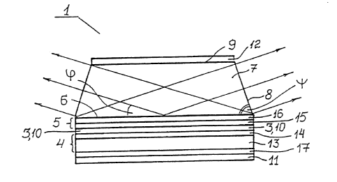
The proposed Emitter 1, one of whose modifications is schematically depicted
in
Fig. 1 and Fig. 7, includes heterostructure 2, grown by the known MOC-hybrid
epitaxy
(MOCVD) method and consisting of active layer 3,
IPEA/RU
AMENDED SHEET
CA 02358897 2001-06-29
PCT/R,U 99/00245
July 27, 2000 (7/27/2000)
15/2
disposed between cladding layers 4 and 5, with sublayers Ii and IIj
respectively, where
i = 1... k and j = 1... m. Active layer 3 in this case consists of several
active sublayers and
barrier sublayers separating them (not shown in Fig. 1 ). The inner surface 6
of
semiconductor output region 7, having the shape of a truncated right circular
cone with
lateral surface 8, the angles of inclination ~r of the generatrices of which
are equal to 72°,
is disposed on the surface of sublayer III,, of cladding layer 5 that is
remote from active
layer 3. The height of the cone is equal to 921 Vim. 'The bottom circular base
of the cone,
of diameter 3000 Vim, is the inner surface 6 of output region 7. The top base
of the cone
for output region 7 (the circle of smaller diameter, equal to 2401 Vim) is the
outer
surface 9 of output region 7. Injection region 10 in this Emitter coincides
with active
layer 3 (their areas are equal) and has a circular shape; its diameter DIR is
equal to
' 3000 Vim, its area SIR is equal to 0.07065 cm2, and its thickness is equal
to the thickness
of active layer 3. Ohmic contact 11 is made to the construction on the side
opposite the
location of output region 7, and ohmic contact 12 is made to the outer surface
9 of output
region 7. Cladding layer 4 in this design consists of sublayers 13 (I1) and 14
(I2), and
IPEA/RU
AMENDED SHEET
CA 02358897 2001-06-29
PCTlRU 99/00245
JUNE l, 2000 (06/01/2000)
16
layer 4 in this design consists of sublayers 13 (II) and 14 (I2), and cladding
layer 5
consists of sublayers 15 (III) and 16 (II2). A semiconductor contact layer 17
is disposed
on the surface of sublayer Ik of cladding layer 4 that is remote from active
layer 3, and
specifically, on sublayer 14. Note that when fabricating the Emitter proposed
in the
present invention on heterostructures 2 made from other semiconductor
compounds, for
example, GaInAsP/InP ( see p. 14), the contact layer 17, designed to reduce
the ohmic
resistance of the Emitter, may not be required. The Table gives the
composition,
thicknesses, refractive indices, type, doping concentrations, and absorption
coefficients of
the layers and sublayers of heterostructure 2, as well as for contact layer 17
and output
region 7 (see p. 24). The radiation wavelength ~, for this composition of
active layer 3 of
heterostructure 2 (see Table) is equal to 604 nm.
In Fig. 1 and also on the following Figs. 2-5, 12, 13, and 15, conventional
arrows
indicate the directions of propagation of the laser radiation in output region
7 and outside
it. The linear angles of inclination yr between the inner surface 6 and
lateral surface 8 are
arbitrarily taken as going in the direction away from inner surface 6.
As one possible embodiment, Emitter 1 was mounted by the side of ohmic
contact 11 using, for example, conductive silver-containing paste, on holder
18 (being at
the same time an electrical lead) with conical tilted reflective walls 19 (see
Fig. 11).
Ohmic contact 12 through wire 20 was connected to the other electrical lead
21. The
required power was supplied to ohmic contacts 11 and 12. The holder with
Emitter 1 may
be potted with transparent insulating compound (not shown in Fig. 11) having
refractive
index np equal to 1.5.
The basic parameters for this and subsequent Emitters 1 were obtained by
numerical calculations. The effective refractive index neff, the propagation
angle cp, the
coefficient apR for outgoing leakage radiation, and also the angle of
dispersion-limited
divergence Ocpl for directional spontaneous emission were calculated using a
special
program based on the matrix method [J. Chilwall et al., J. Opt. Soc. Amer., A.
v.l, No.7,
pp.742-753, (1984)] for solving Maxwell's equations with the appropriate
boundary
conditions in multilayer heterostructures.
Specifically, for Emitter 1 with characteristics of the layers of
heterostructure 2
and output region 7 given in the Table, we found that:
- the effective refractive index neff is 3.2921,
IPEA/RU
AMENDED SHEET
CA 02358897 2001-06-29
PCT/RU 99/00245
JUNE l, 2000 (06/01/2000)
17
- the propagation angle cp is 18°,
- the coefficient apR for outgoing radiation leaking from the injection region
into
output region 7 is equal to 385.6 cm-I,
- the angle of dispersion-limited divergence Ocp I for spontaneous emission
within
output region 7 is equal to 11.6 mrad (for the numerical calculation, we
assumed that the
half width of the spectral line for spontaneous emission is equal to 20 nm).
The angle of diffraction-limited divergence Ocp2 (5) was found to be equal to
only 0.2 mrad, and taking this into account, the total angle of divergence 4cp
within
output region 7 is equal to 11.8 mrad. The angle of divergence O1 in the
vertical plane,
after exit of the radiation from output region 7, according to (6) is equal to
40.8 mrad
(2.3°). The nearfield radiation for the output spontaneous emission has
the shape of an
annular surface located on lateral surface 8 of output region 7, the width of
the ring is
equal to 930 pm and its total area is equal to 0.028 cm-2. The output
radiation over the
entire perimeter of the ring is tilted at an angle equal to the angle cp
(18°) relative to the
plane of active layer 3.
The external efficiency rl was calculated using a formula obtained for the
embodiment of Emitter 1 with normal incidence of the spontaneous emission on
the
output surface:
rl -'~li'~lin''~la'(1 - R)'[1 + (rlin'rta2'R)I + ('~'tin'~1a2'R)2 +
(rlin'rla2'R)3 +...] (10)
where rli is the internal quantum efficiency, defined by the ratio of the
number of
spontaneous emission photons generated to the number of injected electron-hole
pairs,
R is the reflection coefficient for spontaneous emission on the output surface
of output
region 7 for normal incidence on said surface, rla is the efficiency,
determining the
optical losses for the radiation (absorption, scattering) for a single pass
through output
region 7, equal to
rla = exp(-aRORI'~'Din)~ (11)
where p is a number which, depending on the configuration of the output
region, may
vary approximately from 0.4 to 1.5; D;r, is the diameter of inner surface 6 of
output
region 7.
Formula (7) was used to calculate rlin. In the calculations, we assumed that
the
coefficients rli, aIR, and aROR1 were equal respectively to unity (as is
usually the case in
high-quality heterostructures), 5 cm-I, and 0.6 cm-I [R. K. Willardson and A.
C. Beer,
eds., Optical Properties of Semiconductors [Russian translation of
Semiconductors and
Semimetals, Vol. 3: Optical Properties of III-V Compounds], Izdat. Mir, Moscow
(1970),
pp. 454-458]. Losses due to escape of spontaneous emission through the end
face
surfaces of injection region 10 were neglected in the calculations because
they were small
(wend was assumed to be equal to zero). The efficiencies r~;" (7) and rla (10)
IPEA/RU
AMENDED SHEET
CA 02358897 2001-06-29
WO 00/39860 PCT/RU99/00245
18
were respectively equal to 0.9872 and 0.9180. In the calculation for rla (10),
the
numerical coefficient ~ was equal to (O.Scos cp), and specifically 0.4756. The
external
efficiency r) for Emitter 1, calculated taking into account the assumptions
made, was
0.8608 according to (9). The output power P (watts) for spontaneous emission
is
determined as
P = rl ~J (hv), ( 12)
where J A is the operating current passing through the injection region, and
(hv) is the
energy of a photon of radiation, expressed in volts. The power P (11) of
spontaneous
emission, determined for a current J equal to 7.065 A, which is achieved for
an operating
current density of 100 A/cm2, is equal to 12.5 W. The radiation power per unit
area for
the nearfield radiation is 83.3 W/cm2. Considering the luminous efficiency
curve for the
emitted wavelength of 604 nm, the power obtained of 12.5 W corresponds to an
optical
power Pops equal to 4952 lumens. The optical radiation intensity Qopt, defined
as the ratio
of the power Pops obtained to the total solid angle (2~~~cp) within which it
emits, is equal
to 19327 candelas.
In the next modification of Emitter 1, depicted in Figs. 17 and 18, output
region 7
consists of a plurality of regularly spaced truncated right circular cones and
"jumpers" 22
(in Fig. 18, it consists of 9 cones and 10 jumpers), connecting the outer
surfaces of all the
aforementioned cones in two mutually perpendicular directions. Inner surfaces
6 of
output region-7, like injection regions 10 that have the same shape and area,
are shaped as
rings connected by the bottom bases of jumpers 22 and equally spaced on
cladding layer
4, separated by twice their circular diameter. Contact layer 17 is made of
GaAs substrate.
Current is supplied through continuous ohmic contact 11, disposed on contact
layer 17,
and ohmic contact 12, disposed on outer surface 9 of all the cones and joining
their
jumpers 22. In this Emitter 1, we can ensure a total thickness of one micron
or more for
output region 7 by selecting small areas for injection region 10 (say, having
a diameter of
pm or more). This makes it possible to simplify the fabrication technology for
Emitter
1, since layers of output region 7 can be grown within a single process with
heterostructure 2, and they can be formed by chemically-assisted ion beam
etching [J. D.
Chinn et al., J. Yac. Sci. Technol., Vol. A1, pp. 701-704 (1983)]. At the same
time,
Emitter 1 (due to small absorption losses in output region 7) has high
external efficiency,
does not have any fundamental limitations on the size and shape of the light
source, and
consequently may have high power and optical power
Page 20
CA 02358897 2001-06-29
WO 00/39860 PCT/RU99/00245
19
for the emission. One or several cones of output region 7 may be made with
large
diameter for attaching one or several conducting wires 20 on the output region
7 side (not
shown in the figures).
In another modification of Emitter 1, depicted in Fig. 2 and Fig. 8, the
angles of
inclination ~r made by the generatrices of lateral surface 8 of conical output
region 7 with
the plane of injection region 10 were selected to be equal to (3~/4 - cp/2),
and specifically
126°. As a result, the radiation near field, with the shape of a ring
of width 900 pm, is
located along the periphery of outer surface 9, and specifically at the points
of projections
of lateral surface 8 onto said outer surface 9. The spontaneous emission exits
in the
direction perpendicular to the aforementioned projection points, onto which
antireflective
coatings 23 are applied. The coefficient ~ far the Emitter 1 in question is
equal to 0.685.
This leads to some reduction in the coefficient r)a, and consequently to some
reduction in
the coefficient rl. The remaining characteristics are close to the
characteristics of the first
modification of Emitter 1.
Fig. 3 depicts the next modification of Emitter 1, for which the angles of
inclination yr made by the generatrices of lateral surface S of conical output
region 7 with
the plane of injection region 10 are equal to (~c/4 - cp/2), and specifically
36°. As a result,
the emission exits through the outer annular portion of inner surface 6 of
output region 7,
with antireflective coatings 23 applied to it, that is clear of
heterostructure 2, contacts 11,
and contact layer 17. The coefficient p = 1.435.
In the next modification of the Emitter (see Figs. 4 and 9), output region 7
is
implemented in the form of a right circular cylinder with diameter D;I, of
3000 pm. This
leads to the following consequences. Such an Emitter 1 must include a
heterostructure 2
characterized, in aggregate with the adjoining output region 7, by a value of
neff such that
the propagation angle cp (2) is not greater than the angle a, equal to
16°SO'. In this Emitter
l, this was achieved by increasing the thickness of sublayers 14 and 15 up to
0.1 pm and
decreasing the thickness of layer 16 down to 0.1 pm (see Table). This led to a
reduction
in the angle cp down to 16°30'. Further, in contrast to the preceding
modifications, in this
Emitter 1 some of the spontaneous emission exits while some undergoes multiple
reflection from lateral surface 8 before it exits from output region 7 (see
Fig. 4). The
number of such reflections depends on the reflection coefficient Rob for
spontaneous
emission on the output surface of output region 7 for oblique incidence
thereon, which in
turn depends on the angle of incidence of the radiation on lateral surface 8,
equal to the
angle cp. In the proposed Emitter l, the rays travel in output region 7 in an
orderly
manner,
Page 21
CA 02358897 2001-06-29
PCT/RU 99/00245
JUNE 1, 2000 (06/01/2000)
20/ 1
which allows the radiation to exit from output region 7 with small losses. We
selected the
thickness of output region 7 to be 3000 Vim, which assured three reflections
of the
outgoing rays before they reach outer surface 9. The angle of incidence of the
radiation
on lateral surface 8 of output region 7 was equal to 16°30', and the
angle of refraction of
the radiation thereon was equal to 79°20'. The other calculation data
are: coefficient g is
391 cm-I, rlin is 0.9872, rla is 0.9098, Rob for unpolarized spontaneous
emission is
0.4198, and the external efficiency rl for three reflections inside output
region 7 is equal
to 0.8098. The value of rl was calculated using the relation obtained for
modifications of
the Emitter with oblique incidence of spontaneous radiation on the output
surface (in
particular, with a cylindrical output region):
W'~'li'~lin'~la'(1 - Rob)'~1 '~ (rla'Rob)I + (rla'Rob)2 + (rla'Rob)3 +...J
(13)
Thus for a current Jof 7.065 A (j equal to 100 A/cm2), P (11) is equal to
11.74 W, Pops is
equal to 4653 lumens, and Qopt is equal to 18276 candelas.
Note that in formulas (10) and (13) presented above for calculation of the
external
efficiency rl, we did not introduce the coefficient rip, determining
spontaneous emission
losses connected with the fraction of emission photons which are not captured
by
heterostructure 2 with adjoining output region 7, or more precisely, the
waveguide
formed by active layer 3 and cladding layers 4 and S in heterostructure 2. The
value of the
coefficient rlp for low current densities is approximately equal to the
numerical aperture
of the aforementioned waveguide, and for current densities exceeding the
current density
for inversion of carriers in the active layer, the coefficient r)p may be
close to unity. In the
modifications of Emitter 1 presented, in estimation of the external efficiency
rl, and also
the power characteristics P, Popt, and Qopt that depend on it, we should take
into account
corrections connected with the specific value of the coefficient rlp.
The output region 7 of another modification of Emitter 1 (see Figs. 5 and 10)
is
made in the form of a rectangular parallelepiped and consists of two layers 24
and 25,
whose refractive indices correspond to relation (1), but in this case the
refractive index of
layer 25 is less than in layer 24. Both layers are electrically conducting.
Inner surface 6,
like injection region 10, has a rectangular shape. The coefficient Rob, in
contrast to the
preceding modifications, in the horizontal plane depends on the angle of
incidence of the
radiation on the lateral sides of output region 7, and varies within the range
from 0.3 to
unity. This leads to some decrease in the external efficiency for this
modification. The
angle of divergence (J2 for the radiation in the horizontal plane, after the
radiation exits
from output region 7,
IPEA/RU
AMENDED SHEET
CA 02358897 2001-06-29
PCT/RU 99/00245
JUNE 1, 2000 (06/01 /2000)
20/2
will be equal to ~c radians for each lateral side. The two-layer composition
of output
region 7 indicated above makes it possible to decrease the total thickness of
output
region 7. Other characteristics and features of this Emitter 1 are similar to
the preceding
modification. Note that the Emitter is the simplest to make.
Note that for the modifications of the invention considered above (see Figs. 1-
4),
in order to simplify the fabrication technology and reduce the cost of the
emitters,
application of the antireflective coatings 23 to output surfaces of output
region 7 may be
omitted. Due to multiple reflections from lateral surface 8 of output region 7
(see Figs. 4
and 5 and also formula (12)) or due to multiple re-emissions from injection
region 10 of
radiation reflected back into it from lateral surface $ of output region 7
(see Figs. 1, 2
and 3, and also formula (9)), we can obtain an external efficiency (9), (12)
that is not
much smaller than when the antireflective coatings are present. Also note that
to simplify
the fabrication technology for the proposed Emitters, their
IPEA/RU
AMENDED SHEET
CA 02358897 2001-06-29
PCT/RU 99/00245
JUNE 1, 2000 (06/01 /2000)
21/1
injection regions 10 may be made without barner regions (see Figs. 1-5).
Also as in the preceding modification (see Fig. 5 and Fig. 10), in the next
modification of Emitter 1, the output region 7 is implemented as a rectangular
parallelepiped and consists of two electrically conductive layers 24 and 25.
But in this
case, the refractive index nRp~ of layer 25 is not only less than the
refractive index
nROR1 for layer 24, but is also less than neff. (Note that according to Claim
1, the
distinguishing condition that nRORq be greater than neff is not extended to
the other layers
of output region 7, besides its first layer.) Further, to reduce the ohmic
resistance, a
contact layer made from semiconductor with a bandgap of width less than in
layer 25 is
applied to the outer surface 9 of layer 25 of output region 7, and the
injection region in
the plane of the layers of heterostructure 2 is limited in size by means of
insulating barrier
layers. The injection region is shaped as a rectangular strip, and its length
DIR, for
example, equal to the length D;" of the inner surface of the rectangular
parallelepiped of
output region 7, is greater than the width W of the injection region by
approximately an
order of magnitude or more.
By selecting the current density passing through the injection region to
exceed the
current density for inversion of earners in the injection region, we may
ensure
predominantly forced recombination of electron-hole pairs with generation of
stimulated
emission. In conventional superluminescent emitters (see, for example, A. T.
Semenov et
al., Electron. Lett., v.29, pp. 854-857 (1993)), this stimulated emission,
called
superluminescent emission, is directed through the waveguide (formed by active
layer 3
and cladding layers 4 and 5 of heterostructure 2) along the long side of the
injection
region strip. In the modification in question of Emitter 1, superluminescent
emission
leaks into the first layer 24 of output region 7 as two plane waves (this is
an
approximation, but sufficiently acceptable) at propagation angles cp (see (2))
in two
mutually opposite directions. In this case, if the thickness dRORI of layer 24
is less than
D;n multiplied by tg cp, then a certain fraction of the outgoing leakage
superluminescent
emission, after incidence on the second layer 25 of output region 7, is
totally reflected
therefrom. After this, the reflected radiation goes back into the
aforementioned
waveguide of heterostructure 2, and then the process of leakage of
superluminescent
emission into layer 24 followed by total internal reflection from layer 25 is
repeated
again. The number of such multiple reflections of the rays is mainly
determined by the
magnitude of the angle cp (2), the thickness dRORt of layer 24 of output
region 7, and
IPEA/RU
AMENDED SHEET
CA 02358897 2001-06-29
PCT/RU 99/00245
JUNE 1, 2000 (06/01/2000)
21 /2
the length DIR of the injection region. The stimulated emission will exit
mainly through
the opposite lateral planes (width W) of the first layer 24. In the preferred
embodiments,
antireflective coatings should be applied to the aforementioned lateral
surfaces of
Emitter 1 in order to increase the external efficiency r~. In individual
cases, it may be
advisable to apply a coating with a specified reflection coefficient. This may
make it
possible to reduce the operating currents for which a specified value of the
external
efficiency is achieved.
By selection of the compositions and thicknesses of the layers of
heterostructure 2
and output region 7, we can ensure (for a specified range of operating current
densities)
leakage of superluminescent emission from heterostructure 2 into the first
layer 24 of
output region 7 at such a rate that the gain for the radiation in the
waveguide of
heterostructure 2 will be sufficiently low so that, without any special
measures being
taken (as, for example in the paper by Ching-Fuh Lin et al., IEEE Technol.
Letters, v.8,
No. 2, pp. 206-208 (1996)), no lasing occurs. In this case, for appropriate
values of the
operating currents, we may achieve high values of the external efficiency rl
for the
injection incoherent emitter, and high values of the radiation output power P.
In practice,
the major radiation losses in this modification of Emitter 1 may be determined
mainly by
absorption of radiation as it passes through layer 24 of output region 7,
i.e., in this case, rl
is approximately equal to rla (see (11)).
The nearfield radiation area of Emitter 1 on the lateral planes of the first
layer 24
will be limited by the dimensions of the rectangle, one of whose sides is
slightly greater
than the thickness dROR1 of layer 24, and the other side of which is slightly
greater than
the width W of the inj ection region strip. The angle of divergence OI in the
vertical plane
may be estimated as approximately equal to the wavelength ~, divided by the
thickness
dROR1 of the first layer 24 of output region 7. By selection of the thickness
dROR1
(preferably from the range 1 ~m to 100 p.m), we can not only decrease the
angle of
divergence O1 on the output surface of Emitter 1, but we can also
significantly reduce the
radiation density on its output surface, which is important for achieving high
radiation
power.
From preliminary measurements of the first experimental models of Emitter 1 in
this modification (for ~, equal to 810 nm, for dRORI~ DIR~ and W equal to 3
Vim, 1000 pm,
and 150 ~m respectively), it follows that the external efficiency rl may be
greater than
60%, the power of the emitter may be more than 8 W, and the angles of
divergence, the
angles OI and 02, may be less than 20° and 7° respectively.
IPEA/RU
AMENDED SHEET
CA 02358897 2001-06-29
PCT/RU 99/00245
JUNE 1, 2000 (06/01/2000)
21 /3
In the next modification, in contrast to the preceding one, the injection
region is
made in the form of a narrow (preferably of width ~ 2-S pm) and long
(preferably of
length from 0.5 to several mm) rectangular strip, flaring out (preferably with
flare angle
5° to 1 S°), the length of the flared section of which may be
preferably from 0.5 to 2 or
more millimeters. Such a configuration makes it possible to reduce the
operating currents
of Emitter 1 for which predominantly stimulated emission occurs (i.e., rlp
approaches
unity). This in turn leads to further increase in the external efficiency.
Further, the
configuration of the injection region in question makes it possible to
substantially reduce
the angle of divergence 02 of the radiation in the horizontal plane when
emerging from
the flared end of the strip.
In a number of cases, modifications of Emitter 1 are possible, similar to
those
considered above, in which a two-layer output region 7 is made on both sides
of active
layer 3 of heterostructure 2, and also modifications in which the role of the
second
layer 25 of output region 7 is played by the optically mirrored outer surface
9 of the first
layer 24 of output region 7.
It is important to note that due to the decrease in the thicknesses dROIt1 and
dRp~ in the modifications considered above with a two-layer output region 7,
wafer
bonding technology is no longer needed (see p. 13), and heterostructure 2 and
output
region 7 may be fabricated in a single epitaxial growth production process.
This
simplifies the fabrication technology for the emitters and makes it less
expensive, and
makes it a general-purpose technology as applied to different wavelengths.
In individual modifications, more effective matching of high-power emitters to
power sources by increasing the supply voltage may be achieved by making
injection
regions 10 and their galvanic series connection using introduced barrier
regions 26 and 27
(see Fig. 6). In this case, output region 7 consists of an electrically
conductive layer 28
and an insulating layer 29, and barner layer 26 on one side of injection
region 10 isolates
it at least up to cladding layer 5, and barrier layer 27 on the other side
isolates it all the
way up to insulating layer 29. In this case, independent ohmic contacts 30,
for the two
adjacent injection regions 10 which are separated by barrier layer 27, are
connected in
pairs by metallization layers 31 (see Fig. 6).
For a modification of Emitter 1 with a small light source and high radiation
brightness (see Figs. 12 and 13), output region 7 is implemented as a
hexahedron whose
inner surface 6 and outer surface 9 have a
IPEAlRU
AMENDED SHEET
CA 02358897 2001-06-29
PCT/RU 99/00245
JUNE 1, 2000 (06/01/2000)
21 /4
rectangular shape. The sides of the rectangle for inner surface 6 are
1000x3000 pmt.
Injection region 10 has the same dimensions and the same area. Lateral
surfaces 8 of the
hexahedron consist of four facets. Antireflective coating 23 is applied to one
of the facets
with the output surface, and reflective coating 32 is applied to the remaining
three facets.
All the facets are made with identical angles of inclination ~r equal to (~/2 -
cp), and
specifically 72°. In the operating device, radiation incident on the
three facets is reflected
and returned back to injection region 10 at the same propagation angle cp,
equal to 18°.
Note that the total angle of divergence Ocp, as for the modification according
to Fig. 1
considered above, is equal to 0.68° (11.8 mrad). The value of Ocp/2,
equal to 0.34°,
corresponds to the accuracy to which the tilted facets of output region 7 of
Emitter 1 must
be made in order to achieve maximum efficiency. An estimate shows that the
greater part
of this returned radiation will exit from output region 7 through the output
surface with
approximately the same external efficiency rl as for Emitter 1 of the first
modification
considered here. In this case, the power P (11) for current J of 3.0 A will be
equal to 5.3
W. The power per unit area obtained for the radiation near field will be equal
to 800.6
W/cm2, which is almost ten times higher than for the first modification of
Emitter 1. The
angles of divergence O1 and 02 for the Emitter 1 in question in the vertical
and the
horizontal planes respectively are equal to 2.3° and 90°. The
optical radiation intensity
Qopt in this case was found to be equal to
IPEA/RU
AMENDED SHEET
CA 02358897 2001-06-29
PCT/RU 99/00245
July 27, 2000 (7/27/2000)
22/ 1
19327 candelas.
Note that we can also achieve a decrease in the nearfield radiation area and
an
increase in its brightness for other modifications of Emitter 1, depicted in
Fig. 2 and
Fig. 8; Fig. 3 and Fig. 9; Fig. 4; Fig. 5 and Fig. 10, by application of
reflective coatings
on part of their output surfaces.
For another modification of Emitter 1 with a plurality of independently
controllable beams (see Figs. 14, 15, and 16), 200 linear sequences (linear
arrays) of
injection regions 10, each of which contains 500 injection regions 10, were
made on
layer 6 of heterostructure 2 with the help of barrier regions 26. The diameter
of each
injection region 10 is 18 pm, and they were equally spaced 30 pm apart, and
were
disposed in two mutually perpendicular directions. To each linear array
corresponds an
output region 7 made of a linear sequence of right circular cylinders of
diameter 18 pm,
coaxial with each injection region 10 in the linear array, and connected by
jumpers 22 to
create a common linear output region 7 of thickness 9 Vim. Each jumper 22 was
made of
length 12 p,m and width 6 Vim. The total size of Emitter 1 was 15x6 mm2. On
outer
surfaces 9 of the common output region 7 for each linear array, ohmic contacts
12 with
metallization layers 33 were made thereto (200 strips). On the opposite side,
independent
ohmic contacts 30 were made to injection regions 10, together with the
metallization
layers 31 (500 strips) connecting them (in the direction perpendicular to the
length of the
linear array). In fabrication of this Emitter l, we used known planar
technology methods,
including photolithographic processes with double-sided alignment and
chemically-
assisted ion beam etching. During fabrication, Emitter 1 was mounted on holder
wafers
that are not shown in the figures. The calculations performed for this Emitter
1 gave the
following results. The output radiation, directed at an angle of 10°40'
to lateral surface 8
of output region 7, has divergence Ocp equal to 9°10'. The external
efficiency r) for three
reflections is 0.9566. The power P (11) from a single injection region 10 for
a current of
1.017 mA (j of 400 A/cm2) is equal to 2 mW. Each of the radiation beams (out
of 10,000
beams) may be switched on independent of the rest. The beam density was 1 l,l
11 cm-2.
Figures 21 and 25 schematically present a modification of Emitter 1
implemented
as a rectangular parallelepiped and with three injection regions 10 (not shown
in Figures
21-25) disposed along a single line in active layer 3. In the middle portion
of Emitter l,
the injection region
IPEA/RU
AMENDED SHEET
CA 02358897 2001-06-29
PCTlRU 99/00245
July 27, 2000 (7/27/2000)
22/2
has the shape of a rectangular strip whose length is at least several times
greater than its
width. On the cladding layer 4 side, the middle injection region has an
independent ohmic
contact 30, which makes it possible to pass a current density through it that
is different
from the current density in the other two edge output regions 7. The edge
injection
regions have a flared funnel shape, as shown in Fig. 25. Antireflective
coatings 23 (not
shown in Figures 21-25) are applied to the output surfaces of Emitter 1.
Output regions 7
in the edge injection regions consist of a single layer whose thickness is at
least equal to
the product of the length LIR of the edge injection regions 10 multiplied by
tg cp. The
thicknesses of the cladding layer 5 are different in the middle and edge
portions of
Emitter 1 (see Fig. 21 ). Consequently, strong leakage of radiation occurs in
the edge
injection regions, while virtually no leakage occurs in the middle injection
region. This
circumstance, in aggregate with the selected dimensions of the middle
injection region
(length preferably from 0.5 mm to 1.0 mm and width preferably from 2 pm to 5
pm.), for
low current densities, should ensure a predominant specific fraction for
stimulated
emission propagating along the long side of the middle strip injection region
in two
mutually opposite directions. With a further increase iri current, stimulated
(superluminescent) emission is fed from the middle injection region to the
edge injection
regions, and said emission highly efficiently initiates conversion of
electrical power,
supplied to the edge injection regions, to superluminescent radiation power,
with its
subsequent output from output region 7 with small angles of divergence in both
the
vertical and horizontal planes. In this case, the previously introduced
coefficient r)o,
appearing in the formula for calculating the external efficiency rl, will be
close to unity.
This modification permits further reduction in the operating currents for
Emitter 1
for which predominantly stimulated (superluminescent) emission is realized.
This makes
it possible to achieve high external efficiency (greater than 60% to 70%) and
output
power (greater than 5 W to 10 W from one Emitter 1) with high quality of their
emission
and operational reliability.
The modification of Emitter 1 depicted in Figures 22 and 25 is distinguished
from
the preceding modification by the fact that in the edge portions of Emitter 1,
output
region 7 consists of two electrically conductive layers 24 and 25, where the
refractive
index nRp~ of the second layer 25 is less than the effective refractive index
neff of
heterostructure 2.
IPEA/RU
AMENDED SHEET
CA 02358897 2001-06-29
PCT/RU 99/00245
July 27, 2000 (7/27/2000)
22/3
The thickness of the first layer 24, in contrast to the preceding
modifications of Emitter 1,
may be significantly less than the product of the length LIR of the edge
injection regions
multiplied by tg cp. Emitters 1 with such a two-layer output region 7 have
been considered
earlier (see pages 21/1 to 21/3). Introducing an independent contact to the
middle
injection region and using the middle injection region of heterostructure 2
without
leakage of radiation made it possible, for this modification of Emitter 1, to
not only
simplify their fabrication technology compared with the preceding
modification, but also
to preserve the high values of their characteristics.
The next modification of Emitter 1 (not shown in the figures) is distinguished
from the preceding two modifications by the fact that contact layer 17 and
ohmic
contact 11 are made continuous, i.e., independent contact 30 is omitted and
there is no
need to separately power the injection regions. An advantage of such an
Emitter 1 is its
operational simplicity.
The modification of Emitter 1 depicted in Figures 23 and 25 is distinguished
from
the preceding modifications by the fact that leakage of radiation occurs in it
on both sides
of active layer 3. This is achieved by selection of the thicknesses of
cladding layers 4
and 5, which are identical for all three injection regions of Emitter 1.
Accordingly,
Emitter 1 contains, on both sides of active layer 3, two two-layer output
regions 7, in each
of which there are two electrically conductive layers 24 and 25, where the
refractive
indices nRp~ of layers 25 are less than the effective refractive index neff~
The modification of Emitter 1 depicted in Figures 24 and 25 is distinguished
from
the modification of Emitter 1 depicted in Figures 21 and 25 by the fact that
in all three
injection regions, both the one-layer output region 7 and the cladding layers
S are
implemented as identical.
The presence of independent contact 30 made to the middle injection region in
the
two preceding modifications of Emitter 1 makes it possible to increase the
current density
through it up to the level at which the relative fraction of leakage radiation
becomes small
compared with the superluminescent emission going out from the middle
injection region
to the edge injection regions. In this case, in order for the aforementioned
level of the
current density to be attainable and acceptable, heterostructures 2 are
selected by
numerical calculation that have a steep slope for the dependence of the
resultant modal
gain in heterostructure 2 on current density. Specifically such behavior is
characteristic of
the types of heterostructures 2 selected in the preceding two modifications of
Emitter 1.
An advantage of the last two modifications of Emitter 1 is
IPEA/RU
AMENDED SHEET
CA 02358897 2001-06-29
PCT/RU 99/00245
July 27, 2000 (7/27/2000)
22/4
simplification of their fabrication technology. They are preferably used in
pulsed mode.
Note that in a number of cases, modifications can be used that, in contrast to
those
presented in Figures 21 and 25, contain two out of the three injection
regions. Further, in
a number of cases the injection regions may have the shape of rectangular
strips. Also
note that further increase in the radiation power may be achieved by
integrating several
modifications of Emitter 1 of the same type in a single chip.
Figures 19 and 20 show the results of preliminary measurements for
experimental
models of the Emitters that we have fabricated that fully confirm our
nonobvious
assumption concerning a narrow radiation pattern for the spontaneous emission.
The
Emitters were fabricated on the basis of
IPEA/RU
AMENDED SHEET
CA 02358897 2001-06-29
WO 00/39$60 PCT/RU99/00245
23
a specially designed heterostructure (made from the compounds
GaInAs/GaAs/AIGaAs)
with strong leakage of radiation at a wavelength of 980 nm. The injection
region had
dimensions 50x500 ~m2. Output region 7 had the shape of a hexahedron with
lateral
surfaces 8 of three facets with angles of inclination yr equal to 90°
and one output lateral
surface 8 on a facet with an angle of inclination y equal to 72°. No
coating was applied to
Emitter 1. From the measurement data (Fig. 19, Curve 35), it follows that the
angle of
divergence (Ol for output spontaneous emission (0.5 level) in the vertical
plane is equal to
3.3°, and in this case the emission is tilted relative to the plane of
the active layer by a 19°
angle (the calculation gave 18.5°). In the horizontal plane, as we
should expect, emission
is virtually nondirectional (Fig. 19, Curve 36). The results of measurements
of the
power--current characteristic (Fig. 20, Curve 37) are evidence that it is
possible to obtain
high efficiency for the Emitters proposed by the present invention. Note that
the
measurements were made for the first experimental model (a design that was far
from
optimal), the power was measured from a tilted lateral facet in a 40°
aperture, with
injection region of width 50 Vim. Also note that in continuous wave (cw)
operation, we
obtained a linear dependence of P (mV~ on the operating current J (mA) all the
way up to
current densities j equal to 400 A/cm2. This is evidence that the heat
dissipation
conditions are good in the proposed Emitters.
Commercial Applicability
Injection incoherent emitters are used in information display devices: light
indicators, traffic lights, full-color displays, screens, and home projection
televisions; in
fiber-optic communications and data-transmission systems; in the design of
medical
equipment, for pumping solid-state and fiber lasers and amplifiers, and also
as white
light LEDs instead of vacuum incandescent lamps and electroluminescent lamps.
Page 25
CA 02358897 2001-06-29
O
~
'+..
.
~
i
U
f~~ p O O O O O ~O
'~
w .-..-,.., vj .-~.-. p
y
O
L3
O
..-.,
H
~
U
~O O O O O
U
" N ~ ~ ~ i V1 .-.
'
U
4~
U ~ ~.,p.,~ ~ ~ z z
w
a
C
00 .-..-. N .-~r. ~p
V 00 N M d' M N
DG ~
.b M M M M M M
U
~O
~-, ~+. W
x
M M N O 0 0 <''i, O ~ C
/~
N O "-'O O O O
N ~ W
~
UN ~ ~
~
~
p.
a
H
a
O
0
0
N
r
thV1 ~ V1 M
C~C~ ~ C~
U d o 0 0 0 o p_,
~ d C d C d
d'M v~ \O
-.r~-..-.
d' M ~n
vi
N
O
cG
_
4y
d0
O
N
Vj .--r
VI
H
z
b
w
z