Note: Descriptions are shown in the official language in which they were submitted.
CA 02359270 2001-10-18
PHASE/FREQUENCY COMPARATOR
BACKGROUND OF THE INVENTION
1. Field of the Invention
The invention relates to a phase/frequency comparator
circuit and, more particularly to, a phase/frequency
comparator circuit in a clock signal regenerating circuit.
2. Description of the Related Art
In the field of optical communication, to obtain
appropriate timing for taking in data, a timing component
(clock signal) is extracted from the received data signal and
used. To do so, conventionally such a band pass filter as a
SAW (Surface Acoustic Wave) filter has been used. With a recent
tendency for incorporation of components into an Integrated
Circuit (IC) , such a clock signal regenerating method has been
used in many cases that employs a voltage control oscillator
(VCO) which can be realized using elements in an LSI (Large
Scale Integration).
A conventional clock signal regenerating circuit used
in a light reception apparatus is comprised of a PLL (Phase
Locked Loop) circuit which includes a phase/frequency
comparator circuit, a loop filter for smoothing a voltage of
this phase/frequency comparator circuit, and VCO which
CA 02359270 2001-10-18
2
receives an output of this loop filter as a control voltage.
In such a light reception apparatus, a light signal is converted
into an electric signal (current) by a photoelectric conversion
circuit such as a photodiode. This current is then converted
into a voltage and also amplified, so that thus amplified
receive data signal is input to the phase/frequency comparator
circuit. The data signal is compared at the phase/frequency
comparator circuit to a clock signal sent from the VCO in terms
of frequency and phase. Thus, a clock signal synchronized with
the receive data signal is generated at the VCO.
Besides the above-mentioned configuration, such a
configuration is known that in addition to a feed-back loop
comprised of the phase comparator circuit, the loop filter, and
the VCO, different frequency comparator circuit and loop filter
are connected in parallel with this phase comparator circuit
to thereby add outputs of these two loop filters and input thus
obtained sum to the VCO as a control voltage, an output of which
is in turn fed back to the phase comparator and frequency
comparator circuits so that the frequency comparator side may
detect frequency synchronization and then the phase comparator
side may synchronize the phase.
The conventional clock signal regenerating circuit has
a problem that the frequency comparator circuit has a large
circuit.
CA 02359270 2004-02-23
78046-2
3
The phase comparator circuit also needs to expand
a range in which a phase can be compared correctly.
SUMMARY OF THE INVENTION
In view of the above, an embodiment of the
invention provides a phase/frequency comparator circuit that
can be reduced in circuit scale.
Another embodiment of the invention provides a
phase/frequency comparator circuit that can expand a range
in which a phase can be detected.
l0 A further embodiment of the invention provides a
clock signal regenerating circuit, a reception apparatus,
and a light reception apparatus that are provided with the
above-mentioned phase/frequency comparator circuit to supply
a control signal based on a frequency comparison result,
thus causing a VCO to generate a clock signal synchronized
with received data.
According to one aspect, the invention provides a
phase/frequency comparator circuit for comparing a first and
second signals to each other in terms of frequency and
phase, comprising: a first sequential logical circuit for
sampling said second signal and outputting samples of said
second signal at a leading or trailing edge of said first
signal; a delay circuit for delaying said second signal by a
predetermined phase; a second sequential logical circuit for
sampling said second signal as delayed at said delay circuit
and outputting samples of said second signal as delayed at
said delay circuit at a leading or tailing edge of said
first signal; and a third sequential logical circuit for
sampling an output of said first sequential logical circuit
and outputting samples of the output of said first
sequential logical circuit at a leading or trailing edge of
CA 02359270 2004-02-23
78046-2
4
a signal of a logical product of an output of said second
sequential logical circuit and said second signal delayed at
said delay circuit.
In accordance with another aspect, the invention
provides a phase/frequency comparator circuit for comparing
a first and second signals to each other in terms of
frequency and phase, comprising: a first sequential logical
circuit for sampling said second signal and outputting
samples of said second signal at a leading or trailing edge
l0 of said first signal; a delay circuit for delaying said
second signal by a predetermined phase; a second sequential
logical circuit for sampling said second signal as delayed
at said delay circuit and outputting samples of said second
signal as delayed at said delay circuit at a leading or
trailing edge of said first signal; and a third sequential
logical circuit for receiving as an input an output of said
first sequential logical circuit and an output of said
second sequential logical circuit to provide as an output
the output of said first sequential logical circuit when the
output of said second sequential logical circuit has a first
value of signal level and holds a previous value when the
output of the second sequential logical circuit has a second
value of signal level.
In one embodiment, the invention further includes
an average detection circuit for detecting and outputting an
average of the outputs of the third sequential logical
circuit.
The invention also provides, in a further aspect,
a clock signal regenerating circuit comprising: a voltage
control oscillator having a frequency control terminal, for
oscillating a frequency which corresponds to a control
voltage applied at said frequency control terminal; a first
CA 02359270 2004-02-23
78046-2
4a
flip-flop for receiving as an input a clock signal output of
said voltage control oscillator at a data input terminal and
also receiving an incoming data signal at a clock signal
input terminal, for sampling a clock signal output from said
voltage control oscillator to then output said clock signal
from an output terminal; a delay circuit for delaying said
clock signal output from said voltage control oscillator by a
predetermined phase to then output said clock signal; a
second flip-flop receiving as an input said clock signal
delayed by said delay circuit and also receiving said data
signal at a clock signal input terminal, for sampling said
clock signal delayed by said delay circuit at leading or
trailing edge of said data signal to then output said clock
signal from an output terminal; a logical product circuit for
AND'ing an output of said second flip-flop and said clock
signal delayed by said delay circuit to then output a
resultant logical product; a third flip-flop receiving as an
input an output of said first flip-flop at said data input
terminal and also receiving an output of said logical product
circuit at said clock signal input terminal, for sampling an
output of said first flip-flop at a leading or trailing edge
of an output of said logical product circuit to then provide
said output from said output terminal; and an average
detector circuit for detecting an average of an output of
said third flip-flop, wherein an average output from said
average detector circuit is fed back to said frequency
terminal of said voltage control oscillator to thereby
control an oscillation frequency of said voltage control
oscillator, thus generating a clock signal synchronized with
said data signal.
According to yet another aspect, the invention
provides a clock signal regenerating circuit comprising: a
voltage control oscillator having a frequency control
CA 02359270 2004-02-23
78046-2
4b
terminal, for oscillating a frequency which corresponds to a
control voltage applied at said frequency control terminal; a
first flip-flop for receiving as an input a clock signal
output of said voltage control oscillator at a data input
terminal and also receiving an incoming data signal at a
clock signal input terminal, for sampling a clock signal
output from said voltage control oscillator to then output
said clock signal from an output terminal; a delay circuit
for delaying said clock signal output from said voltage
control oscillator by a predetermined phase to then output
said clock signal; a second flip-flop receiving as an input
said clock signal delayed by said delay circuit and also
receiving said data signal at a clock signal input terminal,
for sampling said clock signal delayed by said delay circuit
at leading or trailing edge of said data signal to then
output said clock signal from said output terminal; a latch
circuit receiving as an input an output of said first flip-
flop and an output of said second flip-flop, for providing an
output of said first flip-flop as it is from an output
terminal when said second flip-flop gives a first value of
output level and holding a previous value when said second
flip-flop gives a second value of output level; and an
average detector circuit for detecting an average of an
output of said latch circuit, wherein an average output from
said average detector circuit is fed back to said frequency
terminal of said voltage control oscillator to thereby
control an oscillation frequency of said voltage control
oscillator, thus generating a clock signal synchronized with
said data signal.
BRIEF DESCRIPTION OF THE DRAWINGS
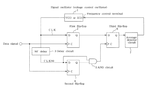
FIG. 1 is a circuit diagram for showing a
configuration of a first embodiment of the invention;
CA 02359270 2001-10-18
FIG. 2 is a timing chart for showing operations of the
first embodiment of the invention (fvco=fdata);
FIG. 3 is a timing chart for showing operations of the
first embodiment of the invention (fvco=fdata);
5 FIG. 4 is a timing chart for showing operations of the
first embodiment of the invention (fvco>fdata);
FIG. 5 is a timing chart for showing operations of the
first embodiment of the invention (fvco>fdata);
FIG. 6 is a timing chart for showing operations of the
first embodiment of the invention (fvco<fdata);
FIG. 7 is a timing chart for showing operations of the
first embodiment of the invention (fvco<fdata);
FIG. 8 is a timing chart for showing operations of the
first embodiment of the invention (with a synchronized
frequency but with a shifted phase); and
FIG. 9 is a circuit diagram for showing a configuration
of a second embodiment of the invention.
DESCRIPTION OF THE PREFERRED EMBODIMENTS
The following will describe embodiments of the
invention. One preferred embodiment of the invention has a
signal oscillator (1) comprised of a voltage control oscillator
(VCO) or a current control oscillator (ICO) which has a
frequency control terminal, for oscillating a signal
corresponding to a control voltage applied on this frequency
CA 02359270 2001-10-18
6
control terminal. A phase/frequency comparator circuit of this
embodiment includes a first flip-flop (2) for sampling an
output clock signal of the signal oscillator (1) at a trailing
or leasing edge of a receive data signal, a delay circuit (3)
for delaying the output clock signal by a predetermined phase
(90~ ), a second flip-flop (4) for sampling the clock signal
delayed by the delay circuit (3) at a trailing or leading edge
of the data signal, a logical-product circuit (5) for an output
of the second flip-flop and the clock signal (CLK90) delayed
by 90~ at the delay circuit (3) , and a third flip-flop (6) for
sampling an output of the first flip-flop at a trailing or
leading edge of an output of the logical-product circuit (5).
The phase/frequency comparator circuit of this embodiment
further includes an average detector circuit (7) for detecting
an average of outputs of the third flip-flop (6), so that an
output of the average detector circuit (7) can be fed back to
the signal oscillator (1) at its frequency control terminal to
thereby control an oscillation frequency of the signal
oscillator (1), thus causing the signal oscillator (1) to
generate a clock signal synchronized with the data signal.
Another embodiment of the invention may be of such a
configuration as shown in FIG. 9 including a latch circuit (8)
(level-sensitive latch) in place of the edge-trigger type third
flip-flop (6) . That is, in this embodiment, the latch circuit
(8) receives as an input both an output of the first flip-flop
CA 02359270 2001-10-18
7
(2) and an output of the second flip-flop (4) so that it may
provide the output, as it is, of the first flip-flop (1) when
the second flip-flop (4) outputs a first value and holds the
previous value when the second flip-flop (4) outputs a second
value, while the average detector circuit (7) detects an
average of the outputs of the latch circuit (8).
Example
To further detail the above-mentioned embodiments of
the invention, the following will describe embodiments thereof
with reference to drawings.
First Example
FIG. 1 is a circuit diagram for showing a configuration
of a first embodiment of the invention.
As shown in FIG. 1, a phase/frequency comparator circuit
of this first embodiment of the invention includes the VC01
having a f requency control terminal , the first f lip- f lop 2 for
receiving a clock signal CLK output from the VC01 at its data
terminal and a receive data signal at its clock signal terminal
C, the delay circuit 3 for delaying a clock signal output from
the VCO1 by 90~ to then output it, the second flip-flop 4 having
its data terminal D connected with an output of the delay
circuit 3 and receiving the data signal at its clock signal
terminal C, the AND circuit 5 for outputting a logical product
of an output of the second flip-flop 4 and a clock signal output
of the delay circuit 3, the third flip-flop 6 having its clock
CA 02359270 2001-10-18
8
signal terminal C connected with an output terminal of the AND
circuit 5 and its data terminal D connected with an output Q
of the first flip-flop 2, and the average detector circuit 7
for detecting and then outputting a time-wise average of the
output Q of the third flip-flop 6, in which an output (average)
of the average detector circuit 7 is fed back to the frequency
control terminal of the VCO ( 1 ) to thereby control the frequency
thereof, thus generating a clock signal synchronized with the
data signal. The first through third flip-flops 2, 4, and 6
each consist of a D-type flip-flop, which samples an input at
the data terminal D at a leading or trailing edge of the signal
at the clock signal terminal C. In this configuration, the VC01
may be replaced by an ICO for converting a voltage of the control
signal into a current based on which an oscillation frequency
thereof may be changed.
Such a circuit as shown in FIG. 1 may be used in a
reception apparatus etc. as a clock signal regenerating circuit
for regenerating a clock signal from reception data, in which
reception apparatus a light signal is converted at a
photoelectric conversion circuit such as a photodiode into an
electric signal (current) and then into a voltage, so that the
receive data signal amplified to a necessary logical amplitude
is input as the data signal in FIG. 1 to the clock signal
terminal C of the first and second flip-flop 2 and 4.
CA 02359270 2001-10-18
9
FIGS. 2-8 are timing charts for explaining the
operations of the first embodiment.
The clock signal CLK output from the VC01 is delayed by
90~ at the VC01 to provide a "CLK90"
Also, hereinafter, an oscillation frequency (frequency
of the clock signal CLK) of the VCO1 is called fvco and a basic
frequency of the receive data signal, fdata.
FIG. 2 is a timing chart for showing operations when the
frequencies are synchronized with each other, that is, when
fvco=fdata .
When the frequencies are synchronized with each other,
the leading or trailing edge of the clock signal CLK agrees with
a cross-point of the data signal always. This first embodiment
is described with reference to a case where the trailing edge
of the clock signal CLK agrees with the cross-point of the data
signal.
The first flip-flop 2 samples a transition edge of the
clock signal CLK entered at the data terminal C at a transition
edge of the data signal entered at the clock signal terminal
C. As a result, its output Q takes on a high-and-low level
random pattern due to a relationship between a set-up time and
a hold time.
The second flip-flop 4 samples the High-level VH of the
clock signal CLK90 and so its Q is at the High -level VH always.
CA 02359270 2001-10-18
Since the output Q of the second flip-flop 4 is at the
High-level, the AND circuit 5 for the output Q of the second
flip-flop 4 and CLK90 as delayed by 90~ at the delay circuit
3 outputs CLK90 as it is.
5 As shown in FIG. 3, at the clock signal terminal C of
the third flip-flop 6 is entered CLK90 delayed by 90~ at the
delay circuit 3, so that the output Q of the third flip-flop
6 receiving the output Q (high-and-low level random pattern)
of the first flip-flop 2 takes on a random pattern delayed by
10 90~ with respect to the output of the first flip-flop 2.
Accordingly, an output Vav (average voltage) of the
average detector circuit 7 for time-wise averaging the output
Q of the third flip-flop 6 takes on (VH+VL)/2, which is an
intermediate value of the HIGH-level VH and the Low-level VL.
The average detector circuit 7 provides a time-wise
average obtained by converting a High-level duration of the
output Q of the flip-flop 2 in a predetermined time period into
a DC voltage level. For example, it may be comprised of a
low-pass filter including a CR circuit having its time constant
set to a predetermined value or of a charge pump having such
a configuration that the capacitor is charged at a constant
current during a time when the output signal at the output
terminal Q of the flip-flop 2 stays at the HIGH level and, for
a period of the LOW level, is stopped in charging or discharged
so that a voltage across the capacitor at a point in time when
CA 02359270 2001-10-18
11
a predetermined time lapse has elapsed may be provided as a
time-wise average.
FIG. 4 is a timing chart for showing operations when the
clock signal frequency fvco of the VC01 is larger than the basic
frequency fdata of the data signal (fvco>fdata).
When the clock signal frequency fvco of the VC01 is
larger than the basic frequency fdata of the data signal, as
shown in FIG. 4, the cross-point of the data signal is shifted
rightward with respect to output the clock signal CLK. That
is, the data signal has a larger period than the clock signal
CLK and so its cross-point is delayed for each cycle with
respect to the transition of the trailing edge of the clock
signal CLK.
Accordingly, by the first flip-flop 2, the timing the
clock signal CLK is sampled at a variation point (transition
edge) of the data signal is delayed (shifted rightward along
the time axis in FIG. 4) for each cycle. When the HIGH-level
VH of the clock signal CLK is being sampled at the transition
edge of the data signal, the output Q of the first flip-flop
2 stays at the HIGH-level VH. When the Low-level VL of the clock
signal CLK is being sampled at the transition edge of the data
signal, on the other hand, the output Q of the first flip-flop
2 stays at the Low-level VL. Thus, the duration of the
HIGH-level VH and that of the Low-level VL of the output Q of
the first flip-flop 2 alternate with each other, so that a
CA 02359270 2001-10-18
12
frequency at which they cycle once is equal to a difference
between the frequency fdata of the data signal and the frequency
fvco of the clock signal CLK.
The output Q of the first flip-flop 2 falls always
earlier than the output of the second flip-flop 4 falls in
timing. The output Q of the first flip-flop 2 which samples
the clock signal CLK at the transition edge of the data signal
takes on the LOW level in cycle t2, while the output Q of the
second flip-flop 4 which samples CLK90 at the transition edge
of the data signal takes on the LOW level in cycle t3.
The following will describe operations of the first
embodiment of the invention in a case where the clock signal
frequency is higher than the data signal frequency (fvco>fdata)
with reference to FIG. 5. The AND circuit 5 outputs CLK90 only
when the output Q of the second flip-flop 4 is at the HIGH-
level VH. Accordingly, the output of the third flip-flop 6
takes on the High -level VH only when the outputs Q of both the
first flip-flop 2 and the second flip-flop 4 are at the
High-level VH.
When the AND circuit 5 does not output CLK90 (at the LOW
level in FIG. 5) and the clock signal is not supplied to the
clock signal terminal C of the third flip-flop 6, the third
flip-flop 6 holds its previous state.
As can be seen from FIG. 5, the output q of the first
flip-flop 2 always falls earlier than the output Q of the second
CA 02359270 2001-10-18
13
flip-flop 4 falls in timing. In other words, the output Q of
the second flip-flop 4 which samples CLK90 at the transition
edge of the data signal rises as delayed by 90~ with respect
to the output Q of the first flip-flop 2 which samples the clock
signal CLK by the data signal. Accordingly, the output Q of
the third flip-flop 6 provides a clock signal which has a
smaller duration of being at the HIGH-level VH, so that the
average detector circuit 7 outputs an intermediate value
between (VH+VL)/2 and VL (see FIG. 5).
The VC01 receives at the frequency control terminal an
average output from the average detector circuit 7 and, based
on the control signal, lowers its oscillation frequency.
Accordingly, the frequency fvco of the clock signal output from
the VC01 and the frequency fdata of the receive data agree with
each other.
FIG. 6 is a timing chart for showing operations in a case
where the clock signal frequency of the VC01 is lower than the
basic frequency fdata of the data signal (fvco<fdata).
When the frequency fvco of the clock signal CLK of the
VC01 is lower than the basic frequency fdata of the data signal,
the cross-point of the data signal is shifted leftward along
the time axis in FIG. 6 for each cycle with respect to the clock
signal CLK. That is, the clock signal CLK has a longer period
than the data signal, so that the cross-point of the data signal
CA 02359270 2001-10-18
14
advances in timing for each cycle with respect to the trailing
transition of the clock signal CLK.
Accordingly, by the first flip-flop 2, the timing the
clock signal CLK is sampled at a transition edge of the data
signal is shifted forward (leftward) along the time axis for
each cycle. That is, when the High-level VH of the clock signal
CLK is being sampled at the transition edge of the data signal,
the output Q of the first flip-flop 2 stays at the High-level
VH, whereas when the LOVJ-level VL of the clock signal CLK is
being sampled at the transition edge of the data signal, the
output Q of the first flip-flop 2 stays at the Low-level VL.
The output Q of the first flip-flop 2 becomes VH and VL levels
alternately, so that a frequency at which these two levels cycle
once is equal to a difference between the frequency fdata of
the data signal and the frequency fvco of the clock signal CLK.
Also, the output Q of the first flip-flop 2 falls always
later than the output of the second flip-flop 4 falls in timing.
The following will describe operations of a case where
the frequency of the clock signal fvco is lower than the basic
frequency of the data signal fdata (fvco<fdata) with reference
to FIG. 7. The AND circuit 5 outputs CLK90 only when the output
Q of the second flip-flop 4 is at the HIGH-level VH.
Accordingly, the output of the third flip-flop 6 takes on the
HIGH-level VH only when the outputs Q of both the first
flip-flop 2 and the second flip-flop 4 are at the HIGH-level
CA 02359270 2001-10-18
VH. When the AND circuit 5 does not output CLK90 (when the
output of the second flip-flop 4 is at the Low-level VL) , the
third flip-flop 6 holds its previous state.
As can be seen from FIG. 7, in this case, the output of
5 the first flip-flop 2 rises later by 90~ than the output of
the second flip-flop 4, so that the output of the third
flip-flop 6 provides a clock signal which has a larger duration
of being at the HIGH-level VH, which has an average between the
intermediate value of (VH+VL)/2 and the HIGH-level VH. When
10 this time-wise average is input to the VC01, the frequency fvco
of the VC01 is increased.
By controlling the VC01 so that the control voltage at
the frequency control terminal may be held at the intermediate
value of (VH+VL) /2 always, it is possible to generate the clock
15 signal CLK having the same frequency as the basic frequency of
the data signal.
The following will describe, with reference to FIGS. 1
and 8, operations of a case where the frequency fdata of the
data signal and the frequency fvco of the oscillation clock
signal of the VCO1 agree with each other but they are different
in phase, that is, the variation point of the data signal and
the leading edge of the clock signal CLK do not agree.
Fig. 8(B) is a truth table indicating a relationship
between the output of the first and second flip-flops 2 and 4
and the third flip-flop 6 and FIG. 8 (A) , a relationship among
CA 02359270 2001-10-18
16
the timing waveforms of the data signal DATA, clock signal CLK,
and clock signal CLK90 delayed at the delay circuit 3 by 90~ ,
a phase difference between the data signal DATA and the clock
signal CLK (a phase difference of 0 means phase agreement) , and
the output of the third flip-flop 6.
In the interval A (when the output Q of the first
flip-flop 2 is at the LOW level and that of the second flip-flop
4 is at the HIGH level), the output of the third flip-flop 6
takes on the LOW-level VL.
In the interval B (when the outputs Q of the first
flip-flop 2 and the second flip-flop 4 are both at the LOW
level), the third flip-flop6 holds the previous state of the
High- oz Low-level VH or VL. As can be seen from the
relationship between the phase difference between the clock
signal CLK and the data signal DATA and the output of the third
flip-flop 6 shown in FIG. 8(A), no matter whether the clock
signal CLK is ahead of or behind the data signal DATA in phase,
over a transition from the interval A to the interval B, the
third flip-flop 6 holds the Low-level output as has been in the
interval A and, over a transition from the interval B to the
interval C, holds the Low-level output as has been in the
interval B.
In the interval D (when the outputs Q of the first and
second flip-flops 2 and 4 are both at the High level), it
provides the HIGH-level output. In this case also, since an
CA 02359270 2001-10-18
17
average of the output Q of the third flip-flop 6 is different
from the intermediate value (VH+VL) /2, control is conducted so
that a time-wise average of the output Q of the third flip-
flop 6 may agree with (VH+VL) /2, thus enabling obtaining a clock
signal which is synchronized with the data signal both in
frequency and in phase.
When a transition is made from the interval D to the
interval C, the third flip-flop 6 holds the HIGH-level output
as has been in the interval D, when a transition is made from
the interval C to the interval B, it holds the HIGH-level output
as has been the interval C, and when a transition is made from
the interval B to the interval A, it provides the Low-level
output.
Thus, in the embodiment of the invention, the
relationship between a phase difference and the output of the
third flip-flop 6 which indicates a result of comparison
thereof has a hysteresis property such as shown in FIG. 8 (A) .
That is, the transition of the output of the third flip-flop
6 with respect to a detected phase (phase difference between
the clock signal CLK and the data signal DATA) has a directivity
(such as indicated by an arrow) , in other words, there is a width
(=180 ) between a phase (-270 , 90~ (=-270 +360 )) at a
transition of the output of the third flip-flop 6 from the LOW
to HIGH levels and a phase (-90~ , 270 (=-90~ +360 )) at a
transition from the HIGH to LOW levels, and, moreover, up to
CA 02359270 2001-10-18
18
an expanded phase difference range of ~270 can be detected
correctly, thus enhancing the tolerance against the noise and
fitter in the data signal.
Such a comparison example as against this embodiment may
be assumed in which a difference between the clock signal CLK
and the data signal DATA is detected by only one flip-flop
(e.g. , the second flip-flop 2 in FIG. 1) ; in this case, a phase
(~180 ) at a transition of the output of this flip-flop from
the LOW to HIGH levels agrees with a phase (~180 ) at a
transition from the HIGH to LOW levels to provide no hysteresis
property, thus enabling correctly detecting only up to a phase
difference less than ~180
Second Example
The following will describe a second embodiment of the
invention. FIG. 9 is a circuit diagram for showing a
configuration of the second embodiment of the invention. As
shown in it, in contrast to the above-mentioned embodiment,
this embodiment uses the latch circuit 8 to replace the AND
circuit 5 and the third flip-flop 6 (edge-trigger type D-
flip-flop) as its feature. The latch circuit 8 consists of a
level-sense type D-latch, acting to hold the previous state
when the clock signal terminal C is at the Low-level and output
as it is a state input at the data terminal when the clock signal
terminal is at the High-level as shown in the truth table of
FIG. 9 (B) .
CA 02359270 2001-10-18
19
The latch circuit 8 combines in operation the AND
circuit 5 and the third flip-flop 6 shown in FIG. 1. Moreover,
the latch circuit 8 can be realized in a half the circuit scale
of the third flip-flop 6, thus effectively contributing the
miniaturization and power-dissipation saving. Like the
above-mentioned embodiment, this embodiment also provides a
width between a phase at a transition from the output of the
latch circuit 8 from the LOW to HIGH levels and a phase at a
transition from the HIGH to LOW levels, thus enabling correctly
detecting a phase difference of up to ~270.
As mentioned above, the configuration of the invention
has two functions; a function to detect whether two signals are
synchronized with each other in frequency to then feed back a
detection result in the control signal to a signal oscillator
comprised of a VCO or ICO so that the two signals may agree in
frequency and another to detect a phase difference between two
signals which agreed in frequency to then feed back a detection
result in the control signal to the signal oscillator so that
they may agree in phase.
Note here that the invention may not only be applied to
a reception apparatus but also may be applied as it is as a
phase/frequency comparator circuit in a PLL circuit for
inputting a standard clock signal and outputting a signal
synchronized with this reference clock signal. That is, by
providing such a PLL circuit that, in the circuit described with
CA 02359270 2001-10-18
the above-mentioned first embodiment which includes the first
flip-flop 2, the delay circuit 3, the second flip-flop 4, the
AND circuit 5, and the third flip-flop 6 or the circuit which
includes the first flip-flop 2, the delay circuit 3, the second
5 flip-flop 4, and the latch circuit 8, an output of the third
flip-flop 6 or the latch circuit 8 respectively is smoothed into
a DC voltage by the loop filter (or the average detector circuit
7), which is in turn supplied as a control signal to the VCO,
a clock signal output from which is then directly given or
10 frequency-divided by a frequency divider circuit to provide the
clock signal CLK, which is input to the data terminal D of the
first flip-flop 2 in the phase/frequency comparator circuit
while at the same time the incoming reference signal (clock
signal) is input at the clock signal terminal C of the first
15 and second flip-flops 2 and 4, it is possible to obtain a clock
signal synchronized with the reference signal from an output
of the VCO or the frequency divider circuit.
As mentioned above, the invention gives an effect of
simplifying a circuit configuration because a phase/frequency
20 comparator circuit can be comprised of the first flip-flop
which samples a clock signal output of the VCO at a trailing
or leading edge of the data signal, the second flip-flop which
samples the clock signal output as delayed by a predetermined
phase at the trailing or leading edge of the data signal, the
third flip-flop which samples an output of the first flip-flop
CA 02359270 2001-10-18
21
at a transition edge of an AND signal obtained by AND'ing an
output of the second flip-flop and the delayed clock signal
output, and the average detector circuit which detects an
output of the third flip-flop. By the invention, it is possible
to feed back in configuration an output of the average detector
circuit to the VCO at its frequency control terminal to thereby
control an oscillation frequency of the VCO, thus generating
a clock signal synchronized with the data signal.
Also, by the invention, even when the frequency of the
data signal agrees with an oscillation frequency of the VCO but
the transition point of the data signal does not agree with a
leading or trailing edge of the clock signal in timing (that
is, the phase is shifted), phase synchronization control can
be conducted so that they may agree in phase.
Further, by the invention, it is possible to expand the
range in which a phase difference between two signals can be
detected correctly.
The invention may be embodied in other specific forms
without departing from the spirit or essential characteristic
thereof. The present embodiments are therefore to be
considered in all respects as illustrative and not restrictive,
the scope of the invention being indicated by the appended
Claims rather than by the foregoing description and all changes
which come within the meaning and range of equivalency of the
Claims are therefore intended to be embraced therein.
CA 02359270 2001-10-18
22
The entire disclosure of Japanese Patent Application
No. 2000-319748 (Filed on October 19, 2000) including
specification, claims, drawings and summary are incorporated
herein by reference in its entirety.