Note: Descriptions are shown in the official language in which they were submitted.
CA 02359386 2004-12-20
POLYANILINE AND CARBON BLACK FILLED POLYIMIDE
INTERMEDIATE TRANSFER COMPONENTS
BACKGROUND OF THE INVENTION
The present invention relates to transfer components, and more
specifically, to intermediate transfer components useful in transferring a
developed image in an electrostatographic, including xerographic and digital,
machine, from a photoreceptor or another transfer member to a copy substrate
s or another transfer member. In embodiments of the present invention, there
are
selected transfer components comprising a layer comprising electrically
conductive fillers of polyanaline and carbon black. Also, in embodiments, the
transfer member comprises a polyimide substrate. The present invention, in
embodiments, allows for the preparation and manufacture of transfer
io components with resistivity within the desired range for transfer,
resulting in
excellent electrical properties against a wide variations in transfer fields
and
enabling the transfer members to be useful at a wide variety of process
speeds.
The present invention, in embodiments, also allows for a decrease or
elimination
in pre-transfer air breakdown of the transfer member.
is In a typical electrostatographic reproducing apparatus, a light image of an
original to be copied is recorded in the form of an electrostatic latent image
upon
a photosensitive member and the latent image is subsequently rendered visible
by the application of electroscopic thermoplastic resin particles which are
commonly referred to as toner. Generally, the electrostatic latent image is
zo developed by bringing a developer mixture into contact therewith. A dry
developer mixture usually comprises carrier granules having toner particles
adhering triboelectrically thereto. Toner particles are attracted from the
carrier
granules to the latent image forming a toner powder image thereon.
Alternatively, a liquid developer material may be employed. The liquid
developer
2s material includes a liquid carrier having toner particles dispersed
therein. The
1
CA 02359386 2001-10-22
liquid developer material is advanced into contact with the electrostatic
latent
image and the toner particles are deposited thereon in image configuration.
After the toner particles have been deposited on the photoconductive surface,
in
image configuration, they are transferred to a copy sheet. However, when a
s liquid developer material is employed, the copy sheet is wet with both the
toner
particles and the liquid carrier. Thus, it is necessary to remove the liquid
carrier
from the copy sheet. This may be accomplished by drying the copy sheet prior
to fusing of the toner image, or relying upon the fusing process to
permanently
fuse the toner particles to the copy sheet as well as vaporizing the liquid
carrier
to adhering thereto. However, it is desirable to refrain from transferring any
liquid
carrier to the copy sheet. Therefore, it is advantageous to transfer the
developed image to an intermediate transfer component, and subsequently
transfer with very high transfer efficiency, the developed image from the
intermediate transfer component to a permanent substrate. The toner image is
is usually fixed or fused upon a support which may be the photosensitive
member
itself or other support sheet such as plain paper.
In an alternative reproducing apparatus, marking material may be
deposited image-wise onto a first image-bearing member. This marking material
is then transferred onto a second image-bearing apparatus such as an
2o intermediate transfer member in accordance with an embodiment of this
invention. Subsequently, the marking material may be transferred onto a third
image-bearing member, typically the final copy sheet, such as paper,
transparency, or the like. The marking material of this alternative
reproducing
apparatus may include a waxy material that is melted and projected onto the
first
2s image bearing member, dry toner particles that are electostatically or
acoustically
projected onto the first image bearing member, or liquid toner that is
partially
dried as it is projected from an orifice to the first image bearing member.
The
marking material may be charged before, during, or after its deposition onto
the
first image bearing apparatus. The transfers to the second and third image
3o bearing members may use electric fields, differential adhesion and/or the
like.
2
CA 02359386 2001-10-22
This invention provides controlled resistivity for the second image-bearing
member and this controlled resistivity is especially beneficial in electric
field
induced transfer.
U.S. Patent 5,298,956 to Mammino et al. discloses a seamless
s intermediate transfer member. Polyimide is listed as a possible layer for
the
intermediate transfer member. A polymer filler such as polyanaline is also
disclosed.
U.S. Patent 5,876,636 to Schlueter, Jr. et al. discloses haloelastomer and
doped metal oxide compositions. The compositions are disclosed as being
io useful as layers in xerographic components. Polyanaline and carbon black
fillers
are given as examples of conductive fillers.
U.S. Patent 5,995,796 to Schlueter, Jr. et al. discloses haloelastomer and
doped metal oxide film components useful in xerographic processes.
Polyanaline and carbon black fillers are given as examples of conductive
fillers.
is In scalable tandem color marking, charged toner particles are transferred
first to an intermediate transfer belt and then to a final substrate. Some
transfers
use electric fields to transfer the toner particles. In other machines, the
first
transfer is electrostatic and the second transfer can combine transfer and
fixing.
For a given applied voltage, for example on a bias transfer member, the
2o electrical resistivity of an intermediate transfer member determines the
voltage
drop across the intermediate transfer member and the field acting on the toner
particles. A small range of resistivity is desired to give the high transfer
fields
without pre-transfer air breakdown. It is difficult to manufacture a material
transfer layer having this narrow resistivity.
2s Attempts at achieving this narrow resistivity have led to loading an
elastomer transfer substrate with conducting particles. However, this loading
typically leads to a large decrease in resistivity when the loading reaches a
value
called a percolation threshold. The rapid change of resistivity near the
percolation threshold makes it difficult to reproducibly manufacture material
with
3o the desired resistivity. Small changes in particle concentration, in
particle
3
CA 02359386 2001-10-22
morphology, in particle surface chemistry, or in particle aggregation into
larger
aggregates, cause large changes in resistivity.
A very conductive intermediate transfer member is not desirable because
the high transfer fields cause arcing at the charge deficient spots on the
s photoconductor. In addition, a very conductive intermediate transfer member
results in high pre-transfer fields that cause air breakdown and toner
discharge
prior to transfer. Conversely, a very insulating intermediate transfer member
is
not desirable because the result is a large voltage drop across the
intermediate
transfer member and only a weak field to transfer toner.
io Therefore, it is desirable to provide an intermediate transfer member that
has a volume resistivity within a desired range necessary for sufficient
transfer of
toner within a wide variety of process speeds. It is further desirable to
provide an
intermediate transfer member that possesses a wide latitude against variations
in
the transfer field.
is Attempts at making such a semi-insulating intermediate transfer member
having the above desired characteristics have been difficult. Attempts focused
on using an insulating plastic or elastomer loaded with conducting particles
or
with ionic conductors. Control of volume resistivity by loading with ionic
conductors is difficult because changes in relative humidity generally lead to
2o changes in resistivity. Sometimes this occurs as soon as the relative
humidity
changes and sometimes it occurs only after prolonged printing at an extreme
corner of the print engine's environmental window (i.e., the range of
temperatures and humidities at which the print engine operates).
Therefore, there is still a need for a semi-insulating intermediate transfer
2s member which can be used for transferring a toner image across a wide
variety
of process speeds, and that possesses a wide latitude against variations in
the
transfer field.
SUMMARY OF THE INVENTION
4
CA 02359386 2004-12-20
Embodiments of the present invention include: a transfer member
having a substrate comprising a polyimide having polyaniline and carbon
black electrically conductive fillers dispersed therein.
In addition, embodiments include: an image forming apparatus for
forming images on a recording medium comprising: a charge-retentive
surface to receive an electrostatic latent image thereon; a development
component to apply toner to the charge-retentive surface to develop the
electrostatic latent image to form a developed image on the charge retentive
surface; a transfer component to transfer the developed image from the
charge retentive surface to a copy substrate, the transfer member having a
substrate comprising a polyimide having polyaniline and carbon black
electrically conductive fillers dispersed in the substrate.
Moreover, embodiments include: a transfer member comprising a
substrate comprising a polyimide having from about 5 to about 25 percent by
weight of total solids polyaniline, and from about 1 to about 10 percent by
weight of total solids carbon black electrically conductive fillers dispersed
therein, wherein the transfer member has an electrical volume resistivity of
from about 10' to about 103 ohm-cm.
According to an aspect of the present invention, there is provided a
transfer member having a substrate comprising a polyimide having polyaniline
fillers, graphite fillers, and carbon black fillers other than graphite
fillers
dispersed in the substrate.
According to another aspect of the present invention, there is provided
an image forming apparatus for forming images on a recording medium
comprising: a charge-retentive surface to receive an electrostatic latent
image
thereon; a development component to apply toner to the charge-retentive
surface to develop the electrostatic latent image to form a developed image
on the charge retentive surface; a transfer member to transfer the developed.
image from the charge retentive surface to a copy substrate, the transfer
member comprising a substrate comprising a polyimide having polyaniline,
graphite and carbon black other than graphite fillers dispersed in the
substrate.
5
CA 02359386 2004-12-20
According to a further aspect of the present invention, there is provided
a transfer member comprising a substrate comprising a polyimide having from
about 5 to about 25 percent by weight of total solids polyaniline and from
about 1 to about 10 percent by weight to total solids carbon black dispersed
therein, wherein the transfer member has an electrical volume resistivity of
from about 10' to about 10'3 ohm-cm.
BRIEF DESCRIPTION OF THE DRAWINGS
For a better understanding of the present invention, reference may be
had to the accompanying figures.
Figure 1 is a schematic illustration of an image apparatus in
accordance with the present invention.
Figure 2 is an illustration of an embodiment of the present invention,
and represents a transfix member.
Figure 3 is a schematic view of an image development system
containing an intermediate transfer member.
5a
CA 02359386 2001-10-22
Figure 4 is an illustration of an embodiment of the invention, wherein a
two layer transfer film comprising a substrate and an outer layer as described
herein is shown.
Figure 5 is an illustration of an embodiment of the invention, wherein a
s three layer transfer film having a substrate, an intermediate layer and an
outer
layer as described herein is shown.
Figure 6 is an illustration of an embodiment of the invention and
demonstrates a transfer member having both carbon black and polyanaline
electrically conductive fillers dispersed in the substrate.
Figure 7 is a graph of volume resistivity versus carbon black content for
polyimide films containing about 15 weight percent polyanaline.
Figure 8 is a graph showing environmental dependence of volume
resistivity versus applied voltage for a preferred embodiment of the invention
of a
polyimide substrate with about 15 percent polyanaline and about 4.9 percent
carbon black.
DETAILED DESCRIPTION OF THE PRESENT INVENTION
io The present invention relates to transfer members comprising a polyimide
substrate having electrically conductive fillers dispersed or contained
therein. In
an embodiment, the electrically conductive fillers comprise polyanaline and
carbon black fillers. In a preferred embodiment, the polyimide substrate
comprises both carbon black and polyanaline electrically conductive fillers.
The
is transfer member may comprise an outer layer on the substrate, and may also
comprise an intermediate layer between the outer layer and the substrate.
Referring to Figure 1, in a typical electrostatographic reproducing
apparatus, a light image of an original to be copied is recorded in the form
of an
electrostatic latent image upon a photosensitive member and the latent image
is
2o subsequently rendered visible by the application of electroscopic
thermoplastic
resin particles which are commonly referred to as toner. Specifically,
6
CA 02359386 2001-10-22
photoreceptor 10 is charged on its surface by means of a charger 12 to which a
voltage has been supplied from power supply 11. The photoreceptor is then
imagewise exposed to light from an optical system or an image input apparatus
13, such as a laser and light emitting diode, to form an electrostatic latent
image
s thereon. Generally, the electrostatic latent image is developed by bringing
a
developer mixture from developer station 14 into contact therewith.
Development can be effected by use of a magnetic brush, powder cloud, or other
known development process. A dry developer mixture usually comprises carrier
granules having toner particles adhering triboelectrically thereto. Toner
particles
to are attracted from the carrier granules to the latent image forming a toner
powder
image thereon. Alternatively, a liquid developer material may be employed,
which includes a liquid carrier having toner particles dispersed therein. The
liquid developer material is advanced into contact with the electrostatic
latent
image and the toner particles are deposited thereon in image configuration.
is After the toner particles have been deposited on the photoconductive
surface, in image configuration, they are transferred to a copy sheet 16 by
transfer means 15, which can be pressure transfer or electrostatic transfer.
Alternatively, the developed image can be transferred to an intermediate
transfer
member, or bias transfer member, and subsequently transferred to another
2o transfer member or to a copy sheet. Examples of copy substrates include
paper,
transparency material such as polyester, polycarbonate, or the like, cloth,
wood,
or any other desired material upon which the finished image will be situated.
After the transfer of the developed image is completed, copy sheet 16
advances to fusing station 19, depicted in Figure 1 as fuser roll 20 and
pressure
2s roll 21 (although any other fusing components such as fuser belt in contact
with
a pressure roll, fuser roll in contact with pressure belt, and the like, are
suitable
for use with the present apparatus), wherein the developed image is fused to
copy sheet 16 by passing copy sheet 16 between the fusing and pressure
members, thereby forming a permanent image. Alternatively, transfer and fusing
3o can be effected by a transfix application. In the transfix application, the
marking
CA 02359386 2001-10-22
material can be, in preferred embodiments, softened by heating before and/or
during transfer to the final image receiving medium. In this manner, the image
is
fixed to the final image-receiving medium by cooling after transfer and a
later
fusing step is eliminated.
Photoreceptor 10, subsequent to transfer, advances to cleaning station
17, wherein any toner left on photoreceptor 10 is cleaned therefrom by use of
a
blade (as shown in Figure 1 ), brush, or other cleaning apparatus.
The transfer members employed for the present invention can be of any
io suitable configuration. Examples of suitable configurations include a
sheet, a
film, a web, a foil, a strip, a coil, a cylinder, a drum, an endless mobius
strip, a
circular disc, a belt including an endless belt, an endless seamed flexible
belt,
an endless seamless flexible belt, an endless belt having a puzzle cut seam,
and the like.
is The transfer components of the instant invention may be employed in
either an image on image transfer or a tandem transfer of a toned images) from
the photoreceptor to the intermediate transfer component, or in a transfix
system for simultaneous transfer and fusing the transferred and developed
latent image to the copy substrate. In an image on image transfer, the color
2o toner images are first deposited on the photoreceptor and all the color
toner
images are then transferred simultaneously to the intermediate transfer
component. In a tandem transfer, the toner image is transferred one color at a
time from the photoreceptor to the same area of the intermediate transfer
component.
2s Transfer of the developed image from the imaging member to the
intermediate transfer element and transfer of the image from the intermediate
transfer element to a copy substrate can be by any suitable technique
conventionally used in electrophotography, such as corona transfer, pressure
transfer, bias transfer, and combinations of those transfer means, and the
like.
3o In the situation of transfer from the intermediate transfer medium to the
a
CA 02359386 2001-10-22
substrate, transfer methods such as adhesive transfer, wherein the receiving
substrate has adhesive characteristics with respect to the developer material,
can also be employed. Typical corona transfer entails contacting the deposited
toner particles with the substrate and applying an electrostatic charge on the
s surface of the substrate opposite to the toner particles. A single wire
corotron
having applied thereto a potential of between about 5,000 and about 8,000
volts
provides satisfactory transfer. In a specific process, a corona generating
device
sprays the back side of the image receiving member with ions to charge it to
the
proper potential so that it is tacked to the member from which the image is to
be
1o transferred and the toner powder image is attracted from the image bearing
member to the image receiving member. After transfer, a corona generator
charges the receiving member to an opposite polarity to detach the receiving
member from the member that originally bore the developed image, whereupon
the image receiving member is separated from the member that originally bore
is the image.
For color imaging, typically, four or more image forming devices are used,
one for each color to be printed. The colors may be cyan, magenta, yellow and
black, or may be a hexachrome set of process colors, and may also include one
or more spot colors, and/or a varnish. The image forming devices may each
2o comprise an image receiving member in the form of a photoreceptor of other
image receiving member. The intermediate transfer member of an embodiment
of the present invention is supported for movement in an endless path such
that
incremental portions thereof move past the image forming components for
transfer of an image from each of the image receiving members. Each image
2s forming component is positioned adjacent the intermediate transfer member
for
enabling sequential transfer of different color toner images to the
intermediate
transfer member in superimposed registration with one another.
The intermediate transfer member moves such that each incremental
portion thereof first moves past an image forming component and comes into
3o contact with a developed color image on an image receiving member. A
9
CA 02359386 2004-12-20
transfer device, which can comprise a corona discharge device, serves to
effect
transfer of the color component of the image at the area of contact between
the
receiving member and the intermediate transfer member. In a like fashion,
image components of colors such as red, blue, brown, green, orange, magenta,
s cyan, yellow and black, corresponding to the original document also can be
formed on the intermediate transfer member one color on top of the other to
produce a full color image.
A transfer sheet or copy sheet is moved into contact with the toner image
on the intermediate transfer member. A bias transfer member may be used to
io provide good contact between the sheet and the toner image at the transfer
station. A corona transfer device also can be provided for assisting the bias
transfer member in effecting image transfer. These imaging steps can occur
simultaneously at different incremental portions of the intermediate transfer
member. Further details of the transfer method employed herein are set forth
in
is U.S. Patent 5,298,956 to Mammino.
The intermediate transfer member herein can be employed in various
devices including, but not limited to, devices described in U.S. Patent Nos.
3,893,761; 4,531,825; 4,684,238; 4,690,539; 5,119,140; and 5,099,286.
Transfer and fusing may occur simultaneously in a transfix configuration.
2o As shown in Figure 2, a transfer apparatus 15 is depicted as transfix belt
4 being
held in position by driver rollers 22 and heated roller 2. Heated roller 2
comprises
a heater element 3. Transfix belt 4 is driven by driving rollers 22 in the
direction
of arrow 8. The developed image from photoreceptor 10 (which is driven in
direction 7 by rollers 1 ) is transferred to transfix belt 4 when contact with
2s photoreceptor 10 and belt 4 occurs. Pressure roller 5 aids in transfer of
the
developed image from photoreceptor 10 to transfix belt 4. The transferred
image
is subsequently transferred to copy substrate 16 and simultaneously fixed to
copy substrate 16 by passing the copy substrate 16 between belt 4
io
CA 02359386 2004-12-20
(containing the developed image) and pressure roller 9 in the direction of
arrow
6. A nip is formed by heated roller 2 with heating element 3 contained therein
and pressure roller 9. Copy substrate 16 passes through the nip formed by
heated roller 2 and pressure roller 9, and simultaneous transfer and fusing of
the
s developed image to the copy substrate 16 occurs.
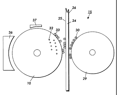
Figure 3 demonstrates another embodiment of the present invention and
depicts a transfer apparatus 15 comprising an intermediate transfer member 24
positioned between an imaging member 10 and a transfer roller 29. The imaging
member 10 is exemplified by a photoreceptor drum. However, other appropriate
io imaging members may include other electrostatographic imaging receptors
such
as ionographic belts and drums, electrophotographic belts, and the like.
In the multi-imaging system of Figure 3, each image being transferred is
formed on the imaging drum by image forming station 36. Each of these images
is then developed at developing station 37 and transferred to intermediate
is transfer member 24. Each of the images may be formed on the photoreceptor
drum 10 and developed sequentially and then transferred to the intermediate
transfer member 24. In an alternative method, each image may be formed on
the photoreceptor drum 10, developed, and transferred in registration to the
intermediate transfer member 24. In a preferred embodiment of the invention,
the
2o multi-image system is a color copying system. In this color copying system,
each
color of an image being copied is formed on the photoreceptor drum. Each color
image is developed and transferred to the intermediate transfer member 24. As
above, each of the colored images may be formed on the drum 10 and
developed sequentially and then transferred to the intermediate transfer
member
2s 24. In the alternative method, each color of an image may be formed on the
photoreceptor drum 10, developed, and transferred in registration to the
intermediate transfer member 24. .
After latent image forming station 36 has formed the latent image on the
photoreceptor drum 10 and the latent image of the photoreceptor has been
3o developed at developing station 37, the charged toner particles 33 from the
a
CA 02359386 2001-10-22
developing station 37 are attracted and held by the photoreceptor drum 10
because the photoreceptor drum 10 possesses a charge 32 opposite to that of
the toner particles 33. In Figure 3, the toner particles are shown as
negatively
charged and the photoreceptor drum 10 is shown as positively charged. These
s charges can be reversed, depending on the nature of the toner and the
machinery being used.
A biased transfer roller 29 positioned opposite the photoreceptor drum 10
has a higher voltage than the surface of the photoreceptor drum 10. As shown
in Figure 3, biased transfer roller 29 charges the backside 26 of intermediate
to transfer member 24 with a positive charge. In an alternative embodiment of
the
invention, a corona or any other charging mechanism may be used to charge the
backside 26 of the intermediate transfer member 24.
The negatively charged toner particles 33 are attracted to the front side 25
of the intermediate transfer member 24 by the positive charge 30 on the
is backside 26 of the intermediate transfer member 24.
The intermediate transfer member may be in the form of a sheet, web or
belt as it appears in Figure 3, or in the form of a roller or other suitable
shape. In
a preferred embodiment of the invention, the intermediate transfer member is
in
the form of a belt. In another embodiment of the invention, not shown in the
2o figures, the intermediate transfer member may be in the form of a sheet.
Figure 4 demonstrates a two-layer configuration of an embodiment of the
present invention. Included therein is a substrate 40 and outer layer 41.
Preferably, the substrate is comprised of a suitable high elastic modulus
material such as a polyimide material. The material should be capable of
2s becoming conductive upon the addition of electrically conductive particles.
A
polyimide having a high elastic modulus is preferred because the high elastic
modulus optimizes the stretch registration and transfer conformance. The
polyimide used herein has the advantages of improved flex life and image
registration, chemical stability to liquid developer or toner additives,
thermal
3o stability for transfix applications and for improved overcoating
manufacturing,
12
CA 02359386 2001-10-22
improved solvent resistance as compared to known materials used for film for
transfer components.
Suitable polyimides include those formed from various diamines and
dianhydrides, such as poly(amide-imide), polyetherimide, siloxane
s polyetherimide block copolymer such as, for example, SILTEM STM-1300
available from General Electric, Pittsfield, Massachusetts, and the like.
Preferred polyimides include those sold under the name KAPTON°
from
DuPont, and aromatic polyimides such as those formed by the reacting
pyromellitic acid and diaminodiphenylether sold under the tradename
to KAPTON~-type-HN, available from DuPont. Another suitable polyimide
available from DuPont and sold as KAPTON°-Type-FPC-E, is produced by
imidization of copolymeric acids such as biphenyltetracarboxylic acid and
pyromellitic acid with two aromatic diamines such as p-phenylenediamine and
diaminodiphenylether. Another suitable polyimide includes pyromellitic
is dianhydride and benzophenone tetracarboxylic dianhydride copolymeric acids
reacted with 2,2-bis[4-(8-aminophenoxy) phenoxy]-hexafluoropropane available
as EYMYD type L-20N from Ethyl Corporation, Baton Rouge, Louisiana. Other
suitable aromatic polyimides include those containing 1,2,1',2'-
biphenyltetracarboximide and para-phenylene groups such as UPILEX°-S
zo available from Uniglobe Kisco, Inc., White Planes, New York, and those
having
biphenyltetracarboximide functionality with diphenylether end spacer
characterizations such as UPILEX~-R also available from Uniglobe Kisco, Inc.
Mixtures of polyimides can also be used.
The polyimide is present in the film in an amount of from about 65 to
2s about 94 percent by weight of total solids, preferably from about 79 to
about 87
percent by weight of total solids. Total solids as used herein includes the
total
percentage by weight of polymer, conductive fillers and any additives in the
layer.
It is preferred that the polyimide contain electrically conductive fillers of
3o two kinds. One kind of preferred filler is an organic polymeric filler such
as, for
13
CA 02359386 2001-10-22
example, polyanaline, polypyrrole, polythiophene, polyacetylene, and the like.
A
particularly preferred organic filler is a polyanaline filler. The organic
filler is
present in the substrate in an amount of from about 5 to about 25 and
preferably
from about 10 to about 15 percent by weight of total solids.
s The second kind of preferred filler is a conventional electrically
conductive particulate material filler such as, for example, carbon fillers
such as
carbon black, graphite and the like; doped metal oxide such as doped tin oxide
and the like; metals such as copper, iron, magnesium, calcium and the like;
and
metal oxides such as iron oxide, copper oxide, magnesium dioxide, calcium
to hydroxide, and the like.
In a preferred embodiment, the particulate filler is a carbon filler.
Examples of suitable carbon fillers include carbon black, graphite,
fluorinated
carbon, and the like. The carbon filler is present in the substrate in an
amount
of from about 1 to about 10, and preferably from about 3 to about 6 percent by
is weight of total solids.
Carbon black systems can be established to make polymers conductive.
By use of a combination of carbon blacks as disclosed herein, the conductivity
of
a polymer can be tailored to a desired conductivity which is unexpectedly
higher
(resistance unexpectedly lower) than what would be expected. For example, the
2o inventors have demonstrated that by dispersing graphite in a polymer layer
(e.g.,
fluoroelastomer, 4.5 by 9 inches), the resistance of the layer is about 30
ohms.
By dispersing a non-graphite carbon black such as BLACK PEARL°
2000 in a
polymer (e.g., fluoroelastomer, 4.5 by 9 inches), the resistance of the layer
was
determined to be 1270 ohms. By combining a mixed carbon black system
2s comprising a graphite carbon black and a non-graphite carbon black, and
dispersing the mixed carbon black system into a polymer, the inventors found
the
resistance of the layer to be 10 ohms, which is unexpectedly lower than both
conductivities.
The phrase "more than one variety of carbon black" or "carbon black of a
3o different variety" as used herein, refers to using carbon blacks with
different
14
CA 02359386 2001-10-22
particle geometries, carbon blacks with different resistivities or
conductivities,
carbon blacks with different chemistries, carbon blacks with different surface
additives, andlor carbon blacks with different particle sizes. The use of such
carbon systems provides a coating with controlled conductivity within a
desired
s resistivity range that is virtually unaffected by changes in temperature,
relative
humidity and relatively small changes in filler loadings. Also, resistive
heating
layers using carbon systems as defined herein provide greater thickness
control
and coating consistency.
In a preferred embodiment, a graphite carbon black is used in
io combination with a carbon black that is other than graphite, i.e., a non-
graphite
carbon black. Graphite carbon black is defined as being of crystalline shape,
or
the crystalline allotropic form of carbon black, and non-graphite carbon black
is a
finely divided form of carbon black. In graphite, carbon atoms are located in
a
plane of symmetrical hexagons and there are layers and layers of these planes
is in graphite. Non-graphite carbon black, as used herein, refers to any
carbon
black which is not of crystalline allotropic form. Non-graphite carbon black
is
formed by incomplete combustion of organic substances, such as hydrocarbons.
Examples of non-graphite carbon blacks include furnace blacks, channel blacks,
thermal blacks, lamp blacks, acetylene blacks, and the like. Structurally, non-
2o graphite carbon blacks consist of bundles of parallel orientated graphite
planes
at a distance of between 3.5 to 3.8 angstroms.
Another preferred mixture of carbon black comprises a carbon black or
graphite having a particle shape of a sphere, flake, platelet, fiber, whisker,
or
rectangle used in combination with a carbon black or graphite with a different
2s particle shape, to obtain optimum filler packing and thus optimum
conductivities.
For example, a graphite having a crystalline shape can be used with a non-
graphite carbon black having a shape other than a crystalline shape.
Similarly, by use of relatively small particle size non-graphite carbon
blacks with relatively large particle size graphite, the smaller particles
"fit" into the
3o packing void areas of the resistive heating layer to improve particle
touching. As
is
CA 02359386 2004-12-20
an example, a graphite carbon black having a relatively large particle size of
from
about micron 0.1 micron to about 100 microns, preferably from about 2 to about
microns, and particularly preferred of from about 5 to about 10 microns, can
be used in combination with a non-graphite carbon black having a relatively
small
s particle size of from about 10 nanometers to about 1 micron, preferably from
about 10 nanometers to about 100 nanometers, and particularly preferred from
about 10 nanometers to about 80 nanometers.
In another preferred embodiment, it is preferred to mix a first graphite
carbon black having a bulk resistivity of from about 10° to about 10-5
ohms-cm,
to and preferably from about 10'' to about 10'° ohms-cm, with a second
non
graphite conductive carbon black having a bulk resistivity of from about
10° to
about 10'Z ohms-cm, and preferably from about 102 to about 10'' ohms-cm.
A first, preferably graphite, carbon black in an amount of from about 5 to
about to about 80, and preferably from about 25 to about 75 percent by weight
of
is a second, preferably non-graphite, carbon black frller, is preferably used
in
combination with a second conductive carbon black in an amount of from about
1 to about 30, and preferably from about 3 to about 20 percent by weight of
the
first carbon black filler.
Examples of suitable carbon blacks useful herein include those non-
2o graphite carbon blacks such as KETJEN BLACK° from ARMAK Corp;
VULCAN°
XC72, VULCAN° XC72, BLACK PEARLS° 2000, and REGAL°
2508 available
from Cabot Corporation Special Blacks Division; THERMAL BLACK° from RT
Van Derbilt, Inc.; Shawinigan Acetylene Blacks available from Chevron Chemical
Company; furnace blacks; ENSACO° Carbon Blacks and THERMAX Carbon
2s Blacks available from R.T. Vanderbilt Company, Inc.; those graphites
available
from Southwestern Graphite of Burnet, Texas, GRAPHITE 56-55 (10 microns,
10'' ohm/sq), Graphite FP 428J from Graphite Sale, Graphite 2139, .2939 and
5535 from Superior Graphite, and Graphites M450 and HPM850 from Asburry,
and ACCUFLUOR~ 2028 and ACCUFLUOR° 2010 available from Allied Signal,
3o Morristown, New Jersey.
16
CA 02359386 2001-10-22
In a particularly preferred embodiment of the invention, a preferred
mixture of carbon black comprises non-graphite carbon black such as BLACK
PEARL~ 2000 which has a nitrogen surface area of 1500 m2/g, an oil absorption
of 300 cc/100g, a non-crystalline shape, a particle size of 12 manometers, and
a
s density of 9 Ibs/ft3, used in combination with a graphite carbon black
having a
density of from about 1.5 to about 2.25 Ibs/ft3, a coefficient of friction of
about
0.1 p, a crystalline shape, and a particle size of about 10 microns.
Turning now to embodiments of the invention involving layer
configurations, Figure 4 demonstrates an embodiment of the invention and
io depicts polyimide substrate 40 and outer layer 41.
Figure 6 demonstrates an alternative embodiment of the invention and
depicts polyimide film 40 having electrically conductive fillers 43 (carbon
black)
and 44 (polyanaline) dispersed or contained within the polyimide film 40.
In another embodiment of the invention, the transfer member is of a three-
is layer configuration as shown in Figure 5. In this three layer
configuration, the
transfer member comprises a polyimide substrate 40 as defined above, and
having thereon an adhesive layer 42 positioned on the substrate, and an outer
release layer 41 positioned on the intermediate layer. The three-layer
configuration works very well with liquid development.
2o Preferred outer release layers 41 (Figures 4 and 5) include low surface
energy materials such as TEFLON°-like materials including fluorinated
ethylene
propylene copolymer (FEP), polytetrafluoroethylene (PTFE), perfluoroalkoxy
tetrafluoroethylene (PFA TEFLON°) and other TEFLON°-like
materials; silicone
materials such as fluorosilicones and silicone rubbers such as Silicone Rubber
2s 552, available from Sampson Coatings, Richmond, Virginia, (polydimethyl
siloxane/dibutyl tin diacetate, 0.45 g DBTDA per 100 grams polydimethyl
siloxane rubber mixture, with molecular weight of approximately 3,500); and
fluoroelastomers such as those sold under the tradename VITON° such as
copolymers and terpolymers of vinylidenefluoride, hexafluoropropylene and
3o tetrafluoroethylene, which are known commercially under various
designations
m
CA 02359386 2001-10-22
as VITON A~, VITON E~, VITON E60C~, VITON E45~, VITON E430°, VITON B
910~, VITON GH~, VITON B50~, VITON E45°, and VITON GF°. The
VITON°
designation is a Trademark of E.I. DuPont de Nemours, Inc. Two preferred
known fluoroelastomers are (1 ) a class of copolymers of vinylidenefluoride,
s hexafluoropropylene and tetrafluoroethylene, known commercially as
VITON° A,
(2) a class of terpolymers of vinylidenefluoride, hexafluoropropylene and
tetrafluoroethylene known commercially as VITON B~, and (3) a class of
tetrapolymers of vinylidenefluoride, hexafluoropropylene, tetrafluoroethylene
and
a cure site monomer such as VITON GF° having 35 mole percent of
io vinylidenefluoride, 34 mole percent of hexafluoropropylene and 29 mole
percent
of tetrafluoroethylene with 2 percent cure site monomer. The cure site monomer
can be those available from DuPont such as 4-bromoperfluorobutene-1, 1,1-
dihydro-4-bromopertluorobutene-1, 3-bromoperfluoropropene-1, 1,1-dihydro-3
bromoperfluoropropene-1, or any other suitable, known, commercially available
is cure site monomer.
Preferred adhesive layers 42 (Figure 5) include silanes, epoxies and other
known adhesives.
The adhesive layer and/or the outer release layer may also comprise a
filler such as carbon black, graphite, polymer fillers, metal fillers, metal
oxide
2o fillers, and/or doped metal oxide fillers.
Additives can be added to the intermediate transfer member. More
specifically, a compatibilizer, wetting agent and/or a conductivity modifyer
can be
added. Such agents can be added to help disperse the carbon black, to adjust
the chemical interaction between the carbon black and the host polymer, and/or
Zs to control the resistivity of the polyanaline. For example, the carbon
black
surface may be fluorinated (as it is in ACCUFLUOR° 2028 and
ACCUFLUOR°
2010) to help dispersion and modify its resistivity. As another example,
phosphoric acid can be added to polyanaline to control its conductivity.
The volume resistivity of the transfer member is from about 10' to about
30 10'3, and preferably about 109 to about 10" ohm-cm. This narrow range of
i$
CA 02359386 2004-12-20
resistivity is semi-insulating and allows for sufficient transfer of a toner
image
across a wide range of process speeds, without the drawbacks too high
conductivity or too much insulation. Specifically, within this narrow range of
resistivity, arcing at charge deficient spots and high pre-transfer fields
causing air
s breakdown and toner discharge prior to transfer are both reduced and/or
eliminated. Further, with a semi-insulating intermediate transfer member, a
large
voltage drop across the intermediate transfer member and a weak field to
transfer toner is also reduced and/or eliminated. Moreover, with the present
semi-insulating intermediate transfer member, drastic and/or immediate changes
to in resistivity resulting from changes in relative humidity are reduced
and/or
eliminated.
The circumference and width of the component in a film or belt
configuration of from 1 to 4 or more layers will depend on the architecture of
the
print engine in which it is used. The circumference in typical four color
print
is engines is from about 8 to about 120 inches, preferably from about 10 to
about
110 inches, and particularly preferred from about 44 to about 110 inches. The
width of the film or belt is from about 8 to about 40 inches, preferably from
about
to about 36 inches, and particularly preferred from about 10 to about 30
inches. It is preferable that the film be an endless, seamless flexible belt
or a
2o seamed flexible belt, which may or may not include puzzle cut seam(s).
Examples of such belts are described in U.S. Patent Numbers 5,487,707;
5,514,436; and Japanese Patent Application No. 8066974 filed August 29, 1994.
A method for manufacturing reinforced seamless belts is set forth in U.S.
Patent
5,409,557. Other techniques which can also be used for fabricating films or
belts
25 include ultrasonic or impulse welding.
In other machine architectures, it may be advantageous the use a transfer
member in the form of a roll. It will be understood that the preferred
embodiment
involving a combination of polymer host matrix, polyaniline, and one or more
19
CA 02359386 2001-10-22
carbon black species can be used for such rolls. In a preferred invention, the
combination of polymer host matrix, polyanaline and one or more carbon black
species would be used as a coating on a conducting cylinder which may be
grounded or biased.
s In an embodiment comprising outer layers, or intermediate and outer
layers, the layer or layers may be deposited on the substrate via well-known
coating processes. Known methods for forming the outer layers) on the
substrate film such as dipping, spraying such as by multiple spray
applications of
very thin films, casting, flow-coating, web-coating, roll-coating, extrusion,
io molding, or the like can be used. It is preferred to deposit the layers by
spraying
such as by multiple spray applications of very thin films, casting, by web
coating,
by flow-coating and most preferably by laminating.
The thickness of the substrates or coatings as described herein is from
about 2 microns to about 200 microns. When polyimide is used as the host
is polymer, its high strength enables a thinner belt such as, for example from
about
50 to about 150 microns, and preferred of from about 75 to about 100 microns.
The following Examples further define and describe embodiments of the
present invention. Unless otherwise indicated, all parts and percentages are
by
weight.
CA 02359386 2001-10-22
Measuring Surface Resistivity
The surface resistivity was measured with a Hiresta IP meter and an HR
probe. This probe consisted of an outer ring electrode (30 mm inner diameter)
and an inner disk electrode (16 mm diameter). A belt sample was placed on a
nonconducting surface and the probe was placed on top of the sample. A
voltage was applied to the ring electrode and the current from the disk
electrode
was measured. The surface resistivity in ohms/square was calculated from
voltage and current. The volume resistivity was measured by first evaporating
gold electrodes, 3/8" in diameter and approximately 100 nm thick on opposite
sides of the belt material. A voltage was applied to one electrode. The
current
from the opposite electrode was then measured. The volume resistivity in ohm-
cm was calculated from voltage current, sample thickness and gold electrode
area.
The Percolation Threshold
The data shown in Tables I and II for VITON~ fluoroelastomer films
containing various carbon black loadings, demostrates the percolation
threshold
usually present with carbon loaded polymers. For coated films of VITON~ loaded
with carbon black (the carbon black is not subjected to fluorination), the
lateral
resistivity decreases by about eight orders of magnitude as carbon black
loading
increases from 0 to 2 percent. For blade-coated films of VITON~ loaded with
ACCUFLUOR~ 2010 (fluorinated carbon black), the resistivity decreases about
eight orders of magnitude as the carbon black loading increases from 2 percent
to 5 percent. For spray-coated films of VITON~ loaded with ACCUFLUOR~ 2010
(fluorinated carbon black) the decrease in resistivity does not start until
the
carbon black exceeds 5 percent, and then the resistivity decreases 7 orders of
21
CA 02359386 2001-10-22
magnitude as the carbon black loading increases from 5 percent to 10 percent.
Only the particular case of ACCUFLUOR~ 2028 in VITON~ shows a more
controllable resistivity decrease of 7 orders of magnitude as carbon black
loading
increases from 15 percent to 35 percent.
Table I Effects of carbon black t,.y,ae and coating method on film resistivit~
~
arbon CoatingNo .5% 1 1.5%% 3% % 5% % % 10% 20%
Black ethod CB B % B B B CB CB CB CB CB CB
B
Unfluor-Blade 10'410' 10' x106x105 105
inated
010 Blade 10'4 10'410'4x1065x106 x105 x105
010 pray 10'4 10'4x10'8x10'2x105105
Table II. Effects of Accufluor~ 2028 loadina on film resistivitv.
Surface
resistivity
(ohms/square)
Carbon CoatingNo 8% CB 15% 20% 25% 30% 35%
Black method CB CB CB CB CB CB
2028 Blade 10'4 10'4 10'4 10'2 10' 109 2x10'
Unexpected Results of Polyimide belt with Polyanaline and Carbon Black Fillers
Shown by Varyina Carbon Black Loadinas
Sample belts were prepared by using about 15 weight percent polyanaline
and various carbon black loadings. These films were tested for resistivity in
accordance with the procedures outlined in Example 1. Figure 8 shows that, for
22
CA 02359386 2001-10-22
polyimide films of the KAPTON~ type, volume resistivity can be adjusted by
keeping the polyanaline loadings constant and varying the carbon black
loadings. The carbon black in these samples was SB4, from Degussa, not a
fluorinated carbon black like ACCUFLUOR~. As Figure 8 demonstrates, large
fluctuations normally characteristic of small changes in carbon black loadings
near the percolation threshold are not shown.
Figure 7 shows another advantage of films prepared with both polyanaline
and carbon black. The figure shows the held-dependence of volume resistivity
of
one sample, measured at three different environmental conditions. "A-zone"
denotes 80°F and 80 percent relative humidity; B-zone denotes
72°F and 50
percent relative humidity; and C-zone denotes 60°F and 20 percent
relative
humidity. These zones span the range of environments in which xerographic
copiers and printers normally operate. Figure 7 demonstrates that, for
compositions falling within embodiments of the present invention, the
resistivity
does not change greatly with changes in either field or environment.
Example 4
Polyimide Belt with Polyanaline. Carbon Black and Dooed Metal Oxide Fillers
A polyimide belt was loaded with polyanaline, carbon black and ZELEC~
(an Antimony-doped Tin oxide particle). Table III below shows that a mixed
filler
system including polyanaline, carbon black and doped metal oxide can be used
to adjust other important physical properties, in this case, the coefficient
of
humidity expansion (CHE). Films with about 15 weight percent polyanaline and
only carbon black particles having relatively high CHE were tested. The
results
demonstrate that film dimensions increase about 60 parts per million for every
1
percent increase in humidity. The film dimensions then decrease by similar
amounts as humidity decreases. By adding about 2.5 volume percent ZELEC~,
the CHE is reduced to below 40 ppm./%RH for a range of carbon black loadings
or from about 4 percent to about 6 percent. The use of the mixed filler system
23
CA 02359386 2001-10-22
reduces the shrinkage and contraction of a belt or roller by approximately
from
about +/- .5% to about +/- .25%. This reduced size fluctuation is particularly
important with regard to large belt circumferences and widths.
Table III. Effects of Adding Doped Metal Oxide to
Polyimide/PolXanaline/Carbon Black S~ sr tem
Vol% CB Vol% Zelec~ CHE (ppm/%RH)
4.9% 0% 59.6
6.0% 0% 59.9
7.2% 0% 60.6
5.0% 1.6% 51.8
4.1 % 2.5% 39.8
4.9% 2.5% 27
6.0% 2.5% 28
While the invention has been described in detail with reference to specific
and preferred embodiments, it will be appreciated that various modifications
and
variations will be apparent to the artisan. All such modifications and
embodiments as may readily occur to one skilled in the art are intended to be
s within the scope of the appended claims. All amounts are percentages by
weight of total solids unless otherwise indicated.
24