Note: Descriptions are shown in the official language in which they were submitted.
CA 02360031 2001-10-25
CAPACITIVE TEST POINT VOLTAGE AND PHASING DETECTOR
FIELD OF THE INVENTION
The present invention relates generally to a method and apparatus for
determining the
presence of voltage and determining the phase relationship between capacitive
test points. More
specifically, the present invention is directed to determining th,e presence
of voltage at capacitive
test points and measuring the actual phase angle difference between the two
capacitive test points
in order to determine the phase relationship between the two capacitive test
points.
BACKGROUND OF THE INVENTION
In the past, the phase relationship between two capacitive test points was
determined
based on voltage measurements at the capacitive test points. Ideally, the
voltage difference
between the two capacitive test points would be zero if in phase and
significantly larger if out of
phase. However, due to the fact that the test point capacitive divider ratio
can vary significantly
from one test point to another, a laxge voltage difference between the two
capacitive test points
could occur due to the capacitive divider ratio difference and not due to the
phase angle
difference between the two capacitive test points. Therefore, the wrong
conclusion could be
reached regarding the phase relationship between the two capacitive test
points. Moreover the
prior art devices used to measure the phase relationship have a. very high
input impedance, which
makes these devices very sensitive to contamination on the capacitive test
point insulation
surface, thus, giving an inaccurate voltage reading at the capacitive test
points.
CA 02360031 2001-10-25
In general, the capacitive test point systems operate in the range of
15KV(kilovolts) to 35
kV (kilovolts). In the past, the devices used for measuring the voltage and
phase angle
relationships between the two capacitive test points are often known to
indicate no presence of
voltage at the capacitive test points due to factors such as contamination at
the capacitive test
point insulation surface and any defects in the capacitive test point system
itself.
Thus, a need exists to detect the phase relationship between capactive test
points
independent of the capacitive divider ratio difference and the capacitive test
point voltage
accuracy. Also, there is a need for a capacitive test point voltage and
phasing detector with a
very low input impedance and also capable of accurately detecting the presence
of voltage in the
capacitive test points independent of the voltage range in the systems,
independent of any
contamination or defects that may occur in the systems.
SUMMARY OF THE INVENTON
It is an object of the present invention to provide an apparatus and method of
detecting
the phase relationship between the capacitive test points which is completely
independent of both
the capacitive divider ratio variations and the capacitive test point voltage
accuracy. The present
invention provides a capacitive test point voltage and phasing detector which
determines the
phase relationship between two capacitive test points based on the actual
phase angle difference
between the two capacitive test points. A voltage waveform, that is, a signal
is received at each
capacitive test point. The actual phase angle difference is determined based
on any phase shift
between the two voltage waveforms, independent of the actual voltage
difference between the
two capacitive test points.
It is a further object of the present invention to provide an apparatus and
method of
ensuring that both the capacitive test points are energized indicating that
the voltage is present at
both the capacitive test points. This protects the possibility of errors
occurring if both the points
are not energized. In other words, the present invention provides a capacitive
test point voltage
and phasing detector which determines the presence of voltage at both the
capacitive test points,
which prevents it from providing an indication that the voltages are in or out
of phase unless both
2
CA 02360031 2001-10-25
the capacitive points are energized. This further eliminates any possibility
of errors that might
occur in determining the phase angle relationship between the two capacitive
test points.
It is another object of the present invention to provide a capacitive test
point voltage and
phasing detector which has a very low input impedance minimizing the effects
of contamination
on the capacitive test point insulation surface. Thus, giving an even more
reliable reading of the
phase angle relationship between the two capacitive test points.
It is still a further object of the present invention to provide a capacitive
test point voltage
and phasing detector which is capable of accurately detecting the presence of
voltage in the
capacitive test points independent of the voltage range in the systems,
independent of any
contamination or defects that may occur in the capacitive test point systems.
BRIEF DESCRIPTION OF THE DRAWINGS
Figure I illustrates a capacitive test point voltage and phasing detector of
the present
invention in use in an environment shown schematically.
Figure 2 shows in detail the first detector member of the capacitive test
point voltage and
phasing detector of the present invention.
Figure 3 is a detailed top view of the second detector member of the
capacitive test point
voltage and phasing detector of the present invention.
Figure 4 shows the switch of the detector in accordance with the present
invention.
Figure 5 is a block diagram illustrating the phase detector circuitry
according to the
present invention.
Figure 6A - Figure 6D illustrates the phase relationship in accordance with
the present
invention.
CA 02360031 2001-10-25
DETAILED DESCRIPTION OF THE INVENTION
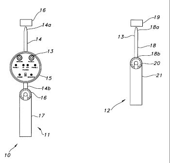
Referring now to Figure l, a capacitive test point voltage and phasing
detector 10 is
shown in use in an environment which is shown schematically. The capacitive
test point voltage
and phasing detector 10 generally includes a first detector member 1 l and a
second detector
member 12 which are in electrical communication with each other by a phase 2
lead 13, which is
merely a wire. Preferably the first detector member 11 includes a
longitudinally extended first
probe 14 having a pointed upper end 14a and a lower end 14b. The first
detector member 11 also
includes a circular shaped module 15 connected between the upper and the lower
end of the first
probe 14. The first probe 14 is configured to engage with a first capacitive
point 16 at the pointed
upper end 14a to take a voltage reading. The first probe 14 is electrically
coupled to the module
15. Moreover, a first universal adapter 16 is connected to the lower end of
the first probe 14 to
facilitate the attachment of the first detector member 11 to the non-
conductive stick 17 for use by
a technician in the field.
Similarly, the second detector member 12 also includes a longitudinally
extended second
probe 18 having a pointed upper end 18a and a lower end 18b. The second probe
18 is
configured to engage with a second capacitive point 19 at the pointed upper
end 18a to take a
voltage reading. The second probe 18 is electrically coupled to the module 15
through the phase
2 lead 13. Moreover, a second universal adapter 20 is connected to the lower
end of the second
probe 18 to facilitate the attachment of the second detector member 12 to the
non-conductive
stick 21 for use by a technician in the field. Both the first and second
probes are made from an
electrically conductive material. Preferably the first and second probes are
made from
aluminum.
The first detector member of the capacitive test point voltage and phasing
detector of
Figure 1 is shown in further detail in Figure 2. The first detector member 1 I
includes a first
probe 14 and a first universal adapter I 6. The first detector member 1 I also
includes module 1 S,
which preferably includes a display 20 and is configured to measure the actual
phase angle
difference between the first and second capacitive test points for determining
the phase
relationship between the capacitive test points. The module 15 also includes a
ground jack 21 for
connecting a ground lead to the system ground. A phase 2 jack 22 is also
mounted on the
module 1 S for accommodating one end of the phase 2 lead wire I 3 in Figure 1.
The module I 5 is
configured to enclose a battery to power the detector and includes a switch 23
to physically turn
4
CA 02360031 2001-10-25
the power on or off of the detector. Preferably the display 20 includes a
plurality of light
emitting diodes D1 through D6 together with textual indica or icons for
providing the indication.
The power diode DS is a light emitting diode which provides an indication that
the detector is
turned on or off and blinks to indicate that the battery is getting low. The
module display 20 also
includes a sensitive indicator D6 on the module, which is a light emitting
diode, which provides
an indication that the detector is in sensitive mode. Moreover the phase 1
diode D 1 on the
display indicates the presence of the voltage at the first capacitive test
point and the phase 2
diode D2 indicates the presence of the voltage at the second capacitive test
point. Finally the
module display includes an indication of whether the voltages are in or out of
phase on the
module display through diodes D4 and D3 respectively, thereby representing the
phase angle
relationship between the voltage at the first capacitive test point and the
voltage at the second
capacitive test point.
The operation of the detector 10 will now be explained with reference to both
Figures 1
and 2. Initially the detector 10 is turned on with the switch 23 and LED DS
will light to
acknowledge that the detector 10 is on. After the detector 10 is turned on,
each technician will
engage a probe with a capacitive test point. If both capacitive test points
are energized, both the
PHASE1 and PHASE 2 LED's, D1 and D2 respectively will light and the display
will provide
and indication whether the voltages are in or out of phase. If the voltages
are in phase, LED D4
will be lit preferably a green light. However, if the voltages are out of
phase, LED D3 will be lit
preferably a red light. If either or both capacitive test points are not
energized, no indication as
to whether the voltages are in or out of phase will be provided. That is, both
LED's D3 and D4
will not be lit. In addition, the technician will be able to identify which
capacitive test point or
points are not energized because the corresponding LED's D 1 and D2 will not
be lit. For
example, if the first capacitive test point 16 was not energized and the
second capacitive test
point 19 is energized LED's Dl, D4, and D3 will not be lit, but LED D2 will be
lit.
Referring now to Figure 3 the second detector member 12 of the capacitive test
point
voltage and phasing detector is shown in further detail. Besides including the
second probe 18
and the second universal adapter 20, it also includes a second probe jack 30
for accommodating
the other end of the phase 2 lead wire 13 in Figure 1.
CA 02360031 2001-10-25
Figure 4 shows in detail the switch 23 of the module display. The switch 23
includes
three positions from which a technician can select. The middle position 41,
which is the "ofi?'
position, indicates that the capacitive test point voltage and phasing
detector is turned off. The
upward position 42, the "on" position indicating that the detector is turned
on and is in normal
mode. The down position, 43 is called the sensitive position which also
indicates that the power
to the detector is turned on and is in a sensitive mode, and has some special
features which will
be explained hereto. In general, the capacitive test point systems operate in
the range of 1 S kV
(kilovolts) to 35 kV (kilovolts). It is known in the past that when a
technician uses the detector in
the "on" position 42, there will be a false indication of no voltage present
at the capacitive test
points if the system voltage is below 15KV(kilovolts). The diodes Dl and D2 in
Figure 2 will not
lite up even though there is voltage present at the two capacitive test
points. This is due to the
fact that the voltage is below the threshold of the detector. Therefore, under
this scenaxio, the
technician can switch to the sensitive position, 43 of the switch 23. When the
switch is in
sensitive position, 43, diodes D 1 and D2 will light up, giving an accurate
indication that there is
a presence of voltage at both capacitive test points. Also, sometimes due to
contamination at the
capacitive test point insulation surface and/or defects in the test point
system itself can give a
false representation of no voltage present at the capacitive test points to
the technician when the
switch 23 is at "on" position, 42. Again, by switching to the sensitive
position 43, under these
conditions, the technician will be provided with an accurate reading of the
presence of voltage at
the capacitive test points. The sensitive mode negates the factors such as
contamination in the
capacitive test points, the defects in the test point system itself and the
fact that the test point
systems is operating at a low voltage, and therefore, gives an accurate
indication of presence of
voltage independent of these factors.
The first detector member of Figure 2 includes a block diagram shown in Figure
5
illustrating phase detector circuitry. The input 51 of Figure 5 is the voltage
reading that is being
taken at the first capacitive test point 16 through the first probe 14 of
Figure 1 and the input 52 of
Figure 5 is the voltage reading being taken at the second capacitive test
point 19 through the
second probe 18 of Figure 1. The voltage readings are waveforms indicating the
presence of
voltage at the two capacitive test points. The voltage waveforms are
sinusoidal waveforms as
shown in Figures 6A and 6C as phase 1 and phase 2 representing the inputs 51
and 52
respectively of Figure 5. The voltage waveform at input 51 is the input to
operational amplifier
6
CA 02360031 2001-10-25
53 and voltage waveform at input 52 is the input to operation amplifier 54.
The operational
amplifiers 53 and 54 of Figure 5 are connected to ground through resistors 55
and 56
respectively. Resistors 55 and 56 are generally in the magnitude of tens of
kohms, preferably 22
kohms. Because the resistors 55 and 56 are at much lower values, the input
impedance in the
operational amplifiers 53 and 54 is very low. The low input impedance can
reliably determine
that the capacitive test point is energized even when the test point is
severely degraded,
providing signal data that can be used to reliably determine of the phase
relationship between
two capacitive test points. Also, the low input impedance is much less
susceptible to noise.
The operational amplifier 53 receives as input 51, the sinusoidal waveforms
phase 1 of
Figure 6A and Figure 6C, and the operational amplifier 54 receives as input 52
the sinusoidal
waveforms phase 2 of Figure 6A and Figure 6C. The output 57 of the amplifier
53 are square
waveforms phase 1 of Figure 6B and Figure 6D. The output 58 of the amplifier
54 are square
waveforms phase 2 of Figure 6B and Figure 6D.
The block diagram of Figure 5 also includes a power on self tester 59, which
is also an
input to the operational amplifiers 53 and 54. The power on self tester 59
provides an indication
that the detector is functioning properly by applying test waveforms to the
phase 1 input 51 and
the phase 2 input 52 of figure 5. The test waveforms apply an in phase
condition for
approximately 2 seconds and then an out of phase condition for an additional 2
seconds causing
diodes D1 through D4 of figure 2 to illuminate accordingly.
The output waveforms 57 and 58 if Figure 5 are input to the phase detector 60
which
determines the phase angle relationship between the voltage at the first
capacitive test point and
the voltage at the second capacitive test point. In particular, the phase
detector preferably
determines whether the voltages are in or out of phase and provides an
indication of same on the
display through LED's D4 and D3 as shown in Figure 2. As shown in Figure 6B,
as the square
waves in phase 1 and phase 2 go high or low at the same time indicates the
voltages at both the
capacitive test points are in phase. In Figure 6D, however, the square waves
of phase 1 and
phase 2 go high or low at different times, indicating a phase shift, i.e. the
voltages are out of
phase with respect to each other.
7
CA 02360031 2001-10-25
Preferably the block diagram of Figure 5 also includes a state detector
6lcoupled to
receiving the output waveforms 57 and 58. The switch 62, similar to the switch
in Figure 3 and
having normal and sensitive mode, is connected to the state detector 61. The
state detector 61
ensures that both the first capacitive test points and second capacitive test
points are energized
for protecting against the possibility of errors occurring when one or both
points are not
energized. The state detector 61 prevents the phase detector 60 from providing
an indication that
the voltages are in or out of phase unless both capacitive test points are
energized. This prevents
technicians from reaching a wrong conclusion when one or both capacitive test
points are not
energized. If both test points were not energized and the circuit did not
include a state detector
61, the phase detector 60 would determine that the voltages at the first and
second capacitive test
points were in phase. In other words, the state detector 61 is configured to
provide an indication
when voltage is present at a capacitive test point.
While the invention has been described by the foregoing detailed description
in relation
to the preferred embodiments with several examples, it will be understood by
those skilled in the
art that various changes may be made to specific methods and circuitry as set
forth in the present
invention without deviating from the spirit and scope of the invention as
defined in the appended
claims.
8