Note: Descriptions are shown in the official language in which they were submitted.
CA 02360291 2001-10-30
-1-
METHOD AND PROGRAM PRODUCT FOR DESIGNING HIERARCHICAL
CIRCUIT FOR QUIESCENT CURRENT TESTING AND
CIRCUIT PRODUCED THEREBY
[ 0001 ] The present invention relates, in general to the design and testing
of
integrated circuits and, more specifically, to a method and a program product
for
designing circuits in a manner to facilitate quiescent current (IDDq) testing
of the
circuit and to a circuit designed according to the method.
BACKGROUND OF THE INVENTION
[ 0002 ] The complexity of semiconductor circuits often requires partitioning
the circuit design into several core modules or blocks, generally referred to
as design
hierarchy. The blocks can be verified and laid out independently from each
other.
This design approach has been used for a long time and has several benefits,
the
most significant of which are to accelerate the development of the design by
allowing
several designers to work in parallel and to reduce the difficulty for design
automation tools by avoiding the need to manipulate the description of the
entire
circuit at once.
[ 0003 ] It has been shown recently that scan test methods can be adapted to
a hierarchical design methodology by adding scannable memory elements around
the periphery of core modules or by modifying functional memory elements near
the
periphery of modules and providing an internal and external mode of operation
to
these memory elements (see, for example, "A structured and Scalable Mechanism
for Test Access to Embedded Reusable Cores", ITC '98. paper 12.1, Marinessen
et
al. and Applicants' co-pending United States Patent Application Serial
No. 09/626,877 filed on July 27, 2000 for "Hierarchical Design and Test Method
and
System, Program Product Embodying the Method and Integrated Circuit Produced
Thereby", both incorporated herein by reference.) In this divide-and-conquer
approach, scan tests of modules can be prepared in advance by the designer of
the
core module or block without any knowledge of the context within which it will
be
used.
[ 0004 ] The preparation of the scan tests involves at least the verification
of
design-for-test rules and calculation of test coverage. During the internal
scan test
of blocks, the state of memory elements outside of the modules is irrelevant.
The
preparation also involves the generation of a simplified model of the module
that can
CA 02360291 2001-10-30
-2-
be used to perform the same steps at the next level of hierarchy of the
design. The
use of the simplified model eliminates the need to manipulate the entire
description
of core modules. During the external scan test of modules, the state of memory
elements that are not involved (i.e. not near the periphery of the module) is,
again,
irrelevant. Core modules can be tested in parallel or sequentially.
0005 ] There is one type of test that does not readily lend itself to this
hierarchical design methodology. During circuit manufacturing, it is often
required to
measure the quiescent current (IDDq) for different states of the circuit. The
quiescent current is used as a complement to the scan tests described earlier.
The
state of the circuit is defined by the values loaded in the memory elements of
the
circuit. The designer needs to ensure that each state of the circuit
corresponds to a
state where no static current is consumed in a good circuit. A software tool
(rules
checker) is typically used to perform this task. The designer can also
calculate the
fault coverage of the faults covered by this test using a fault simulator
and/or an
automatic test pattern generator (ATPG). To date, the quiescent current test,
and
the analysis required to perform it, requires considering the entire circuit
at once
which is becoming virtually impractical for large circuits.
SUMMARY OF THE INVENTION
[ 0006 ] The present invention provides a hierarchical design method for
integrated circuits to be tested using quiescent current monitoring and a
circuit
designed according to the method. The method allows the state of the entire
circuit
to be set in a repeatable and predictable manner which avoids the need to
analyze
the entire circuit at once. The circuit is divided into hierarchical blocks or
modules
according to a design hierarchy. The blocks have scannable memory elements
which are organized into scan chain segments with at least one segment being a
peripheral scan chain segment. The peripheral segment is comprised of input
and
output peripheral scannable memory elements which are configurable in an
internal
test mode and an external test mode.
[ 0007 ] One aspect of the present invention is broadly defined as a method of
designing integrated circuits, having at least one hierarchical block, for
quiescent
current testing, comprising analyzing each of one or more selected
hierarchical
blocks independently of other selected blocks in the same or higher levels of
hierarchy to identify circuit states of each the selected blocks which could
result in
elevated quiescent current levels during quiescent current testing of the
circuit, the
CA 02360291 2001-10-30
-3-
analyzing beginning with blocks at a lowest level of design hierarchy and
proceeding
in sequence through each level of design hierarchy to a highest level of
hierarchy
containing a top-level block; and calculating a fault coverage of for each the
selected
block.
[ 0008 ] Another aspect of the present invention is generally defined as a
circuit having at least one hierarchical block, the circuit comprising: each
block
having scannable memory elements arranged into two or more scan chain segments
having a serial input and a serial output, the memory elements including
peripheral
memory elements associated with block inputs and outputs, the peripheral
scannable
memory elements being arranged in peripheral scan chain segments, input
peripheral elements being configurable in internal test mode for testing
circuitry
within the block and output peripheral memory elements being configurable in
external test mode for testing circuitry external of the block; means
associated with
each segment and responsive to an active quiescent current test signal for
connecting the serial input of the segment to a block serial input, or to the
serial
output of another scan chain segment, or to the serial output of a peripheral
scan
chain segment of a block located at one level of hierarchy down; and means
responsive to the active quiescent current test signal for concurrently
configuring
input peripheral memory elements of the block in internal test mode and
configuring
output peripheral memory elements of the block in an external test mode during
quiescent current testing of the circuit.
0009 ] The layout of the circuit does not need to be hierarchical in order to
apply the proposed hierarchical quiescent current test method of the present
invention. However, if the layout of the circuit is hierarchical, the design
hierarchy
used for the layout will typically correspond to the top levels of the design
hierarchy
used for the test method.
[ 0010 ] Still another aspect of the present invention is defined asa method
of
performing quiescent current testing on an integrated circuit having at least
one
hierarchical logic block, each block having a block serial input, scannable
memory
elements arranged in at least one scan chain having a scan chain serial input,
the
method comprising connecting each block serial input to a circuit serial input
and
connecting each scan chain serial input to its associated block serial input;
serially
loading a quiescent current test pattern through the circuit serial input so
as to load
the test pattern into each scan chain in parallel until a predetermined
reference point
of the test pattern has been reached at which all scannable memory elements in
the
CA 02360291 2001-10-30
-4-
circuit have been initialized with a known value, and then performing a
predetermined number of quiescent current measurement steps including:
measuring the quiescent current of the circuit, storing the measured quiescent
current value and the test pattern point at which the value was measured; and,
while
the predetermined number of measurements has not been reached, scanning in an
additional sequence of bits of the test pattern and repeating the measurement
steps.
BRIEF DESCRIPTION OF THE DRAWINGS
[ 0011 ] These and other features of the invention will become more apparent
from the following description in which reference is made to the appended
drawings
in which:
[ 0012 ] FIG. 1 is a diagrammatic block view of a circuit according to one
embodiment of the present invention;
[ 0013 ] FIG. 2 is a diagrammatic view of a hierarchical block showing
scannable memory elements arranged in scan chains and peripheral memory
elements associated with block inputs and outputs;
[ 0014 ] FIG. 3 diagrammatically illustrates a prior art scannable memory
element;
0015 ] FIG. 4 diagrammatically illustrates a circuit having three levels of
hierarchy and showing the manner in which scan chain segments may be connected
according to one embodiment of the present invention;
0016 ] FIG. 5 is similar to FIG. 4, but shows a more restrictive manner in
which scan chain segments may be connected according to a preferred embodiment
of the present invention;
[ 0017 ] FIG. 6 is a flow chart illustrating the method of performing a
quiescent
current test on a circuit designed according to an embodiment of the method of
design of the present invention;
0018 ] FIG. 7 is a flow chart generally illustrating a method of designing a
hierarchical circuit for quiescent current testing according to an embodiment
of the
present invention;
0019 ] FIG. 8 is a diagram illustrating a single scan chain configuration for
two hierarchical blocks located one level down in design hierarchy from a
parent or
host block;
0020 ] FIG. 9 is a diagram similar to FIG. 8, but illustrating a parent block
scan chain configuration which includes all scannable memory elements of the
CA 02360291 2001-10-30
-5-
parent or top-level block and the peripheral memory elements of two
hierarchical
block located one level down in design hierarchy;
[ 0021 ] FIG. 10 is a diagram similar to FIG. 8, but illustrating a single
scan
chain configuration for each of a host block and two hierarchical blocks
located one
level down in design hierarchy, which is used when performing a quiescent
current
test of the circuit;
[ 0022 ~ FIG. 11 diagrammatically illustrates the alignment of the serial
input of
three scan chain segments receiving the same quiescent current test pattern
from a
pseudo-random pattern generator; and
[ 0023 ~ FIG. 12 is a state diagram of a Test Access Port according to the
IEEE 1149.1 standard.
DETAILED DESCRIPTION
[ 0024 ] In the following detailed description, numerous specific details are
set
forth in order to provide a thorough understanding of the present invention,
However, it will be understood by those skilled in the art that the present
invention
may be practiced without these specific details. In other instances, well
known
methods, procedures, components and circuits have not been described in detail
so
as not to obscure aspects of the present invention.
[ 0025 j As is known in the art, integrated circuit devices are typically
designed
and fabricated using one or more computer data files that define the layout of
the
circuit arrangements of the devices. The files are typically generated by a
design tool
and are subsequently used during manufacturing to create the layout masks that
define the circuit arrangements applied to a semiconductor wafer. Typically,
the
programs are provided in a predefined format using a hardware description
language
(HDL) such as VHDL, verilog, EDIF, etc. While the invention has and
hereinafter will
be described in the context of fully functioning integrated circuit devices
and data
processing systems utilizing such devices, those skilled in the art will
appreciate that
the various embodiments of the invention are capable of being distributed as a
program product in a variety of forms, and that the invention applies equally
regardless of the particular type of signal bearing media used to actually
carry out
the distribution. Examples of signal bearing media include but are not limited
to
recordable type media such as volatile and non-volatile memory devices, floppy
disks, hard disk drives, CD-ROM's, and DVD's, among others and transmission
type
media such as digital and analog communications links.
CA 02360291 2001-10-30
-6-
[ 0026 ] FIG. 1 illustrates a simple hierarchical circuit 10 according to one
embodiment of the present invention. The circuit includes a top-level
hierarchical
block 12, two embedded hierarchical functional blocks 14 and 16, a boundary
scan
register 18, a Test Access Port (TAP) 20, and a test controller 22. Reference
numeral 24 represents logic in top-level block 12. Blocks 14 and 16 are
contained
within or embedded in the top-level block and, thus, are located one level
down in
design hierarchy. Two hierarchical blocks are shown for illustration purposes
only. It
is to be understood that the circuit may have any arbitrary number of
hierarchical
blocks and levels. The TAP and boundary scan register are preferred, but not
essential to the invention. Typically. blocks 14 and 16 provide a unique
function.
There may be several reasons why these blocks are partitioned from the main or
host block, Some blocks may have been previously designed; others may have
been obtained from a third party core provider; still others may be formed by
encapsulating a large sub-circuit to simplify the design of the circuit.
[ 0027 ] FIG. 2 is a diagrammatic view of the internal structure of a typical
hierarchical block. The block generally includes combinational logic 30 and
block
inputs 32 and block outputs 34, by which the block communicates with other
blocks
during normal operation of the circuit, and memory or storage elements 36
which
store data during normal operation of the circuit as well as during various
test modes
of operation. The memory elements are designed to be scannable to allow a test
stimulus to be scanned into the elements and a test response data to be
scanned
out. FIG. 3 illustrates one arrangement of a typical scannable memory element
36.
The element receives input from combinational logic 30. The memory element
includes a flip-flop 38 having a data input, D, a data output Q and a clock
input, CK.
Input D is connected to the output of a multiplexer 40. One input 42 of the
multiplexer is connected to a memory element serial input, SI. The other input
44 of
the multiplexer is connected to an output of combinational logic 30. A control
input 46 of the multiplexer receives a scan enable signal, SE, which operates
to
configure the memory element in scan or shift mode when SE is active (logic 1
) and
in capture or normal mode when SE is inactive (logic 0). Output Q also serves
as
the memory element Serial Output, SO.
[ 0028 ] Referring again to FIG. 2, when scan enable SE is active, the
scannable memory elements are serially interconnected into one or more scan
CA 02360291 2001-10-30
_7_
chains 48 by connecting the serial output SO of each memory element to the
serial
input SI of another memory element. The serial input of the first memory
element in
the chain is connected to a scan chain serial input. The serial output of the
last
memory element in a scan chain is connected to a scan chain serial output. A
scan
chain segment is comprised of one or more memory elements.
[ 0029 ] Memory elements located at the periphery or boundary of a logic
block are referred herein to as "peripheral memory elements", but also known
in the
art as "partitioning scan cells". Elements which output a signal from the
block, such
as memory elements 50, are output peripheral memory elements. Elements which
receive a signal applied to the block, such as memory elements 52, are input
peripheral memory elements. The preferred form of peripheral memory elements
are of the type disclosed and claimed in Applicant's above mentioned co-
pending
United States Application Patent Application Serial No. 09/626,877 which uses
functional memory elements to partition a block into an internal partition and
an
external partition and thereby provide module or block isolation. However, the
present invention can be employed in a circuit which uses conventional test
dedicated peripheral memory elements. Both forms of peripheral elements are
described and illustrated in the aforementioned application.
[ 0030 ] Output peripheral memory elements are configurable in "external test
mode" in which data contained in the memory element is applied to its
associated
block output node which, in turn, is connected to external circuitry. When the
element is not in external test mode, data generated by the block is passed
through
to the output node. This allows test data to be scanned in to the output
peripheral
memory elements to test the response of external circuitry to various values
of block
outputs. Similarly, input peripheral memory elements are configurable in
"internal
test mode" in which data contained in the peripheral memory element is passed
on
to the internal circuitry of the block. When the element is not in internal
test mode,
data applied to its associated block input node is applied to the internal
circuitry of
the block. This allows test data to be scanned in to the input peripheral
memory
elements to test the internal logic of the block.
[ 0031 ] The top-level block need not necessarily be provided with peripheral
memory elements. In this case, the boundary scan register chain can be used as
a
peripheral chain. However, this is not necessary because access to chip inputs
and
outputs is available. Peripheral memory elements may be included in the top-
level
CA 02360291 2001-10-30
. $ _
block if the complete circuit may itself constitute a block which is embedded
into
another circuit.
0032 ] Input and output peripheral memory elements are normally not active
concurrently. In the present invention, however, the test controller is
provided with
circuitry (not shown) which responds to an active quiescent current test
signal by
applying a signal to input and output peripheral memory elements which
concurrently
configures input peripheral memory elements in internal test mode and output
peripheral memory elements in external test mode. This configuration is
referred to
herein as a "peripheral memory element quiescent current test mode". This mode
allows the peripheral memory elements to be arranged in a scan chain segment
and
a simplified model of embedded blocks to be substituted for the complete
description
of the block during analysis of a parent block, as explained more fully later
in the
description of the method of the present invention. In addition, it allows
test data
scan in to input and output peripheral memory elements to be concurrently
applied to
block internal logic as well as to logic external to a block.
( 0033 ) One aspect of the present invention relates to the manner in which
internal and peripheral memory elements are arranged into scan chains for use
in
loading quiescent current test patterns into the various hierarchical blocks
in the
circuit. In general, memory element segments of a block are arranged, in IDDq
test
mode, on a scan path which originates from or includes a block serial input.
This is
achieved by connecting segment serial input to: A) a block input, B) the
serial output
of another segment or C) the serial output of a segment located in an embedded
block one level down in design hierarchy and by connecting the block serial
input of
embedded blocks to the block serial input A segment comprises one or more
serially configurable scannable memory elements.
0034 ] This configuration allows the use of a simplified or shell model of a
block during a block analysis design phase, described later. The simplified
model
contains peripheral memory element segments and peripheral logic and
additional
files which describe the scan paths of the block and the scan paths of
embedded
blocks and allows for pattern generation. In this arrangement, some rules
checking
(e.g. scan path continuity) and verification/simulation is performed in an
indirect
manner in which other scan test modes are rules checked and verified/simulated
and
it assumed that the IDDq test mode is correct by construction. Thus, this
general
configuration does not place any restrictions on internal and peripheral
segments.
CA 02360291 2001-10-30
_g_
[ 0035 ] This configuration also allows the use of simplified models which
contain all scan paths and peripheral logic which, in turn, allows for a
complete
analysis including rules checking, pattern generation and verification (i.e.
simulation).
The configuration provides significant size reduction in the size of
simplified models,
but is not optimal.
[ 0036 ] This general configuration will be better understood by referring to
FIG. 4 which illustrates a circuit having three levels of hierarchy. The
figure shows
three blocks including a top level block 60 having an embedded block 62 which
defines a second level of hierarchy and which, in turn, has an embedded block
64
which defines a third level of hierarchy. Scan chain segments are shown as a
sequence of rectangles which represent memory elements. Peripheral segments
are bolded. A segment may consist of one or more scannable memory elements.
Blocks 60, 62 and 64 are provided with block serial inputs 66, 68 and 70,
respectively. For simplicity, each block is shown as having only one block
serial
input. However, more than one block serial input may be provided without
departing
from the spirit of the invention. Host block 60 includes two internal segments
72 and
74 and no peripheral segments. Segment 72 is connected to top level block
serial
input 66, the chip circuit input. Embedded block 62 includes two internal
segments 76 and 80 and a peripheral segment 78. In this simple example, block
62
is provided with means, in the form of a multiplexer 82, for selectively
connecting the
serial input of peripheral segment 78 to one of two sources including the
output of
internal segment 76 of block 62 or to the serial output of internal segment 72
of
parent block 60. Multiplexer 82 is controlled by a control signal C1. The
output of
peripheral segment 78 is connected to the input of internal segment 74 of
parent
block 60.
[ 0037 ] Embedded block 64, which resides in the third level of hierarchy, has
four segments, including internal segments 84, 86 and 88, and peripheral
segment 90. Segments 84 and 86 are serially connected together, with the input
of
segment 84 being connected to block serial input 70. A multiplexer 92 receives
the
serial output of peripheral segment 78 in parent block 62 and the output of
internal
segment 86 and applies its output to peripheral segment 90. Multiplexer 92 is
controlled by control signal C2. The serial output of peripheral segment 90
branches
to internal segment 80 of parent block 62 and internal segment 88 of current
block 64. It will be seen that all segments reside on scan path which
originates from
CA 02360291 2001-10-30
-10-
or includes a block serial input. The serial input of block 64 is connected to
the serial
input of parent block 62. Control signals C1 and C2 are mode signals which are
used to define different scan chains configurations for scan testing and
quiescent
current testing of the circuit. A specific example of various modes is given
below
with reference to FIG. 5.
[ 0038 ] It will be seen that the general configuration described above allows
segments which depend on internal segments of embedded blocks. In some cases,
this can lead to complications with regard to generating and verifying test
patterns to
be used during quiescent current testing. The situation can be simplified by
placing
restrictions on the connections of internal and peripheral scan chain segments
as
described below.
[ 0039 ] In IDDq test mode, internal segments are arranged on a scan path
which originates from or includes a block serial input by connecting the
internal chain
segment serial input to: A) a block input, B) the serial output of another
segment
(internal or peripheral) in the block or C) the serial output of a peripheral
segment
located in an embedded block one level down in design hierarchy. Thus, the
primary
difference between this configuration and the general configuration described
above
is with regard to the option (C). More specifically, if an internal segment is
connected to any segment in an embedded block, it must be connected to the
output
of a peripheral segment.
[ 0040 ] In IDDq test mode, peripheral segments are arranged on a scan path
which originates from or includes a block serial input by connecting the
peripheral
segment serial input to: A) a block input, B) the serial output of another
peripheral
segment of the block or C) the serial output of a peripheral segment located
in an
embedded block. Thus, this limits the sources for peripheral segments to
either the
block serial input or to the output of another peripheral segment in its
resident block
or in an embedded block. This configuration is illustrated in FIG. 5 which has
the
same three blocks and scan chain segments as in FIG. 4 and uses the same
reference numerals used in the latter to designate like parts. Referring to
FIG. 5, it
will be seen that internal segments 74 and 80 have their serial inputs
connected to
the output of segments in an embedded block. In both cases, the source is the
output of a peripheral segment, namely segments 76 and 90, respectively. All
other
internal blocks are connected to other segments in their respective block. The
circuit
is in IDDq mode when control signals C1 and C2 are both active (logic 1). The
scan
chains which are formed in this mode are indicated by the solid lines which
CA 02360291 2001-10-30
-11-
interconnect the various segments. The dotted lines indicate other scan test
modes.
Thus, it will be seen that, in IDDq mode for the FIG. 5 example, peripheral
segments 76 and 90 are connected directly to their respective block serial
input and
are the first segment in their respective scan chains. In IDDq mode, the
circuit of
FIG. 5 has four chain chains which together collect all memory elements in the
circuit. A first scan path comprises segment 72 in block 60; a second scan
path
comprises segments 76, 78, and 74; a third scan path comprises segments 84,
86,
90 and 80; and a fourth scan path comprises segments 90, 84, 86 and 88.
[ 0041 ] In addition to defining an IDDq mode, control signal C1 and C2,
define
three scan test modes which are used to test the three blocks individually. C1
and
C2 are set to 0,0 to perform a scan test of top level block 60. The scan path
formed
collects segments 72, 78 and 74. C1 and C2 are set to 0,0 to perform a scan
test of
block 52. The scan path formed collects segments 76, 78, 90 and 80. C1 and C2
are set to [0,1 ] to perform a scan test of embedded block 64. The scan path
formed
collects segments 84, 86, 90 and 88. It will be noted that the scan chains for
blocks 60 and 62 include the peripheral segment of their embedded blocks. It
will be
understood by those skilled in the art that other scan chains may be formed
for other
tests.
[ 0042 ] The specific inter-block connections shown in FIG. 4 and 5 are for
illustration purposes to show some possible connections. In the preferred form
of
the invention, each block, including the top level block, is provided with a
single scan
chain configuration which collects all scannable memory elements which reside
in its
block and the serial input of each scan chain is connected to the circuit
serial input,
the Test Data Input (TDI) of the TAP. This is illustrated in FIG. 11. This
scan chain
includes both internal and peripheral memory elements. All of the scan chains
are
concurrently enabled in response to a quiescent current test mode signal so
that
quiescent current test patterns can be concurrently loaded into all blocks in
the
circuit. Preferably, the same test patterns are concurrently loaded into all
blocks
and the patterns are pseudo random patterns. However, some blocks may require
block specific patterns, as mentioned above. The serial input of such a block
is
connected to a separate source via a circuit primary input. The test patterns
from
the separate source are loaded into the block concurrently with the loading of
test
patterns into the other blocks.
CA 02360291 2001-10-30
-12-
0043 ] A circuit constructed as described above may have quiescent testing
performed as described below with reference to FIG. 6 which illustrates a flow
chart
of the various steps of the method. The circuit is placed in quiescent current
test
mode (step 100) by applying an appropriate instruction to the chip. In
response, the
test controller generates an appropriate Mode signal whereby the serial input
of each
block is connected to its predetermined circuit primary serial input, such as
the TDI
pin of the TAP, and the serial input of each block scan chain is connected to
the
block serial input. In the simplest form of the method, the serial input of
blocks
embedded in other blocks (i.e. blocks located at one level down in design
hierarchy),
are connected to the block serial input of their respective parent block. This
establishes a scan path to all scannable memory elements in all blocks in the
circuit
and, more specifically, a plurality of parallel scan paths.
[ 0044 ] Quiescent current test patterns are then serially loaded through the
circuit serial inputs) and into each scan chain in parallel until a
predetermined
reference point of the test pattern has been reached. This is achieved by
setting SE
high and activating the clock signal applied to the memory element clock
inputs
(step 102). The test patterns will include an initialization section which
serve to
initialize all memory elements to a known value (step 104). When the sequence
of
bits of the test pattern reaches a certain predetermined point, referred to
herein as a
"reference point", quiescent current measurement procedures, indicated
generally by
reference numeral 106, begins. Procedure 106 comprises performing a
predetermined number of quiescent current measurement steps. These steps
include measuring the quiescent current of the circuit (step 108), and storing
the
measured quiescent current value, and the test pattern point or number at
which the
value was measured (step 110). As long as the predetermined number of
measurements have not been made (step 112), an additional sequence of bits of
the
test pattern is loaded (step 114) and the current measurement and storage
steps
108, and 110, are repeated. When the predetermined number of measurements
have been made, the procedure is terminated (step 116) and the results are
analyzed using known methods to determine faults, if any, in the chip. In a
preferred
embodiment of the method, the test pattern is a pseudo-random sequence of
bits.
0045 ] The present invention also contemplates simultaneously loading
different sequences of bits, from different sources, into different blocks as
well as
blocks have more than one quiescent current serial input for loading different
sequences of bits into different scan chains of the same block.
CA 02360291 2001-10-30
-13-
[ 0046 ] As mentioned, during testing, a scan enable signal and a clock signal
are used to control scan path segments. The scan enable signal and clock
signal
can be applied directly to circuit inputs or to inputs of the TAP. When a TAP
is
provided and boundary scan is used in the top-level block, it might be
necessary to
scan predetermined values into the boundary scan register (step 119) prior to
performing the IDDq measurement steps, to place circuit inputs and outputs in
a
condition that will not cause an elevated quiescent current. Referring to FIG.
12,
which illustrates the various states of a TAP according to the IEEE 1149.1
standard,
the scan enable signal is active during the Shift_DR state of the TAP and
inactive
when the TAP is in another state. Clock pulses are generated only during the
Capture DR and Shift DR states of the TAP. The predetermined values are loaded
into the boundary scan register by transitioning the TAP through the Select
DR,
Capture, Shift, Exit1 and Update states. After shifting for an appropriate
number of
clock cycles, a measurement can be made while still in the shift cycle or,
alternatively, by transitioning the TAP to the Exit1, Pause or Exit2 states.
Going for
the Pause or Exit states cause the scan enable (SE) signal to go low. This has
the
merit of testing the memory elements in their functional mode of operation.
After a
measurement has been made, step 114 (load more bits) is performed by
transitioning back to the Shift state without traversing the Update state.
This
preserves the predetermined values loaded in step 119. In this way, once a
test
pattern has been shifted in, the current measurements are taken for various
combinations of the scan enable and clock signals to maximize the fault
coverage.
This can also be achieved in a circuit which does not have a TAP.
[ 0047 ] The description now turns to the method of designing blocks to enable
a circuit for quiescent current testing according to the present invention. As
is
evident from the foregoing, the quiescent current test method of the present
invention employs a scan mode of operation by which quiescent current test
patterns
are shifted into memory elements of the entire circuit. The method is such
that it is
not only repeatable, but also predictable. The operations described below are
performed on a description of a circuit under development.
[ 0048 ] It is assumed at the outset that functional memory elements in all
blocks have been converted to scannable memory elements to include a
multiplexer,
such as multiplexer 40 in FIG. 3 so that the memory elements are configurable
in
scan mode and capture mode, and provision has been made to provide peripheral
CA 02360291 2001-10-30
-14-
memory elements. Test dedicated memory elements may be inserted between the
output of combinational logic of the block and the output node of the block.
Alternatively, as described and claimed in Applicant's co-pending application,
supra,
functional memory elements at the periphery or boundary of each block are
converted to peripheral memory elements. In the illustrated examples of FIG.
1, 4
and 5, each of the blocks shown therein have been so modified.
[ 0049 ] The following steps are performed on selected blocks in the circuit.
It
will be understood by those skilled in the art that any sub-circuit may be
selected or
designated as a hierarchical block. Each selected block is provided with
peripheral
memory elements.
[ 0050 ] The first step is to arrange the internal scannable memory elements
in
each hierarchical block into scan chains according to the rules described
earlier with
reference to FIG. 4 and 5 and to insert means in the circuit for concurrently
configuring input peripheral memory elements in internal test mode and output
peripheral memory elements in external test mode. These configurations are
based
on the principle that the test patterns generated for each block will be
applied to the
serial input of the block and that the block serial input is ultimately
connected to a
circuit serial input. This arrangement is necessary to determine a "reference
point"
of a predetermined sequence of bits applied to the serial inputs) when
performing
quiescent current measurements, as explained more fully later. This step is
performed by an appropriate software tool which determines the appropriate
scan
chains from the circuit description using the above described segment
connection
rules.
[ 0051 ] Once the scan chain segments and chains in a hierarchical block
have been defined and the block descriptions modified, each selected block is
analyzed to determine whether there exist any circuit states which would cause
an
elevated quiescent current. As shown in the flow chart of FIG. 7, the analysis
is
performed on individual blocks in isolation. The analysis begins with the
blocks at
the lowest level of hierarchy and progresses upwardly to the highest level.
This is
referred to as a bottoms-up analysis. The circuit in FIG. 4 and 5 will be used
as an
example. Thus, the lowest level is selected first (step 120) and then a block
is
selected (step 122) in the selected level. In the example, the lowest level is
level
three which has one block, block 64. Block 64 is selected . The block is then
analyzed (step 124) to determine whether it contains circuit states which
would result
in elevated IDDq current levels. This is followed by the generation of test
patterns
CA 02360291 2001-10-30
-15-
(step 126) and the calculation of fault coverage (step 128) which is stored.
Finally,
the test patterns are simulated or verified (step 130). The patterns are fault
simulated using any desired fault model such as a "toggle fault model" or a
"pseudo
stuck-at fault model", both of which are well known to those skilled in the
art. If there
are more blocks in the hierarchical level (step 132), the next block is
selected
(step 134) and steps 124 to 130 are repeated. In the illustrated example,
there are
no other blocks in the third level. If all blocks in the current level have
been
processed and there are more levels to analyze (step 136), the next level is
selected
(step 138) and steps 122 to 136 are repeated. In the example, the second level
is
processed and block 62 is selected for analysis. Once block 62 has been
analyzed,
the top level is processed and top level block is selected for analysis. When
all
levels have been processed, the procedure is complete. The above steps will
now
be described in more detail.
[ 0052 ] When analyzing the circuit description (typically, a gate level
description) of an individual block during the design process, quiescent
current test
patterns are generated and applied to the logic within the block and to the
logic at
the next level down of design hierarchy via the peripheral memory elements of
the
blocks selected for analysis. Embedded blocks located one level down in design
hierarchy, if any, are configured in peripheral memory element quiescent
current test
mode.
0053 ] Preferably, a simplified or shell model of selected embedded
hierarchical blocks is generated for use during analysis of its parent block.
The
simplified model is substituted for the complete description of the embedded
block.
This substitution simplifies the analysis. Simplified models need not be
generated
for all embedded blocks, but rather may be limited to certain blocks, such as
blocks
which exceed a predetermined size. The simplified model may contain only the
peripheral scannable memory elements or, additionally, some peripheral logic,
as
described and claimed in Applicant's aforementioned application No.
09/626,877.
Further particulars of the analysis procedure are described below in the
description
of variations of the method which are used for different types of blocks. The
analysis
is performed using the same test patterns which will be used during actual
testing of
the circuit and will identify test patterns which must be excluded.
0054 ] For a block which contains embedded blocks, the fault coverage of
the block is first calculated by considering only the logic contained within
the block
itself and the peripheral logic of embedded blocks located at one level down
in the
CA 02360291 2001-10-30
-16-
design hierarchy. The total fault coverage of the block is calculated by
determining
the weighted sum of the fault coverage of the block and of its embedded
blocks.
The fault coverage block is weighted by the number of gates contained in each
block. It will be noted that the fault coverage of an embedded block can
itself be the
result of a weighted sum because of embedded blocks that are further down in
the
design hierarchy.
( 0055 ] The simulation or verification of the application of the test
patterns to
verify their correctness, is optional in a design environment in which the
connections
of the various scan segments are automated. However, it might be desirable to
perform such simulation in a circuit simulator (e.g. Verilog or VHDL) with
full timing
information to ensure that the circuit will operate as predicted.
( 0056 ] The steps of analysis, test pattern generation and fault simulation
are
performed on a circuit representation which includes only the boolean function
of
circuit gates. Timing considerations are not taken into account. The
simulation
consists of scanning in the test patterns and observing that the desired bit
values
have been loaded in the correct memory elements at the predicted time. The
simulation can be performed either by simulating the entire circuit, i.e. all
blocks,
simultaneously, or by simulating the host circuit and a simplified model of
each of its
embedded blocks. When a simplified model is used for embedded blocks, the most
efficient way of organizing the scan path segments inside the embedded blocks
is to
connect all peripheral scan path segments to a block input or to the output of
another
peripheral scan path segment so that all peripheral memory elements are at the
beginning of the scan path segments and the simulation results of a block do
not
depend on values shifted through internal scan path segments. Verification can
also
be performed in a fully hierarchical /manner.
( 0057 ] As mentioned above, certain steps of the methods of designing differ
slightly from one another, depending on the nature or type of block. The
following
description addresses these variations. There are two variations of the basic
method
that will be described. Both variations rely on the application of a standard
predetermined sequence of bits to the serial inputs of blocks. Preferably, all
blocks
have a single serial input so that all blocks can be connected to the same
test
pattern source. The first variation is based on the premise that test patterns
do not
need to be carefully chosen and that, in a good circuit, no circuit states
result in
elevated quiescent current. The second variation is based on the premise that
test
patterns do not need to be carefully chosen and that, in a good circuit, most
circuit
CA 02360291 2001-10-30
-17-
states will not result in elevated quiescent current. Thus, this variation
contemplates
that some states result in an elevated quiescent current and includes steps to
identify test patterns which create elevated quiescent current conditions.
First Variation
0058 ] As previously mentioned, the first variation is based on the premise
that test patterns do not need to be carefully chosen and that, in a good
circuit, no
circuit states will result in an elevated quiescent current. This variation
allows a
block provider to perform all steps necessary to prepare a block for quiescent
current
testing, according to the present invention, without having to provide
detailed
information about the internal structure of the block to the user of the
block.
0059 ] Both variations use predetermined sequences of bits that are not
block specific. The same sequence of bits is applied to the serial input of
all blocks
of these types. The sequence is preferably a pseudo-random sequence, but it
can
be any sequence as long as it is extendable, both forward and backward, from a
"reference point", so that all of the memory elements of the longest chain are
initialized. A pseudo-random sequence is preferred because of the ease with
which
it can be to generated algorithmically either on-chip or off-chip. Test
pattern
generation can be implemented by means of either hardware or software.
Predetermined sequences can also be stored in tester memory as well.
0060 ] The analysis phase determines whether certain circuit states result in
elevated quiescent current. In the first variation of the method, the result
of the
analysis must indicate that there are no such states. An indication that there
are
such states means that there is an error in the design of the block and the
error must
be rectified. The analysis can be a static analysis performed independently of
the
aforementioned predetermined sequence of bits which will applied to the serial
inputs
during quiescent current testing of the circuit. A static analysis assumes
that all
circuit states are possible. While the analysis is more complex than other
types of
analyses, it is exhaustive in that it can verify that any predetermined
sequence can
be applied to the circuit. The analysis may, alternatively, consist of a
simulation of
the logic contained in the block using the predetermined sequence of bits
applied to
the block serial input during actual quiescent current testing. While a
simulation
analysis is simpler than a static analysis, it is not exhaustive in that the
results
obtained with a specific sequence are not necessarily applicable to other
sequences.
CA 02360291 2001-10-30
-18-
0061 ] The quiescent current test pattern for the circuit is designed so that
it
includes an initialization section and a quiescent current measuring section.
The
initialization section serves to initialize all scannable memory elements in
the circuit
to a known value. A "reference point" in the predetermined sequence is the
point at
which quiescent current measuring begins. Assuming a single serial input for
each
block (the case of multiple serial inputs is discussed later) and a maximum
chain
length L, the L bits of the predetermined sequence preceding the reference
point
must be known as these bits will determine the contents of the scan chain.
[ 0062 j Starting from the reference point of the predetermined sequence, the
test patterns resulting from shifting the predetermined sequence are
calculated and
the fault coverage is calculated for each of a predetermined number of current
measuring points after the reference point of the predetermined sequence. The
measuring points are the same for all blocks and can be at regular intervals
of the
predetermined sequence. By aligning the reference point, i.e. by concurrently
loading the same test pattern into all quiescent current scan paths in all
blocks, it is
possible to perform the analysis of each block in isolation without knowing
anything
about the other blocks. The procedure to generate the test pattern for each
block is
performed in such a way that it will be possible to apply the patterns after
the block
has been inserted on a chip. The procedure is as follows. A Pseudo Random
Pattern Generator (PRPG) sequence (see FIG. 11) is applied with a constant,
predetermined polynomial and seed to all blocks. The PRPG seed corresponds to
the PRPG value at the time the first current measurement is performed.
Subsequent
current measurements are performed at predetermined intervals, such as every
100
clock cycles for as many current measurements as are desired. Depending on the
length of the scan chain of a given block, the PRPG is rolled back by N states
to
determine the starting seed value to load in the PRPG and begin generating the
sequence for the block. N corresponds to the length of the scan chain. This
approach of aligning the seed at the first measurement instead of at the
beginning of
the sequence allows aligning the sequence for multiple blocks which have
different
scan chain lengths. The longest sequence is chosen so that all blocks end up
in the
same predicted state at the time of the first (the reference point of the
sequence)
and the subsequent current measurements. Extra TDI values are simply flushed
out
at the other end for the smaller scan chains.
CA 02360291 2001-10-30
-19-
[ 0063 ] The first measurement corresponds to the reference point mentioned
previously. At the time of the first measurement, the first memory element of
all
chains contains a value corresponding to TDI timeslot 0. The next memory
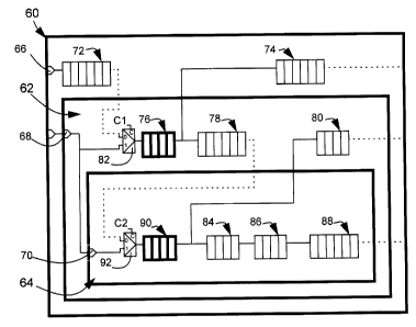
element
contains TDI timeslot -1 and so forth. The same predicted values apply to
subsequent measurements and is independent on the length of each scan chain.
[ 0064 ] When the various blocks are integrated into a circuit, the block with
the longest chain will determine the length of the initialization section,
i.e., the
number of bits which must be provided before the reference point to completely
initialize all chains. For example, assume that block 14 has a scan chain
length of
30,000 and block 16 has a chain length of 50,000. Block 14 is analyzed using
only
the 30,000 bits before the reference point to initialize all memory elements.
Block 16
is analyzed using the 50,000 bits before the reference point. When the circuit
is
actually tested, the 50,000 bits before the reference point are applied to the
circuit to
initialize the longest chain. However, the first 20,000 bits will be ignored
by block 14
as it only needs the last 30,000 bits. The last 30,000 bits will correspond
exactly to
those used to perform the analysis of block 14 in isolation and the 50,000
bits will
correspond exactly to those used to perform the analysis of block 16 in
isolation.
( 0065 ] From the reference point, current measurements are performed every
time a certain number of new bits of the sequence have been shifted in. This
number is arbitrary. However, a standard number can be used so that the fault
coverage can be computed in advance for all blocks. For example, a measurement
interval of every 100 bits of the predetermined sequence would be acceptable.
[ 0066 ] The analysis of the blocks is bottom-up. That is, the blocks at the
lowest level of the design hierarchy are analyzed first and the information
necessary
to analyze the block at the next higher level of hierarchy is generated and
stored.
The information would include, for example, the values output by the output
peripheral memory elements.
[ 0067 ] Generally, blocks will have only one block serial input. However,
more
than one block serial input may be provided if desired without departing from
the
invention. The advantage of using several serial inputs is that it might
reduce the
test time because it takes less time to load the scan paths. However, the
dominant
factor is usually the time required to perform the current measurement as
opposed to
the time required to load the patterns. Multiple serial inputs would only be
required
when the scan chain length of a block is very large (e.g. more than a million
memory
CA 02360291 2001-10-30
-20-
elements). Individual scan chains in the block would be connected to only one
of the
block serial inputs.
0068 ] The same predetermined sequence of bits can be applied to all inputs
or, alternatively, different sequences can be applied to different inputs. The
use of
different sequences for different serial inputs might provide a slightly
higher fault
coverage. The use of the same sequence for all serial inputs simplifies the
connections. This is because, if each serial input is associated with a
specific
predetermined sequence, the connections made at the next level of design
hierarchy
must take this association into account. The same predetermined sequences are
used for all embedded blocks. That is, serial inputs of different blocks can
be
connected together. In this variation, the analysis requires only one pass
through
the various blocks of the circuit.
[ 0069 ] FIGS. 8-10 illustrate scan chain configurations which are obtained in
accordance with the present invention. The three figures illustrate different
scan
chain configurations for the same circuit. Scan chain segments are indicated
by an
alphabetical character inside a circle. Segments positioned adjacent the
perimeter
of a block are peripheral memory elements. The arrows indicate scan path shift
direction. Each figure shows the circuit 10 as having a Test Data Input pin,
TDI,
which serves as the circuit as well as the block serial input for quiescent
current test
patterns.
[ 0070 ] Referring to FIG. 8, host block 12 comprises segments labeled A, B,
K, L, M, N, Q, V. Block 14 consists of segments C, D, E, F, G, H, I and J.
Block 16
comprises segments O, P, Q, R, S, T and U. A single scan chain configuration
is
shown for each block. The first segment of each single chain is connected to
the
TDI pin, which is the serial input of the host block. The single scan chain of
each
block collects all memory elements within its associated block, including both
the
internal and peripheral memory elements. The order of the memory elements in
each segment is extracted for each block separately and stored in a respective
block
scan chain file in memory.
[ 0071 ] FIG. 9 illustrates a single chain configuration which is used when a
host or parent block 12 is selected for analysis. The single scan chain of the
top
level block collects all top level memory elements and the peripheral memory
elements of collared or embedded hierarchical blocks 14 and 16.
0072 ] FIG. 10 illustrates the scan configuration that is obtained when both
embedded blocks 14 and 16 and the top level block 12 are placed into their
CA 02360291 2001-10-30
-21 -
respective single chain configuration. It will be seen that, in this
configuration, all
memory elements in all blocks have been collected. This is the scan chain
configuration which is used when a quiescent current testing is performed on a
physical chip and when the entire chip is analyzed at once. It will be noted
that
certain peripheral memory elements within hierarchical blocks 14 and 16, drive
two
destinations. For example, memory element U drives memory elements S and V.
This type of scan chain branching is normally not allowed in scan based tests,
but
does not create any problems in quiescent current testing because the scan
chains
are only used to control the states of the memory elements, but not to observe
them.
Observation in a quiescent current test is achieved by current measurements,
not by
comparing the scanned out values of the memory elements. The other point to
note
is that the value of V depends on the value of internal segment R. The only
information required about this segment is its length. This information is
extracted
during the analysis of embedded block 16 and can be made easily available
during
the analysis of parent block 12.
0073 ) As with a normal scan chain, the position of each memory element in
the scan chain is associated to a "timeslot" on TDI except that, due to the
branching
effect, more than one memory element can be associated with any given
timeslot.
The consequence of the branching is that values within memory elements are
forced
to be the same for all memory elements associated with a unique timeslot on
TDI.
This avoids loading of independent values in each hierarchical block. The
random
vector method described herein exploits this feature and allows for fault
grading each
block independently of all other blocks while obtaining a consolidated fault
coverage
of the entire chip without ever having to load the entire netlist into any
analysis tool.
[ 0074 ] When performing the analysis of this circuit, blocks 14 and 16 are
analyzed before host block is analyzed. Being in the same hierarchical level,
the
order in which blocks 14 and 16 are analyzed is not important.
Second Variation
[ 0075 ) The second variation is based on the premise that test patterns do
not
need to be carefully chosen and that, in a good circuit, most, but not all,
circuit states
will not result in elevated quiescent current. Thus, this variation assumes
that there
may be some states which result in an elevated quiescent current. In contrast
with
the first variation, the second variation is most useful when the circuit
designer has
access to detailed information respecting all hierarchical blocks because a
fault
CA 02360291 2001-10-30
-22-
simulation must be performed on the hierarchical blocks after the blocks have
been
assembled on the circuit. The method identifies test patterns which result in
elevated quiescent current states and excludes them from use during analysis
and
quiescent current testing of the circuit.
[ 0076 ] In this variation, analysis of the circuit is performed in two
passes.
Each pass are performed bottom-up, i.e. from the lowest level of design
hierarchy to
the highest level. The first pass identifies the points of the sequence where
current
measurements can be performed. The second pass calculates fault coverage based
on the portion of the sequence that were actually used.
[ 0077 ] During the first pass, starting with the blocks at the lowest level
of
design hierarchy, each block is analyzed and a set of constraints is appended
to
information passed to the next level of design hierarchy. The constraints
identify the
points of the sequence which correspond to elevated quiescent current and also
specify test pattern information. The constraint information can be appended
to a
log file produced by an analysis tool. The analysis at the next higher level
considers
the constraints of all embedded blocks and excludes all points of the sequence
where at least one block indicated that it corresponded to an elevated
quiescent
current. This new set of constraints is stored for use in the analysis in the
next
higher level of design hierarchy where additional points may be excluded based
on
the analysis at that level. Once the top and final level block has been
analyzed, all
usable, or non-usable, points of the sequence have been identified.
[ 0078 ] During the second pass, test patterns corresponding to the usable
points of the sequence are fault simulated and the fault coverage is
calculated.
Again, the blocks at the lowest level of hierarchy are analyzed first and the
fault
coverage results are stored for use in the next higher level of design
hierarchy along
with the number of gates in the block so that the total fault coverage of the
next
higher level can be calculated.
[ 0079 ] All the connections indicated in the description in the claims are
"logical" connections meaning that the connections are made during the test
mode of
interest (i.e. quiescent current measurements). This means that the
connections
could be made through logic (e.g. multiplexers or other gates) as opposed to
direct
connections.
[ 0080 ] Although the present invention has been described in detail with
regard to preferred embodiments and drawings of the invention, it will be
apparent to
CA 02360291 2001-10-30
-23-
those skilled in the art that various adaptions, modifications and alterations
may be
accomplished without departing from the spirit and scope of the present
invention.
Accordingly, it is to be understood that the accompanying drawings as set
forth
herein above are not intended to limit the breadth of the present invention,
which
should be inferred only from the following claims and their appropriately
construed
legal equivalents.