Note: Descriptions are shown in the official language in which they were submitted.
CA 02360323 2001-07-11
WO 00/55908 PCT/US99/28442 r
LAMINATE FOR MULTI-LAYER PRINTED CIRCUIT
Field of the Invention
The present invention relates generally to printed circuits, and more
specifically, to components employed in the manufacturing of printed circuit
boards.
Background of the Invention
In recent years, printed circuit components have become widely used in a
variety of electronic devices. Of particular interest are mufti-layer printed
circuit
board laminates which have been developed to meet the demand for
miniaturization of
electronic components and the need for printed circuit boards having a high
density of
electrical interconnections and circuitry. In the manufacture of printed
circuit boards,
raw materials, including conductive foils, which are usually copper foils, are
secured
to opposite sides of a core which is conventionally a reinforced or non-
reinforced
dielectric. (Throughout this specification, the use of the term "core" is
meant to
include any one of a variety of core materials, all of which may be reinforced
or non-
reinforced and may include an epoxy, polyester, polyimide, a
polytetrafloroethylene,
and in some applications, a core material which includes previously formed
printed
circuits.)
The process includes one or more etching steps in which the undesired or
unwanted copper is removed by etching away portions of the conductive foil
from the
laminate surface to leave a distinct pattern of conductive lines and formed
elements on
the surface of the etched laminate. The etched laminate and other laminate
materials
may then be packaged together to form a mufti-layer circuit board package.
Additional processing, such as hole drilling and component attaching, will
eventually
complete the printed circuit board product.
The trend in recent years has been to reduce the size of electronic components
and provide printed circuit boards having mufti-chip modules, etc. This
results in a
need to increase the number of components, such as surface-mount components
provided on the printed circuit board. This in turn results in a so-called
"densely
populated" or simply "dense" printed circuit board. A key to providing a
densely
populated printed circuit board is to produce close and fine circuit patterns
on the
outer surfaces (i.e., the exposed surfaces) of the resulting mufti-layer
printed circuit
board. The width and spacing of conductive paths on a printed circuit board
are
CA 02360323 2001-07-11
WO 00/55908 PCT/US99/28442
2
generally dictated by the thickness of the copper foil used thereon. For
example, if the
copper foil has a thickness of 35 pm (which is a conventional 1-ounce foil
used in the
manufacture of many printed circuits), exposing the printed circuit board to
an etching
process for a period of time to remove such a foil thickness will also reduce
the width
S of the side areas of the printed circuit path in approximately the same
amount. In
other words, because of the original thickness of the copper foil, a printed
circuit
board must be designed to take into account that an etching process will also
eat away
the sides of a circuit path (i.e., undercut a masking material). In other
words, the
thickness of the spacings between adjacent circuit lines is basically limited
by the
thickness of the copper foil used on the outer surface of the mufti-layer
printed circuit
board.
In summary, to produce "densely populated" printed circuit boards, it is
necessary to reduce the thickness of the copper, at least on the outermost
surface of the
mufti-layer printed circuit package.
The thickness of the copper foil sheet is generally limited by the ability of
a
foil manufacturer to handle and transport such sheets. In this respect, as the
thickness
of the foil decreases below 35 pm, the ability to physically handle such foil
becomes
more difficult.
The present invention overcomes this and other problems and provides an
outer surface laminate for forming mufti-layer printed circuit boards having
an outer
copper layer that facilitates finer circuit lines and closer line spacings on
mufti-layer
printed circuit boards.
Summary of the Invention
In accordance with the present invention, there is provided a laminate for use
as a surface laminate in a mufti-layer printed circuit board. The laminate is
comprised
of a film substrate formed of a first polymeric material. At least one layer
of a flash
metal is applied to a first side of the film substrate. At least one layer of
copper is
disposed on the layer of flash metal. An adhesive layer formed of a second
polymeric
material has a first surface that is attached to a second side of the film
substrate.
In accordance with another aspect of the present invention, there is provided
a
mufti-layer printed circuit comprised of an inner core and a surface laminate.
The
inner core is formed of one or more printed circuit laminates, wherein the
printed
CA 02360323 2001-07-11
WO 00/55908 PCT/US99/28442
3
circuit laminates are comprised of a core substrate having a first surface
with a strip
conductor disposed thereon. The surface laminate is comprised of a film
substrate
formed of a first polymeric material having at least one layer of flash metal
applied to
a first side of the film substrate. At least one layer of copper is disposed
on the layer
S of flash metal. An adhesive layer formed of a second polymeric material has
a first
surface attached to a second side of the film substrate. The adhesive layer
has a
second surface that is attached to the strip conductor of the inner core.
In accordance with another aspect of the present invention, there is provided
a
method of forming a mufti-layer printed circuit that comprises the steps of:
a) forming an inner core from one or more printed circuit laminates, each of
the printed circuit laminates having a core substrate and a first surface with
a strip
conductor disposed thereon;
b) forming at least one surface laminate comprised of a film substrate formed
of a first polymeric material, at least one layer of a flash metal applied to
a first side of
the film substrate, at least one layer of copper on the layer of flash metal
and an
adhesive layer formed of a second polymeric material having a first surface
and a
second surface, the first surface of the adhesive layer being attached to a
second side
of the film substrate and the second surface being attached to the strip
conductor of the
inner core; and
c) compressing the inner core and the surface laminate together under
conditions of heat and pressure to create a first mufti-layer printed circuit.
It is an object of the present invention to provide a flexible laminate for
use in
forming mufti-layer flexible circuits.
Another object of the present invention is to provide an outer surface
laminate
for a mufti-layer printed circuit, wherein the outer surface laminate has an
exceptionally thin layer of copper that facilitates fine circuit lines and a
"densely
populated" circuit surface.
Another object of the present invention is to provide an outer surface
laminate
as described above that has an exposed copper surface having improved
photoresist
adhesion properties that further facilitates the creation of fine circuit
lines and a
"densely populated" circuit surface by an etching process.
CA 02360323 2001-07-11
WO 00/55908 PCT/US99/28442
4
Another object of the present invention is to provide an outer surface
laminate
as described above, wherein one side of the outer surface laminate includes an
adhesive layer for attachment to core laminates.
Another object of the present invention is to provide an outer surface
laminate
as described above, wherein the outer surface laminate is comprised of a
polymeric
film having a thin layer of copper adhered to one side of the polymeric film
and a
layer of an adhesive as applied to a second side of the polymeric film.
A still further object of the present invention is to provide an outer surface
laminate as described above, wherein the adhesive is a dimensionally stable
film of an
uncured resin material.
These and other objects and advantages will become apparent from the
following description of preferred embodiments of the invention, taken
together with
the accompanying drawings.
Brief Descr~tion of the Drawings
The invention may take physical form in certain parts and arrangement of
parts, embodiments of which are described in detail in the specification and
illustrated
in the accompanying drawings, wherein:
FIG. 1 is a cross-sectional view of a laminate illustrating a preferred
embodiment of the present invention; and
FIG. 2 is an exploded, cross-sectional view of a mufti-layer printed circuit
using the laminate shown in FIG. 1.
Detailed Description of Preferred Embodiment
Referring now to the drawings wherein the showings are for the purpose of
illustrating preferred embodiments of the invention only, and not for the
purpose of
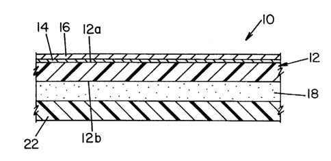
limiting same, FIG. 1 shows a cross-sectional view of a surface laminate 10
illustrating a preferred embodiment of the present invention. Broadly stated,
surface
laminate 10 is comprised of a polymeric film 12 having a first surface 12a and
a
second surface 12b. A thin metallic layer 14 of a flash metal (conventionally
referred
to as a "tiecoat") is applied to surface 12a of polymeric film 12. At least
one metallic
layer 16, preferably formed of copper, is applied to flash layer 14. An
adhesive layer
18 is disposed on surface 12b of polymeric film 12. In the embodiment shown, a
releasable protective film layer 22 is provided on the exposed surface of
adhesive
layer 18.
CA 02360323 2001-07-11
WO 00/55908 PCT/US99/28442
Polymeric film 12 is preferably formed of polyimide and has a thickness of
between 12.5 pm and 125 p.m. Specific examples of materials that may form
polymeric film 12 include Kapton-E or Kapton-HN (manufactured by LE. DuPont),
Upilex-S or Upilex-SGA (manufactured by Ube) and Apical NP (manufactured by
S Kaneka). Flash layer 14 may be formed from metals selected from the group
consisting of chromium, chromium-based alloys, nickel-based alloys, titanium,
aluminum, vanadium, silicon, iron and alloys thereof. Flash layer 14
preferably has a
thickness of between 0~ (none) and 500, and more preferably, between about S0~
to
200A.
As indicated above, metallic layer 16 is preferably formed of copper, and has
a
preferable thickness of between 0.1 pm (10000 and 70 pm. The copper forming
metallic layer or layers 16 may be applied by vacuum-metallization,
electrodeposition,
electroless deposition or combinations thereof on flash layer or layers 14. In
accordance with a preferred embodiment of the present invention, metallic
layer 16 is
electrodeposited onto flash layer 14.
Refernng now to adhesive layer 18, the overall thickness of adhesive layer 18
is preferably between 12.5 pm and 125 Vim. Adhesive 18 is preferably a
dimensionally stable adhesive and may be a B-staged or a partially cured resin
material or a pressure-sensitive adhesive. A product manufactured and sold by
Minnesota Mining and Manufacturing (3M) under the name "High Perfornlance
Epoxy Adhesive Bonding Film" finds advantageous use as the adhesive film in
the
production of the flexible laminate according to the present invention. This
product is
comprised of an epoxy resin and is available in thicknesses of about 1 to 3
mils. The
materials are provided by the manufacturer with removable protective polymer
films
on both surfaces thereof. The material has the following physical properties
as
disclosed by the manufacturer.
Pro ert Units IPC Test
Glass Transition* C 180
CTE 20 -110C ppm/C 60
110 -180C 87
180 - 250C 213
Peel Stren th Lbs.linch 8 2.4.9
Volatile Content % 1 2.3.37
Moisture Absor % 1.7 2.6.28
tion
Chemical Resistance% >90 2.3.2
CA 02360323 2001-07-11
WO 00/55908 PCT/US99/28442
6
Dielectric Constant*__ 3.4 2.5.5.3
Dissi anon Factor* .022 2.5.5.3
Dielectric Stren Volts/mil 2200 D-149
th
Insulation ResistanceMe ohms 1.OOE+06 2.6.3.2
Volume Resistivit Me ohms-cm 5.OOE+07 2.5.17
Surface Resistivit Me ohms 7.OOE+05 2.5.17
Solder Float Pass 2.4.13
Low Tem erature Pass 2.6.18
Flexibilit
Flexural Endurance C cles 1787 3.7.4
Fracture Tou hness M a*m'~ 0.65
Modulus GPa 3.5
Examples of other adhesives that may find advantageous application in the
present
invention as adhesive layer 18 include acrylics, epoxies, nitrite rubbers,
phenolics,
polyamides, polyarylene ethers, polybenzimidazoles, polyesters, polyimides,
polyphenylquinoxalines, polyvinyl acetals, polyurethanes, silicones, vinyl-
phenolics,
urea-formaldehyde and combinations thereof. The adhesive preferably is flame
retardant naturally or has a flame retardant material added to it.
Protective film 22 preferably has a thickess of between 12.5 ~m and 125 pm.
Films that would find advantageous application as a protective film 22 include
fluoroplastics, polyester, polyolefin, polyethylene, polypropylene, polyvinyl
alcohol,
vinyl resin (PVC and PVDC), and mixtures thereof.
According to one aspect of the present invention, laminate 10 is preferably
formed as a individual component for later use in forming a mufti-layer
printed circuit.
FIG. 2 shows a mufti-layer printed circuit 30 having surface laminates 10 as
the outer
1 S surface sections thereof. Mufti-layer printed circuit 30 is generally
comprised of an
inner laminate section 40 that is comprised of two previously formed printed
circuit
laminates S0. Circuit laminates 50 are separated by an intermediate dielectric
layer
62. Each printed circuit laminate SO is comprised of an inner core 52 having
circuit
leads or connectors 54 formed on the outer surfaces thereof. As indicated
above, cores
52 may be reinforced or non-reinforced and may include an epoxy, polyester,
cyanate
ester, bismaleimide triazine, polynorborene, teflon, polyimide or a resinous
material,
and mixtures thereof, as is conventionally known. Printed circuit laminates SO
are
secured to dielectric layer 62, as is conventionally known.
In accordance with the present invention, surface laminates 10 are applied to
inner section 40. Specifically, releasable protective films 22 are removed
from surface
laminates 10 to expose the surface of adhesive layer 18. Adhesive layer 18 is
brought
CA 02360323 2001-07-11
WO 00/55908 PCT/US99/28442
7
into contact with circuit leads 54 of the respective printed circuit laminates
S0.
Depending upon the material used in adhesive layer 18, a permanent bond
between
adhesive layer 18 and circuit leads 54 may be accomplished by heat and
pressure.
The resulting mufti-layer printed circuit 30 thus has outer surface laminates
10
with an exposed metallic layer 16 available for a subsequent etching process
to define
a specific surface path or pattern from metallic layer 16. Importantly, as
indicated
above, because metallic layer or layers 16 may be deposited onto a polymeric
film 12,
the thickness of metallic layer 16 may be extremely thin as compared to
conventional
metallic foil. As indicated above, metallic layer 16 may have a thickness as
low as
0.1 ~.m (1000A). Such thin layers of copper on the outer surfaces of mufti-
layer
printed circuit 30 facilitates forming extremely fine and closely spaced
circuit lines
and patterns by an etching process. In addition, the exposed copper surface of
metallic
layer 16 can be rougher than the typically flat surface of standard copper
foils, thereby
providing increased photoresist adhesion, which also facilitates forming
extremely
fine and closely spaced circuit lines and patterns by an etching process.
Moreover, the
absence of glass fibers (typically found in glass-reinforcing prepregs) makes
for easier
laser drilling of microvias to connect metallic layer 16 with circuit leads 54
on printed
circuit laminates S0. Still further, polymeric materials, such as polyimide,
have better
dielectric properties as compared to conventional glass-reinforced prepregs,
thereby
providing improved electrical performance, such as for example, reduced
attenuation
of high speed signals. Furthermore, the high heat stability of materials such
as
polyimides can provide better resistance to thermal excursions that arise
during the
chip attachment process. Thus, surface laminate 10, as used as an outer
surface layer
in a mufti-layer printed circuit assembly, facilitates the production of more
densely
packed mufti-layer printed circuit boards.
The present invention shall now be described by way of examples.
EXAMPLE 1
A surface laminate 10 according to the present invention is prepared by
applying a strip of the aforementioned 3M High Performance Epoxy Adhesive Film
9002 to a preformed adhesiveless, flexible laminate comprised of a 25 pm
Kapton-E
polymeric film 12 having a 70~ flash layer 14 formed of monel and a 5 ~m
metallic
layer 16 of copper. Heat and/or pressure is preferably used to adhere adhesive
layer
CA 02360323 2001-07-11
WO 00/55908 PCT/US99/28442
8
18 to polyimide film 12. The adhesiveless, flexible laminate material
comprised of
layers 12, 14 and 16 is preferably joined to adhesive layer 18 by means of hot
roll
lamination. The temperature of the rolls is about 140°F. The line speed
is about 9
inches per minute. A protective cover, typically found on 3M's Epoxy Adhesive
Film,
S is maintained as protective film layer 22. The resulting composite has 5 p,m
of copper,
70~ of a monel tiecoat, 25 ~m of Kapton-E polyimide film and about a 50 ~m 3M
Epoxy Adhesive Film in a partially cured state with a 50 pm cover sheet
thereon.
A contemplated method of using surface laminate 10 would be as follows:
1 ) Take a mufti-layer circuit board construction comprised of alternating
inner layers and bond ply layers (either previously laminated together under
heat and
pressure or not) and then lay up with surface laminate 10 on either one or
both sides
after removing protective releasable film 22. Adhesive layer 18 is now
contacting the
mufti-layer circuit board stack.
2) Laminate surface laminates 10 to the mufti-layer circuit board through
conventional laminating techniques.
3) Process the exterior surface of surface laminate 10 to form strip
conductors (i.e., printed circuits) by techniques known to those skilled in
the art to
complete a mufti-layer printed circuit board.
EXAMPLE 2
A surface laminate 10 according to the present invention is prepared by
applying a strip of the aforementioned 3M High Performance Epoxy Adhesive Film
9901 or 9902 onto a previously formed adhesiveless flexible laminate comprised
of a
50 p.m Kapton-E polymeric film 12 having a 701 flash layer 14 formed of monel
and
an 18 pm metallic layer 16 of copper. Heat and/or pressure is preferably used
to
adhere adhesive layer 18 to polyimide film 12. The adhesiveless, flexible
laminate
material comprised of layers 12, 14 and 16 is preferably joined to adhesive
layer 18 by
means of hot roll lamination. The temperature of the rolls is about
140°F. The line
speed is about 9 inches per minute. A protective cover, typically found on
3M's
Epoxy Adhesive Film, is maintained as protective film layer 22. The resulting
composite has l8pm of copper, 701 of a monel tiecoat, 50 p.m of Kapton-E
polyimide
CA 02360323 2001-07-11
WO 00/55908 PCT/US99/28442
9
film and about a 50 pm 3M Epoxy Adhesive Film in a partially cured state with
a 50
~m cover sheet thereon.
A contemplated method of using surface laminate 10 would be as follows:
1) Using techniques known to those skilled in the art, process the copper
side of one or more of the aforementioned composite structures to form a
desired
circuit pattern or circuit leads thereon. Releasable protective film 22
preferably covers
the adhesive layer 18 during such process so as to protect the adhesive from
processing chemicals.
2) Creating desired openings through surface laminate 10 at desired
locations to allow interconnection of metal layers may be done at this time.
The
formation of openings may be by laser ablation or other techniques known in
the art.
3) Creating metal-to-metal interconnections may be done at this time
using techniques known to those skilled in the art.
4) Remove protective releasable film 22 to expose adhesive layer 18 and
align surface laminate 10 with an inner section 40, as described above.
5) Laminate surface laminates 10 to inner section 40 through conventional
laminating techniques.
6) The openings and metal-to-metal interconnections may be made at this
time using techniques known to those skilled in the art.
7) Apply conventional techniques to exterior surfaces of surface laminate
10 to complete mufti-layer printed circuit boards.
The foregoing description is a specific embodiment of the present invention.
It
should be appreciated that this embodiment is described for the purpose of
illustration
only, and that numerous alterations and modifications may be practiced by
those
skilled in the art without departing from the spirit and scope of the
invention. It is
intended that all such modifications and alterations be included insofar as
they come
within the scope of the invention as claimed or the equivalents thereof.