Note: Descriptions are shown in the official language in which they were submitted.
CA 02360534 2007-02-28
1
DIGITAL COMMUNICATION METHOD AND DIGITAL
COMMUNICATION SYSTEM
This invention concerns a system and a process for digital communication.
This invention proceeds from problems as they arise in hearing aid technology.
On the other hand, its proposals for solving them can be generalized, in the
sense that they can basically be used for digital communication between units.
Hearing aid technology is increasingly moving toward processing signals
digitally, especially audio signals, for which a so-called "digital signal
processing"
unit or DSP is used. Depending on the hearing aid configuration, these DSP are
connected to many different, varied and potentially identical peripheral
units,
thus, for example, one or more acoustic/electric converters, T-coils and
controllers, such as potentiometers for adjusting amplification, interface
units,
etc. In the most general cases, such units are analog units in themselves. But
so
they can be connected flexibly to the DSP, A/D converters are integrated into
such analog peripheral units, as they are used on hearing aids, so that the
following will assume that the peripheral units each have outputs for serial
digital
data. Reference is made to PCT/CH98/00502, published under no.
W099/009799.
The invention described in the above patent application proposes, inter alia,
establishing communication between peripheral units and a central digital
processing unit, the DSP, by a three-wire connection system, like for example
an I2S bus and corresponding interface units, like the ones sold by
Philips.
Such a bus configuration has proven extremely worthwhile, inter alia, because
of
its simplicity, in terms of the hardware and software to be installed, and its
energy consumption for hearing aid applications.
CA 02360534 2007-02-28
2
The present invention is thus based on such a three-wire bus configuration, in
which serial digital data SD are transmitted on a data line SD, permission
signals WS on a second line and clock signals SCL on a third line. A system
working with such a three-line bus, as it is used in the above-mentioned
application especially for hearing aids, will be explained using Figure 1
(Prior
Art) as the basis for understanding the invention on which this application is
based.
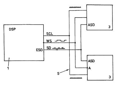
Between a digital signal-processing unit DSP and two peripheral units 3, there
is, apart from electrical feed lines, a three-wire bus connection 5. On the
one line
SCL, the system clock signal is placed, which is usually generated in the DSP
(not shown). On a second line SD, the data-transmission line, or data line for
short, serial digital data from both peripheral units 3 are written and
transmitted
to the DSP, for which the first units have data outputs ASD to output such
data,
and the DSP has a data input ESD.
Usually, a permission signal is placed on the third line WS, the so-called
"word-
select line" by the DSP, and its respective binary state determines when which
of the two peripheral units 3 can write data for the DSP on the common data
line
SD.
Particularly on hearing aids with a bus system, according to Figure 1, there
is a
need, while keeping the advantages of the three-wire bus system, to create two-
way data communication between the DSP and the peripheral units 3, not just
one-way communication from the peripheral units 3 to the DSP, as in Figure 1.
There is another problem with the system in Figure 1. Namely, if the hardware
is
configured, the DSP does not know how many peripheral units - one or two - are
connected, and the one peripheral unit considered 3 "knows" just as little
about
whether it is connected to the bus alone, or whether a second such unit is
connected to the same bus 5: without contact, there is a conflict over writing
CA 02360534 2007-02-28
3
data to the SD; each unit provided considers itself entitled to write data,
for
example in the '1' state of the WS line.
Thus, one aspect of the present invention concerns a method of digital
communicating via a three-wire link among:
a first unit having at least one serial data input and a write select
command output; at least two second units, each having a serial data output
and
a write select command input;
a one-wire serial data communication line interconnecting second unit
serial data outputs and said serial data input;
a one-wire write select command line interconnecting said write select
command output and said second unit write select command inputs;
a clock wire line interconnecting said first and said at least two second
units;
comprising the steps of:
establishing communication from said second units to said first unit by
generating from said write select command output a write select command
signal to said write select command inputs, thereby establishing which of said
second units is allowed to write data on said serial data communication line;
establishing communication from said first unit to said second units by
encoding at said first unit upon said write select command signal on said
write
select command line further data, and decoding said further data from said
write
select command line at said second units.
It should be emphasized that although the procedure in the invention is based
on the fact that two peripheral units can be connected to a DSP unit via the
three-wire bus system mentioned, the invention can be expanded by connecting
more than two peripheral units to the one DSP, as can be seen from the
following description.
Another aspect of the present invention concern a system for digital
communication, comprising:
CA 02360534 2007-02-28
4
a digital processing unit having at least one input for serial digital data
and an output for a write select signal;
at least two removable further units, each with an output for serial digital
data and an input for a write select signal;
removable further unit outputs being connected by a first single-wire line
to said input of said digital processing unit;
said output of said digital processing unit being connected to said
removable further unit inputs by a second single-wire line;
said digital processing unit and said further units being interconnected by
a third single wire line for a clock signal; said digital processing unit
having an
encoder operationally connected to said output for said write select signal to
encode upon a second line further signals;
said two removable further units having each a decoder operationally
connected to said removable further
The second problem mentioned is solved by the fact that - in an initialization
phase - independent, serial digital random signals are applied to the data
line on
the second unit or units connected to it, and it is observed whether a given
signal state occurs on that line which clearly indicates the number of second
units connected.
Although in certain cases, the solution to the first or second problem
mentioned
above may meet the respective need alone, in another much preferred
embodiment of the invention, whether it is the process or the digitally
communicating system, a combination of the solutions mentioned in the
invention to the two problems is proposed.
As was mentioned, the problems on which this invention is based and their
solution come from hearing aid development, considering the miniaturization
and energy problems that exist with hearing aids.
CA 02360534 2007-02-28
Therefore, in another preferred embodiment, the first unit is a digital signal-
processing unit of a hearing aid, and the second units are peripheral units of
the
hearing aid, like especially acoustic/electric converters, electric actuators,
or for
example T coils, controls, like potentiometers or switches, interface units,
etc.
In another preferred embodiment of the invention, the peripheral units work
like
acoustic/electric converters, for example and typically, over a preferably
built-in
A/D converter on the data line.
In another preferred embodiment of the invention, the random signal is
produced
by the fact that the A/D converter working on the data output is given a noise
signal on the input side, but preferably directly uses the quantization noises
of
an LSB (lowest significant bit) on the A/D converter output.
In terms of the solution to the conflict of which second unit can write when
on the
data line, in one much preferred embodiment, the procedure is that only one of
the second units provided can detect the predetermined signal state mentioned
at the same time.
So when that state is detected on only one of the two units connected, then
that
it "knows" that, for example, a second unit is also connected. Thus the
permission phase determined by the permission signal on the permission line
WS for the second unit considered is now inverted, preferably on the second
unit detecting that state first.
At the beginning, the initialization WS='l' is the permission phase, so WS='O'
is
defined as the permission phase on the second unit identifying. Thus, the
second unit identifying acts "different" than or complementary to the second
unit
connected in terms of permission to write data: This resolves the conflict
over
writing data on the same data line SD.
CA 02360534 2007-02-28
6
In one preferred embodi-ment, the signal is detected on the data line at each
second unit and is logically coupled to the random signal given at this unit
prevailing at the same time. The random signals of the second unit connected
are also preferably placed on the data line via a "wired AND" interconnection
and the presence of two second units is indicated when the state of the data
line
is '0', but the state of the random signal assigned to it is '1'.
Because the first unit does not usually tolerate signals on the data-
transmission
line that are not defined electrically for an open input, it can be essential
that a
second unit considered connected also definitively know that there is no
second
one. This is achieved, by the fact that every second unit connected considers
itself alone on the second unit connected to the data line after a given span
of
time has gone by without it having detected the predetermined signal mentioned
itself and without a random signal appearing on the data line in phases of the
permission signal write-locked for it.
In one preferred embodiment on the second unit, which has identified itself as
the only one connected to the data line, in phases write-locked for it, a
defined
electrical potential is now applied to the data line, preferably a potential
corresponding to the logic state V.
This makes it so that in the initialization phase, how many second units, one
or
two, are connected to the common data line is identified without the
cooperation
of the first unit. It also makes it so that if there are two units provided,
the data-
write competency is controlled and if there is only one second unit,
electrical
conditions are produced on the data line that, in any case, meet the
requirements for the first unit.
Thus, the initialization phase mentioned preferably begins by turning on the
electric power to the units mentioned and ends a certain number of SCL cycles
later.
CA 02360534 2007-02-28
7
If more than two second units are connected to a single fit-st unit, then it
remains
so for all units provided, when a common SCL clock line and a common
permission line WS are used, while an additional data line is provided per
other
pair and/or per other initiated pair of the second unit provided. This keeps
it so
that only two second units can write to a common data line, on one hand, and
the advantages of the three-wire bus connection are also used, on the other.
Regarding the identification and conflict resolution described above, if more
than
two second units are connected to the first unit, the configuration
identification
and conflict resolution are logically resolved per data line provided
according to
the invention.
Thus, after a given time span has expired in the initialization phase, the
respective number of second units connected is known on all data lines
provided, and permission to write data is given without conflict.
Particularly when more than two second units are connected to one first unit
and, as mentioned, only one common permission line is working on all second
units provided, it is necessary, if the first unit should communicate with the
second units over the permission line, that the second units connected can be
addressed as receiver stations.
For this purpose, addresses are produced on at least some of the second units
connected by means of random digital signals, and preferably, after the
prescribed initialization phase, by means of those random signals that were
used in the initialization phase for the identification process.
The random addresses of every second unit are read on the first unit and
compared with one another. According to the invention, the first unit orders
all
second units, via the permission line, to generate new random addresses when
at least two of the addresses compared are the same.
CA 02360534 2007-02-28
8
Then, data signals from the first unit, and especially command data, are
produced only within predetermined sections of phases of the permission
signal,
which ensures that no conflicts arise between the permission signals given on
the permission line and the data signals mentioned.
The invention will now be explained by example using other figures.
Figure 2 shows the system in the invention, which is capable of two-way
communication, starting with the view in Figure 1
Figure 3 shows schematically the signal in the invention produced by
superimposing the permission signal and data signal on the permission line on
a
time axis,
Figure 4 shows one preferred embodiment of the output phase of the second
unit in the invention, which works according to the invention, as preferably
also
used on the system in Figures 2 and 3, in the form of a simplified signal
flow/function chart,
Figure 5 is a view similar to Figure 2 of the system in the invention with
more
than two second units that can be connected to a first unit,
Figure 6 is a simplified function/signal flow chart that shows some of the
preferably used output phase of a second unit used in the invention to produce
addresses randomly.
Figure 2 is a schematic view of the system in the invention, which works by
the
process in the invention. The same reference numbers are used as in Figure 1.
Unlike the procedure in Figure 1, DSP1, which is connected to an output for
the
permission line WS, has a coder 10 and peripheral units 3a, 3b with a working
connection to the input for the permission line WS, here a decoder 12.
CA 02360534 2007-02-28
9
Figure 3 shows, on the time axis, the usual cyclic binary permission signal
SWS,
which is put on the permission line WS, as known and according to the known
system in Figure 1. In the one phase, corresponding to I3a, one of the
peripheral units, for example 3a, is authorized to write data on data line SD,
and
in the complementary phase, 113b, the second peripheral unit connected, for
example 3b, is. According to the invention, now within predetermined sections
of
the phase cp of the permission signal SWS by the coder 10 of DSP1 , and as
shown schematically in Figure 3, data DA, especially command data, are
transmitted to the peripheral units 3a, 3b and decoded there in the respective
decoder 12. To address one or if necessary - as will still be explained - more
of
the peripheral units by DSP1 purposefully or selectively, the data DA
superimposed on the SWS signals, if necessary, include call-up addresses for
the corresponding peripheral units 3.
This makes it possible for two-way communication to be established between
the peripheral units and the DSP1 over the three-wire bus connection, on one
hand from the peripheral units to DSP1 over data line SD, and on the other
hand, from DSP1 to the peripheral units 3 over the permission line WS.
Now, if the system hardware is configured according to Figure 1 or - and
preferably - according to Figure 2, one or two peripheral units 3 can be
provided.
If the same permission signals SWS are first fed to the peripheral units 3
connected over the same permission line WS, and both units consider
themselves entitled to write to data line SD first, for example in Phase I, as
in
Figure 3, a conflict arises in terms of permission to write to line SD.
Figure 4 is a schematic view of one preferred design of the output stages
provided in the second aspect of the invention on the system in Figure 1 and,
preferably in Figure 2, on the peripheral units 3. All peripheral units
provided
preferably in this aspect of the invention are built the same as far as the
output
stage shown in Figure 4 is concerned. This is especially true of peripheral
units
CA 02360534 2007-02-28
on a hearing aid built with the system described. One or two peripheral units
3,
bordered by dotted lines in Figure 4, are connected to data line SD.
An A/D converter 14 works with its output A14 on a MOSFET output 16, via
which the output signals A14 of the A/D converter of two units are placed on
data line SD in a "wired AND" circuit.
In the initialization phase, i.e., the phase in which the prevailing hardware
configuration of the system is identified and data-write conflicts are
resolved, the
input of the A/D converter 14 is connected by the effective signal path N to a
noise source, like a resistor 18, for example, as is shown schematically by
10 switch S18, for example. The flipping of switch S18 into the "random
position" is
preferably triggered by first applying the supply voltage to the system (not
shown). At the same time, a timer 15 is triggered. With the A/D converter 14,
a
random generator is produced on the peripheral units connected, hence random
generators independent of one another. First of all, the peripheral units
connected 3 write in the permission phase, for example I in Fig. 3, the
digital
random signals so generated at the same time on the data line SD. In another
much preferred form of embodiment, one or more pair of LSBs of the converter
14 are used as the random signals. Usually, the A/D converter produces a noise
signal on its LSB. In this case, the resistor 18 working as an externally
connected noise source is not necessary, and only the LSBs mentioned at
output A14 are used.
The electrical signal prevailing at that moment on data line SD is picked up
on
each of the peripheral units 3 connected by an inverter 20 and is fed to an
AND
interconnection 22 with the prevailing output signal A14 of the A/D converter
14.
When the output signal of the A/D converter 14 is '1' and the prevailing
electric
potential on the SD lines is '0', this clearly means that a second peripheral
unit is
working on the data line SD, and with an output signal of it's a/D converter,
CA 02360534 2007-02-28
11
which is on '0' at the moment. This state, clearly indicating the presence of
two
peripheral units on the same data line SD, is recorded at interconnection 22
and
stored, as shown schematically with the bistable element 24.
Because of the random signal placed on the data line SD, after a given period
of
time, this clear configuration-display signal stored on bistable element 24
will
appear, with a probability dependent on the length of time selected, if two
peripheral units are connected to line SD. The interconnection 22 makes sure
that only one of the two peripheral units connected 3 can detect the state
mentioned at the same time, so that one of these units will always be the
first to
detect that state.
With the setting of the bistable element 24, i.e., to identify that two
peripheral
units are working on data line SD, the permission signal of line WS acting on
the
enable input E of the A/D converter 14, for example, is inverted on the
identifying peripheral unit, as shown schematically with the switch 25 and the
inverter 26.
Now, permission to write for the identifying peripheral unit 3 is inverted in
terms
of the state formerly prevailing, hence switched to Phase II in Fig. 3, for
example.
On the two identifying units 3 provided, the first unit identifying this has
changed
permission phases, while the second unit provided continues to write data in
the
permission phase previously prevailing, for example I in Figure 3 on line SD.
In
any case, the peripheral unit 3 that does not identify that two such units are
connected and whose bistable element 24 is not therefore on, has no
information on whether a second unit is provided or whether it is the only one
connected.
In many cases, however, it is essential - as explained below - that when only
one peripheral unit is connected, it is identified directly and without doubt.
CA 02360534 2007-02-28
12
Although the unit that has detected the presence of a second unit "knows" that
two units are working on data line SD, on the other hand, a peripheral unit in
which this state was not detected, does not know whether, if necessary, a
second unit has already detected this state and has reacted accordingly or
whether it is actually the only one connected.
If one peripheral unit on the system in Figure 1 or Figure 2 is the only one
connected to data line SD, and writes data at the rate of permission signal
SWS
on permission line WS, the electrical potential of data line SD is not defined
in
phases when writing is not allowed. This is because, as shown with element 21
in Figure 4, output ASD is connected "floating" by signal WS in non-write-
permissible phases. This electrical state of data line SD is generally not
allowed
at the input ESD of DSP1, and usually cannot be considered, because the
systems previously known are designed to work defined with two peripheral
units 3.
One peripheral unit 3 considered is then connected to data line SD as the only
one, if, on the one hand, the bistable element 24, is not set on it, i.e.,
this unit
has not detected the presence of a second peripheral unit and in write-locked
phases of the permission signal, no random digital signal is placed on the
permission line WS on data line SD.
By logically interconnecting the inverted output signal of bistable element
24, the
inverted permission signal on enabling input E of the A/D converter 14 and the
inverted signal on data line SD, according to Figure 4, as on the logic AND
interconnection 30, on the output side of this interconnection, a '1' signal
is then
produced if:
* no second unit was detected on the unit considered (element 24 not set),
and
* the permission signal is in a phase that does not permit this unit, and
CA 02360534 2007-02-28
13
* during this permission phase no random signal is produced on the data line
SD.
If this state is detected, another bistable element 32 is set, whose output is
interconnected to the inverted permission signal SWS at a logic AND
interconnection 34. As schematically with switching element 36, data line SD
is
switched to a defined, for example, reference potential in the write-locked
phases of the unit 3 being considered if that unit is working alone on the
data
line.
This corresponds to placing '0' signals on data line SD.
Now, in the initialization phase described, without DSP1 doing anything, both
is
any write conflict on data line SD ruled out, and it is made sure that if a
single
peripheral unit is connected, even in write-locked phases, a defined
electrical
potential will prevail on data line SD.
As can be seen, communication with DSP1 is not necessary for the
initialization
phase described, for example in Figure 4. The initialization phase mentioned
is
preferably triggered when the supply voltages to the peripheral units
connected
are switched on, and hence also the timer 15 on each peripheral unit, which by
counting, for example 4096 SCL cycles, determines how long the initialization
phase mentioned should last. This time span is measured, especially as
mentioned, for the safe quantity with which it should be detected whether two
peripheral units 3 are connected to the common data line SD.
Thus, it can be seen that the first aspect of the invention, namely creating
two-
way communication, and the second aspect of the invention, namely identifying
the configuration and resolving write-competency conflicts in the
initialization
phase, are independent of one another, but, as will be stated below, can
preferably be combined, especially on a hearing aid with the digitally
communicating system in the invention.
CA 02360534 2007-02-28
14
Figure 5 shows the system in the invention, which is based on the basic system
in FIG. 2, but in which one and the same DSP1' can have any number of
peripheral units 3a, 3b ... 3x connected to it.
In Figure 5, the peripheral units 3x, for example, on a hearing aid with the
system in the invention, made up of microphones, T-coils, potentiometers,
wireless communication sending/receiving units and interface conductors, for
example, are all provided with an A/D converter 14, as shown. Each of these
units works as already explained and is designed, for example, as was shown in
Figure 4. All peripheral units 3x provided are connected to DSP1' via the
common clock line SCL and the common permission line WS. One data line
SD1, SD2, SDy is provided per pair of peripheral units 3x and per pair
started,
according to Figure 5, for the five peripheral units shown, for example, and
hence their three, SD1 to SD3.
Such a system goes through the prescribed initialization phase for each pair
of
peripheral units 3x provided and for each data line SDy.
After the initialization procedure described above is over, there are no more
write conflicts on the data lines, and one of the binary states of the
permission
signal SWg is assigned to the permission line WS of one of the peripheral
units.
Especially with the configuration in Figure 5, in which more than two
peripheral
units are connected to one DSP1', however, there is the problem that the data
transmission in the invention from DSP1 to peripheral units 3x should take
place
on the permission line WS in Fig. 2 or 3.
After the prescribed initialization phase is over, a "generate addresses"
command is given by DSP1' over the common permission line WS, as shown in
Figure 3, which is interpreted the same on all peripheral units connected 3x.
The
CA 02360534 2007-02-28
conclusion of the initialization phase is controlled by the timer 15, which
first
activates the decoding unit 12, as in Fig. 6, for example.
According to Figure 6, the "generate addresses" command placed on permission
line WS is decoded on the now free decoding units 12 of peripheral unit 3,
everywhere so that the A/D converter 14 used as a random generator writes a
random signal sequence on data line SD during a predetermined time t, on one
hand, and at the same time files it in an address memory 409 as a random
address, which forms an address with the permission findings in element 24, as
in Figure 4.
10 With a high degree of probability, based on the independence of the random
generator on all peripheral units 3x, the random addresses filed in the
respective
address memories 40 and placed on the SD at the same time are not the same.
Of course, the respective peripheral units 32 write the random addresses in
the
write permission phases I and II in Fig. 3 of the permission signal on WS
assigned to them in the initialization phase, which is not shown in Fig. 6.
Two peripheral units connected to one data line, for example SD1, always have
different addresses, since the specification of their write permission was
determined in terms of cycles on line WS and is part of the address.
Thus, it is established from the start that clearly addressable peripheral
units are
connected per individual data line considered SDx, since the permission
phase determines the exclusive addresses with the storage state of element 24
in any case. But a case can occur where the address of a peripheral unit
connected to a data line SD is the same as the address of a peripheral unit
connected to another data line SD, hence units with the same write-permission
phase. If this is determined on DSP1, another "generate addresses" command is
triggered, specifically to the peripheral units found to be the same, by their
CA 02360534 2007-02-28
16
common addressing. This goes on until all peripheral units connected have
filed
different addresses in memories 40, 24 and they are also posted in DSP1'.
Because of the independence of the random generators used, this procedure is
also completed in a short time for several peripheral units.
Of course, it is also possible to provide addresses programmed practically
into
the hardware on at least some of the peripheral units provided beforehand, for
example in the ROM.
The process and the communications system described provide a highly simple,
versatile connection based on a three-line bus connection, which is especially
suitable for use in hearing aids.