Note: Descriptions are shown in the official language in which they were submitted.
GR 99 P 1120
Description
CA 02360951 2001-07-26
Method for converting NxSTM-1 signals into STM-N
signals
The invention relates to a method according to
the preamble of claim 1.
As a rule, contemporary transmission methods
are subdivided into transmission methods which transmit
information in accordance with a synchronous transfer
mode (STM) or an asynchronous transfer mode (ATM).
The synchronous transfer mode (STM) is based on
the transmission of information in SDH (Synchronous
Digital Hierarchy) transmission technology. In this
technology, the information is transmitted in frames.
These are subdivided into a control field (SOH, Section
Overhead; POH, Path Overhead) and a container field. In
the former, control information relating to the
connection is transmitted whilst in the latter, payload
is deposited. The payload used can also be ATM cells.
These must then be arranged in the frame structure at
the beginning of the transmission process and removed
again at the receiving end. The control information
considered is, for example, information with respect to
the security of the transmission, bit errors, circuit
failure, clock accuracy, etc.
The control field has two sub-areas SOH and
POH. The sub-area designated by SOH has control
information with respect to a transmission section (for
example between two switching systems) whereas in the
sub-area designated by POH, control information is
transmitted between two subscribers (end-to-end).
The transmission of information by means of the
SDH transmission technology assumes high clock
accuracy. If clock inaccuracies occur during the
transmission process, for
.._..n......~ ~..~.~...~....-....~.~~..~ .-_.......
GR 99 P 1120
CA 02360951 2001-07-26
- 2 -
example due to delay fluctuations, or if different
clock rates are defined due to different situations in
different countries, the received containers become
displaced beyond the frames. A frame can, therefore,
still contain part of the payload of the last container
and part of its own container.
In contemporary synchronous transmission
systems, STM-1 interfaces are used. An STM-1 interface
is physically represented by a connection between two
SDH switching systems. The STM-1 interface is thus the
basis of the SDH transmission. For this reason, the SDH
switching networks arranged in the SDH switching system
are currently designed for switching through STM-1
signals in the prior art.
In future, however, higher-order signals such
as STM-N (N>1) signals are to be transmitted. This
results in circuit switching problems in the SDH
switching networks hitherto used. A method for
bypassing these problems, known in the prior art, is
the Virtual Concatenation Mode. This is a standardized
method by means of which, for example, STM-4 signals
are split into 4 STM-1 signals. During the
transmission, 4 STM-1 signals are thus supplied to the
receiving switch, switched through and then assembled
again to form one STM-4 signal.
In this process, however, the NxSTM-1 signals
pass through different paths in the network. Although
the NxSTM-1 signals are sent out at the same time, they
arrive at different times at the receiving switching
center due to different delays. Converting the STM-1
signals into NxSTM-1 signals, however, requires that
the STM-1 signals arrive at the same time. In the prior
art, storage devices such as, for example, FIFO storage
devices are used for recovering the containers in the
correct order in order to solve this problem. For this
purpose,
.._...~..m._....~,...,~....._".~..~.._.___..-_.... -___ ._ _._._.__.-
~~..~,..~.._....~.....-_ _. . .
GR 99 P 1120
CA 02360951 2001-07-26
- 3 -
the FIFO storage devices must be addressed absolutely
which means increased expenditure since, on the one
hand, the absolute addresses must always be stored
somewhere and on the other hand a +/- area must be
reserved. In practice, this is associated with
increased control expenditure.
The invention is based on the object of
demonstrating an approach to have the STM-1 signals
sent via different paths which can be regenerated and
forwarded in a practical manner at the receiving end.
The invention is achieved by the features
specified in the characterizing clause on the basis of
the features specified in the preamble of claim 1.
The advantageous factor in the invention is, in
particular, a relative dynamic logic operation between
write addresses and read addresses of the FIFO storage
devices. This renders superfluous a continuous absolute
control of the write and read addresses respectively.
Furthermore, such a procedure is associated with a gain
in dynamic range during the conversion process.
Advantageous further developments of the
invention are specified in the subclaims.
In the text which follows, the invention will
be explained in greater detail with :reference to an
exemplary embodiment. In the figures:
Figure 1 shows an SDH container according to the prior
art
Figure 2 shows the container of an STM-4 interface
Figure 3 shows a circuit arrangement on which the
method according to the invention is running
Figure 4 shows the reading of the payload from the
FIFO storage devices according to the method
according to the invention
_. .._~.w~..~.._._.._ ......__ ~...~~..,~._.... ___..._._._ _ ...__
__._...~.._
GR 99 P 1120
CA 02360951 2001-07-26
- 4 -
Figure 5 shows the markers arriving at different times
in the FIFO storage devices.
Figure 1 shows the structure of an SDH
transmission frame. Accordingly, two SDH frames F1, F2
are shown as examples. The control information is
deposited in the control fields SOH, POH. The payload
is transmitted in a container CON. According to the
exemplary embodiment above, this is intended to be a
virtual container VC-4. This means that the payload
transmitted here is transmitted at a payload bit rate
of 149 Mbit/s.
A frame is built up of a total of 9 rows. The
control field SOH has a width of 9 bytes per row. The
container CON exhibits a width of 260 bytes per row and
the control field POH has 1 byte per row. Overall, this
results in a magnitude of 2,430 bytes (9x(9+1+260)),
for one SDH frame, 2340 bytes being provided for
transmitting payload.
The start of the container CON in the relevant
frame is designated by a marker Jl. The position of the
marker J1 is stored in a special pointer field Hl, Hz,
H3 of the control field SOH which forms a pointer. This
pointer points to the position of the marker J1. The
control information deposited in the cantrol field SOH
is always deposited at the same place. The container
CON can migrate beyond the frame boundaries F1, F2 due
to clock inaccuracies. The same thus also applies to
the control field POH. In figure 1, the marker J1 marks
the start of the container CON of the frame F1. The
start of the container of the frame F2 is defined by
another marker J1 of frame F2. Thus, the payload
contained in the container of frame F1 is also part of
frame F2 beyond the frame boundaries.
GR 99 P 1120
CA 02360951 2001-07-26
- 5 -
Figure 2 shows the conditions for an STM-4
interface. The STM-4 signals have here been split into
4 STM-1 signals. Here, too, the containers migrate
beyond frame boundaries due to clock inaccuracies. The
beginning of the individual containers is shown by 4 J1
pointers belonging to the frames Fl...F4 in figure 2.
The origin of this is that, although the 4 STM-1
signals have been sent out at the same time, they have
experienced delay differences along the respective
paths . For this reason, these signals also have become
stored in different storage areas of the FIFO-type
buffer stores. Converting the 4 STM-1 signals back into
one STM-4 signal requires time-synchronous conversion
since only this ensures the STM-4 signal..
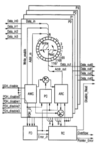
Figure 3 discloses a circuit arrangement by
means of which the restoration of an STM-4 signal from
4 STM-1 signals is achieved. Accordingly, 4 interface
devices Po...P3 are shown. Each of these 4 interface
devices Po...P3 is used at the receiving end to
terminate the connecting line via which the STM-1
signal is transmitted in each case. Since the control
data transmitted in the control fields SOH, POH are
specific to STM-1, this information must be suppressed
during the conversion into an STM-4 signal.
At the input end, the 4 interface devices
Po...P3 are supplied with the STM-1 signals
Data inO...Data in3. The interface device Po is thus
supplied with the STM-1 signals Data_in0, the interface
device P1 is supplied with the STM-1 signals Data inl,
etc. These STM-1 signals are then checked to see
whether the incoming information is payload or control
information. In the control field SOH, an alignment
word is also transmitted to which the frame
synchronizes in each case. If this alignment word is
received, a signal SOH disable is activated and
supplied to the relevant interface device. The third
word in the control field SOH is a pointer which points
to the
..T._,_...~...,~..~._~....-_..- -..,.~...m.~._..r-...-....~
._._.....___~~,~,~.~.,.._. ....._.. _.
a
GR 99 P 1120
CA 02360951 2001-07-26
- 6 -
marker J1. If this is detected, a signal POH disable is
activated and this is also supplied to the relevant
interface device.
Furthermore, each of the 4 interface devices
Po..P3 has a cyclic circular buffer R. This is
constructed as Random Access Memory (RAM) and has the
function of a FIFO store. As a rule, this circular
buffer R is worth in each case 1170 bytes as one half
of a container CON. Furthermore, a counter AWC in which
the payload bytes are counted as determined by the
state of the signal SOH_disable is in each case
provided in each of the interface devices. When both
signals SOH disable, POH disable are inactive, this
count is read out and supplied to the circular buffer R
via a signal addr-in. At the same time, a signal
write_enable is supplied. The count of the counter AWC
thus reproduces the memory address in the circular
buffer R at which the relevant payload bytes are
stored. Furthermore, a counter PC which is incremented
by the incoming payload bytes on detection of the
marker J1 is provided in each of the 4 interface
devices Po...P3. In a further counter ARC, which is also
arranged in each of the 4 interface devices Po...P3, the
address of the circular buffer R under which the
payload bytes are read out again is stored as
determined by the count of the counter AWC, PC.
The devices PD, RC are used as higher-level
devices of the 4 interface devices Po . . . P3 . The former
is a monitoring device which determines whether the
markers J1 of all four interface devices Po...P3 have
been detected. The device RC is a higher-level control
logic which controls and monitors the read processes.
GR 99 P 1120
CA 02360951 2001-07-26
In the text which follows, the operation of the
circuit will be briefly explained:
The STM-1 signals data_in0...data_in3 are
accepted by the relevant interface device. If the
signal SOH disable is inactive, the counter AWC
activates a signal write-enable. At the same time, the
counter AWC is incremented by the number of incoming
payload bytes. The value obtained in this manner is
supplied to the circular buffer R via a signal addr_in
and is interpreted as address by the buffer. The data
data in are deposited in the circular buffer R as
determined by this address. Due to the logical OR
operation on the signals SOH,disable, POH disable
(write enable), only payload is transferred into the
circular buffer R. The information stored in the
control fields SOH, POH is thus suppressed.
On start-up, the signals POH J1 of all interface
devices Po. . .P3 are set to "0" . If the signaling signal
for the marker J1 of the relevant interface device is
detected, the counter PC is started by the signal
POH disable. The signal POH J1 of the corresponding
interface device is then set to a logical "1" or
"high". As long as the signal POH J1 assumes the state
of logical "1", the payload bytes are counted. If the
markers J1 have been received by all interface devices
Po...P3, all signals POH J1 are then set to a logical
"1". As a result, the monitoring device PD initiates
logic operations and forms the difference between the
counts AWC and PC, decremented by 1 and loaded into the
counter ARC. The monitoring device PD then sets all
signals POH J1 to 0 for the next cycle. Furthermore, if
the counts of the counters AWC and ARC are equal, the
read process is stopped in all interface devices and a
signal disable_read is generated because there is no
payload in the circular buffer R
__.__ .. ..._.. _..,.,.,.,_ ~.._....__..__.._......._..___ ..____ ._
..~....~. .~..~...~.. _... ._...~.
A
GR 99 P 1120
CA 02360951 2001-07-26
_ g _
in at least one of the interface devices Po . . . P3.
In detail, the following procedure is adopted:
The counts of counters AWC and PC are
determined. The difference between the two counts is
decremented by 1 and the result is stored in the
counter ARC. At the instant at which all markers J1 have
arrived, the relative delay difference of the STM-1
signals with respect to the STM-1 signals which have
arrived last is thus given in the counter PC.
The counters ARC of all interface devices are
then triggered to transfer the content to the circular
buffer R via in each case one signal addr out. The
latter interprets this value as an address. The data
stored under this address are read out and forwarded as
STM-4 signal as output data data out.
The corresponding conditions are reproduced in
figure 4. Accordingly, the 4 cyclic circular buffers R
of the 4 interface devices R (Po) . . .R (P3) are shown. As a
- last marker, marker Jl of the interface devices P1 has
arrived, for example. All counters are then stopped.
Subsequently, the relative address to the markers J1
which are stored in the remaining 3 interface devices
is then formed. In the case of the interface devices
R(Po) the difference is 6 payload bytes. In the case of
the interface device P2, the difference is 8 payload
bytes and in the case of the interface device P3, the
difference is 17 payload bytes. Triggering the higher-
level logic device RC, the payload is read out and
supplied to an STM-4 frame FR which regenerates 1 STM-4
signal from the 4 STM-1 signals.
.~.....-.~.,- ..~._.~ ______.__._ .
a
GR 99 P 1120
CA 02360951 2001-07-26
- 9 -
The precondition for this method is that the
markers J1 of all STM-1 signals arrive within a half
VC-4 period. The corresponding conditions are shown for
the example of 4 STM-1 signals in figure 2. The markers
J1 are placed within the VC-4 period. For this reason,
the interface circuits can synchronize without
additional signal evaluation. For example, marker J1 of
frame F3 of interface device P3 arrives first, for
example, as described for figure 2. The counter PC is
then started and counts up to 1170. If no further
markers J1 of the remaining containers CON are detected
until then, all counters PC and all signals POH_J1 are
reset and synchronization recommences correctly with
marker J1 of frame F1 at the next cycle.
According to the present exemplary embodiment,
it has been assumed that the magnitude of the delay
differences is smaller than one half container period
of a virtual VC-4 container. However, delay differences
greater than one half container period of a virtual
VC-4 container can also be treated with a modification
of the method.
The interface device according to figure 3 can
still synchronize if the payload in the container is
structured. In this case, the circular buffer R must be
enlarged in accordance with the greatest delay to be
expected. The corresponding conditions are shown in
figure 5. This is the case, for example, if the payload
consists of ATM cells, frame relay ar TCP/IP data.
Because of such transmission formats, synchronization
can be carried out because error-free transmission is
detected by the control field SOH and in this case the
headex of the cell is detected and evaluated by an
additional payload synchronization circuit
corresponding to the transmission format. The
synchronization circuit is designated by HSC in
figure 5. The synchronization can be restored by
__ .~...,~...~.~.,~.._.-,~._. __.._....
GR 99 P 1120
CA 02360951 2001-07-26
- 10 -
combining the pointers of 2 or more VC-4 containers (4
pointers in the case of STM-4) until the payload
synchronization circuit HSC acquires lock. The
combination can be obtained from a simple addition of
2340 bytes in the counting devices of the counters
ARC - triggered by a device J1CL (J1 combining logic)
since, when a number of markers J1 is found, the frame
to which this marker belongs cannot be reliably
detected. The difference between 2 markers J1 of the
same interface device is 2340 payload bytes. After the
payload synchronization circuit HSC has acquired lock,
the markers J1 will not be combined because only jumps
of 3 bytes are allowed according to the SDH standard,
unless the system is re-initialized.
..~.. _--.._._.....~........,......~....._.._.._ __ _. .