Note: Descriptions are shown in the official language in which they were submitted.
CA 02361050 2001-06-O1
WO 00/34203 PCT/US99/26568
High Purity, Siliconized Silicon Carbide Having High Thermal Shock
Resistance
The manufacture of semiconductor devices such as integrated circuits typically
involves heat treating silicon wafers in the presence of reactive gases at
temperatures of
from about 250 °C to over 1200°C. The temperatures and gas
concentrations to which
these wafers are exposed must be carefully controlled, as the ultimate devices
often
include circuitry elements less than 1 um in size which are sensitive to
minute variations
in the wafer processing environment.
The semiconductor manufacturing industry has typically used either horizontal
or vertical carriers made of silicon carbide or siliconized silicon carbide as
kiln furniture
for the wafers, and these carriers have been designed to hold up to about 50
wafers.
When such conventional carriers are used, the processing steps generally
involve fairly
slow ramp rates of between about 10 °C and 30 °C/minute.
However, because of increasingly strict wafer performance and efficiency
requirements, the industry has been considering adopting Rapid Thermal
Processing
(RTP) wafer processing techniques. According to US Patent No. 4,978,567
("Miller"),
under RTP conditions, the wafers are treated in an environment whose
temperature rises
from room temperature to up to about 1400°C in a period of time on the
order of
seconds. Typical RTP ramp rates are on the order of 600-6000 °C/minute.
Under such
extreme processing conditions, the thermal shock resistances of the materials
in this
environment are of critical importance.
Miller discloses RTP wafer carriers made of stand-alone CVD silicon carbide,
and carriers made of graphite coated with CVD silicon carbide. However, the
cost of
stand-alone CVD silicon carbide is often prohibitive, while carriers made of
graphite
coated with CVD silicon carbide suffer from a significant mismatch of
coefficients of
thermal expansion ("CTE") which makes the composite susceptible to thermal
shock.
Siliconized silicon carbide has been considered as a candidate material for
kiln
furniture in RTP systems. In particular, US Patent No. 5,514,439 ("Sibley")
has
disclosed RTP kiln furniture in which siliconized silicon carbide is the
material of
choice. However, in one test involving a commercially available siliconized
silicon
carbide ("Si-SiC") material commonly used as kiln furniture in conventional
wafer
1
CA 02361050 2004-O1-16
processing, it was found that this Si-SiC material lost 40% of its flexural
strength (from
261 MPa to 158 MPa) when subjected to a thermal quench test in which the
temperature
of the environment surrounding the material dropped from 500°C to
0°C nearly
instantaneously.
The finding that the above-mentioned siliconized silicon carbide does not have
outstanding thermal shock resistance in RTP environments is not surprising.
Torti et al,
in "High Performance Ceramics for Heat Engine Applications", ASME 84-GT-92,
discusses another siliconized silicon carbide material (NC-430) made by a
reaction
bonding process which reportedly has high thermal shock resistance. However,
Torti et
al. also disclose that this NC-430 material has a Tc value of only
275°C, which appears
to mean that a significant strength reduction occurs if this material is
instantaneously
subjected to a temperature differential of only 275°C. Weaver et al. in
" High Strength
Silicon Carbide For Use In Severe Environments" (1973) [published in
proceedings of
"International Conference on SiC - 1973, Miami Beach, Florida] reports that a
hot
1 S pressed SiC material comprising 95-99% SiC has a poor thermal shock
resistance.
Therefore, there exists a strong need for a siliconized silicon carbide
material
which has a thermal shock resistance suitable for its use in kiln furniture
designed for
RTP applications.
In addition to the more strict thermal shock requirements, another trend in
the
semiconductor manufacturing industry has been the steady decrease in the level
of
acceptable metallic contamination in the processed wafers. Accordingly, the
industry
has concurrently required the kiln furniture to be made of increasingly higher
purity
materials.
As it is known that the "converted graphite" type of silicon carbide has very
low
levels of metallic contamination, the art has considered making SiC kiln
furniture from
converted graphite materials. The process of making such converted graphite
materials
involves exposing a porous graphite body to Si0 gas under carefully controlled
conditions which allow a 50% replacement of carbon atoms in the graphite
matrix with
silicon atoms and the ultimate production of a stoichiometric beta-SiC body.
JP Kokai
Publication No. 1-264969 (1989) ("Tanso") teaches siliconizing one 30% porous
SiC
material made from converted graphite to essentially full density, and using
that
siliconized material as a wafer boat in semiconductor wafer processing
operations.
Tanso further teaches that its essentially non-porous siliconized product made
from its
2
CA 02361050 2004-O1-16
process can have a density of from 2.9 g/cc to 3.2 g/cc. Since silicon and
silicon carbide have
respective densities of 2.33 g/cc and 3.21 g/cc, respectively, Tanso appears
to disclose
siliconized SiC products having from 64 vol% to 99 vol% silicon carbide.
However, the
actual enabling technology disclosed by Tanso appears to be limited to only
lower SiC
fraction bodies. In particular, Tanso teaches that the reason for its
successful conversion of
graphite to stoichiometric SiC was its decision to limit the density of the
graphite starting
body to no more than 1.50 g/cc in order to provide enough porous passages
within the
graphite body to allow complete infiltration of the Si0 gas. Since following
this suggestion
appears to limit the density of the converted SiC body to only about 2.25
g/cc, Tanso appears
not to teach how to make a converted graphite SiC body having a density of
over 2.25 g/cc
(or 70.09 vol % SiC), and so does not further teach a siliconized SiC body
having over 70.09
vol% SiC.
Poco Graphics Inc., a known commercial producer of converted graphite for use
in
semiconductor wafer processing offers a porous beta-SiC material made from
converted
graphite and having a density of 2.55 g/cc, or about 80 vol% SiC. However, the
reported
room temperature flexural strength of this material (25 ksi, or about 175 MPa)
is relatively
low. Typically, a room temperature flexural strength of at least about 230 MPa
is highly
preferred for commercially useful SiC diffusion components. Moreover, although
it is known
that siliconizing a porous SiC body typically enhances its strength,
information from the
above-mentioned producer discourages siliconizing this porous converted
graphite product
having 80 vol% SiC for fear of thermal expansion mismatch consequences. In
particular,
according to the producer, the difference in the coefficients of thermal
expansion ("CTE")
between silicon (CTE=2.5 - 4.5 x 10⁻⁶ / °C) and silicon carbide (CTE =
4.8 x 10⁻⁶ / °C) is so
great that, on cooldown from siliconization, the SiC contracts much more than
the silicon,
and this creates stresses of the intergrain bonds in the SiC during both
cooldown from
siliconization and subsequent thermal cycles. Therefore, it appears the
information actively
discourages the siliconization of porous converted graphite products having
over 71 vol%
SiC for fear of producing strength-degrading cracks in the composite material.
Therefore,
there is a further need for a siliconized silicon carbide material having over
71 vol % silicon
carbide (preferably over 75 vol% SiC, more preferably at least 80 vol% SiC)
which has both
the higher purity and adequate strength needed for conventional wafer earner
3
CA 02361050 2004-O1-16
applications, and preferably the high thermal shock resistance required for
RTP applications of
the future.
The present inventors ignored the teachings of the above-mentioned producer
information and successfully siliconized the porous converted graphite SIC
product having
about 80 vol% SiC. It was found that the siliconized SiC body so produced was
essentially fully
dense and had a room temperature strength (266 Mpa) which was essentially
equivalent to one
commercial Si-SiC material routinely used as kiln furniture in the
semiconductor processing
industry. Therefore, this new siliconized SiC body comprising converted
graphite fulfills the
desires of today's semiconductor manufacturers for both the high purity and
acceptable strength.
Moreover, the commercially adequate room temperature strength of this material
is surprising in
light of the warnings provided by the information of the manufacturer of the
porous converted
graphite SiC material.
The present inventors further examined the new siliconized material and found
that it
was essentially unaffected by a severe thermal shock test. In particular, when
subjected to the
thermal quench test in which the temperature of the environment surrounding
the material
dropped from 500°C to 0°C nearly instantaneously, the subsequent
MOR strength of the material
dropped by less than 10%. Therefore, this new siliconized SiC body comprising
converted
graphite fulfills the desires of tomorrow's semiconductor manufacturers for
both the high purity
and the high thermal shock resistance needed for RTP applications. Moreover,
the superior
thermal shock resistance of this new material is surprising in light o~
(a) the warnings provided by the producer information of the manufacturer of
the
porous converted graphite SIC material, particularly as they relate to thermal
stresses produced by siliconization,
(b) the failure of conventional Si-SiC products to adequately survive the
500°C
thermal shock test, and
(c) the essential similarity in room temperature strengths and 300°C
thermal shock
test performance between the commercial Si-SiC product and the new material.
It was also found that the material of the present invention possessed a high
temperature
(1300°C) flexural strength which was superior to the commercial
siliconized SiC material.
4
CA 02361050 2001-06-O1
WO 00/34203 PCT/US99/26568
Therefore, in accordance with the present invention, there is a provided a
process
for making a high strength, thermal shock resistant, high purity siliconized
silicon
carbide material, comprising the steps of
a) providing a porous converted graphite SiC body having at least 71 vol% SiC,
and
b) siliconizing the porous converted graphite SiC body to essentially full
density
to produce a siliconized silicon carbide composite body.
Preferably, step a) is achieved by i)) providing a porous graphite body, and
ii)) exposing
the porous graphite body to a reactant in a manner sufficient to produce a
porous
converted graphite SiC body having at least 71 vol% converted graphite SiC.
Also in accordance with the present invention, there is provided a high
strength,
thermal shock resistance, high purity siliconized silicon carbide composite
material, the
material having at least about 71 vol% converted-graphite silicon carbide
matrix having
open porosity, wherein the open porosity of the SiC material is filled with
silicon.
Also in accordance with the present invention, there is provided a
semiconductor
manufacturing kiln furniture component, preferably in the form of a component
suitable
for use in RTP applications, wherein said component comprises the high
strength,
thermal shock resistance, high purity siliconized silicon carbide material
discussed
above.
Also in accordance with the present invention, there is provided a method of
using a semiconductor wafer manufacturing kiln furniture component, preferably
in the
form of a component suitable for use in RTP applications, wherein said
component
comprising the high strength, thermal shock resistance, high purity
siliconized silicon
carbide material discussed above, comprising the steps of
a) providing a kiln furniture component (preferably in the form of an RTP
component) of the new high strength, thermal shock resistance, high purity
siliconized silicon carbide material discussed above, and
b) exposing the component to a reactive gas used in semiconductor
manufacturing in an environment having a peak temperature of from about
800°C to 1400°C (from about 1200°C to 1400°C in
some embodiments).
5
CA 02361050 2001-06-O1
WO 00/34203 PCT/US99/26568
In some RTP embodiments, the temperature of the environment rises from about
room
temperature to the peak temperature at a rate of at least 100 °C/minute
(preferably, at
least 600 °C/minute).
Figure 1 is a photograph of a prior art microstructure of an unsiliconized
porous,
converted-graphite SiC body.
Figure 2 is a photograph of a prior art microstructure of a siliconized SiC
body
comprising fine and coarse alpha-SiC grains.
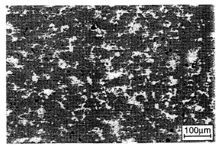
Figure 3 is a photograph of the present invention, a microstructure of a
siliconized
converted graphite SiC body.
Figure 4 is a graph comparing the maximum lengths of silicon pockets in the
material of
the present invention and a competitive prior art material.
Figure 5 is a graph comparing the relative areal sizes of silicon pockets in
the material of
the present invention and a competitive prior art material.
In one embodiment of making the present invention, a commercially available
porous converted graphite material having at least 71 vol% SiC is siliconized.
One
suitable commercially available porous converted graphite SiC material is
SUPERSiCR,
marketed by Poco Graphite, Inc. of Decatur, TX. This material is a porous SiC
made of
converted graphite comprising about 80 vol% beta-SiC. The SiC microstructure
of a
converted graphite body retains the general look of a graphite microstructure
and so is
unique among SiC microstructures and is well-known to the skilled artisan. A
photomicrograph of this material is shown in Figure 1. The microstructure is
characterized by an essential absence of discrete particles. It also has more
substantial
necking than comparable conventional porous SiC bodies made from a bimodal
mixture
of SiC powders. It further has fewer large reservoirs of silicon pockets than
the
comparable bimodal SiC bodies. In general, the absence of coarse SiC
particles, the
higher degree of necking, and the relative absence of large silicon pockets
makes the
structure of the converted graphite body much more homogeneous than the
comparable
recrystallized bimodal SiC bodies. Preferably, the porous graphite starting
material has
a total metallic impurity content of less than 10 ppm.
It is believed that any converted graphite material having an acceptable
amount
of continuous porosity to allow for suitable silicon infiltration may also be
used as a
6
CA 02361050 2004-O1-16
starting material for siliconization. The porosity of the converted graphite
material needs
to be in the range of 5 vol% and 29 vol%. If the material has less than 5 vol%
porosity,
then the porosity is considered to be closed and essentially no infiltration
can be
expected. More preferably, the material has between S vol% and 25 vol%
porosity, and
75-95 vol% SiC. In this range, the degree of porosity typically easily allows
the
essentially complete infiltration of the porosity by silicon, and the vol% of
SiC is high
enough to produce a strong composite. Most preferably, the material has
between 15
vol% and 25 vol% porosity. Typical converted graphite materials contain less
than 10
ppm total metallic impurity and less than 0.1 ppm iron impurity.
In another embodiment of making the present invention, a porous converted
graphite body is first produced. In this embodiment, the porous graphite body
is then
converted to a porous stoichiometric SiC body having at least 71 vol% SiC.
Conventional procedures for making converted graphite may be followed. One
known
method for making converted graphite is disclosed in US Patent No. 4,900,531.
If the converted graphite body is made at a low temperature, it may be
desirable
to recrystallize the porous SiC body at a temperature of at least 1600°
C prior to
siliconization in order to provide more necking to the body.
The siliconization of the converted graphite material may be undertaken in
accordance with the typical siliconization of porous recrystallized silicon
carbide bodies.
Conventional procedures are disclosed in US Patent 3,951,587. For example, in
one
instance, chunks of solid semiconductor-grade silicon are placed in a furnace
near the
porous converted graphite body, and the temperature of the furnace is raised
past the
melting point of the silicon. The molten silicon then wicks through the porous
SiC body
and provides complete siliconization. In other embodiments, the process for
siliconization disclosed in US Patent 4,795,673 ("Frechette") is used.
Without wishing to be tied to a theory, it is hypothesized that some
recrytallization of the converted graphite SiC microstructure may occur during
siliconization (thereby enhancing the degree of interparticle SiC bonding (or
"necking")
and producing a stronger material) if the siliconization proceeds at
temperatures above
about 1600° C. Therefore, in preferred embodiments, the converted
graphite is contacted
7
CA 02361050 2001-06-O1
WO 00/34203 PCT/US99/26568
with molten silicon at a temperature of at least 1600 °C (preferably at
least 1700 °C, and
more preferably at least 1800 °C) in order to promote necking.
Preferably, the siliconized silicon carbide composite body produced in
accordance with the present invention comprises a SiC matrix of converted
graphite
having porosity which is essentially filled with silicon, wherein at least 71
vol% of the
body is SiC. Preferably, at least 75 vol% of the body is SiC, more preferably
at least
80%. Since the porous converted graphite starting materials must also have
adequate
porosity to allow for its complete siliconization, in preferred embodiments,
the
composite has between 75 vol% and 95 vol% SiC and between 5 vol% and 25 vol%
silicon. One especially preferred embodiment has about 80 vol% converted
graphite
SiC. Typically, silicon essentially fills the porosity of the converted
graphite SiC matrix,
preferably resulting in a composite having no more than 4 vol% final porosity,
more
preferably less than 2 vol% final porosity, more preferably less than 1 vol%
final
porosity. In other words, the composite has a density which is at least 96%,
preferably at
least 98% of theoretical density, more preferably at least 99% of theoretical
density.
The SiC microstructure of the composite retains the general look of the porous
converted graphite SiC starting material and so is again unique among SiC
microstructures and is well-recognizable to the skilled artisan. One
photomicrograph of
the siliconized converted graphite structure is shown in Figure 3. Since the
typical
conversion of graphite produces essentially beta-silicon carbide, essentially
all (i.e., at
least 90%) of the SiC in this composite is typically beta-silicon carbide. It
is known that
beta-SiC is a cubic phase, and that a cubic phase material will generally
produce an
isotropic response. In contrast, alpha-SiC is a hexagonal phase and so is
expectedly to
produce responses which are more anisotropic. Since it is known that there is
a thermal
expansion mismatch between silicon and SiC, the isotropic response of the
material of
the present invention to this mismatch may dampen the stresses produced
therefrom,
thereby yielding a higher strength. Therefore, in preferred embodiments, the
SiC is at
least 90 vol% beta-SiC. Accordingly, in some embodiments, the converted
graphite
SiC comprises at least 90 wt% beta-SiC and the step of siliconizing is
performed at a
temperature low enough to prevent substantial conversion of the converted
graphite
beta-SiC and the composite body comprises at least 90 vol% beta-SiC.
8
CA 02361050 2001-06-O1
WO 00/34203 PCT/US99/26568
Nonetheless, it is contemplated that higher temperature graphite conversion or
siliconization processes may be used, thereby partially or fully converting
the beta-SiC
to alpha-SiC.
Preferably, less than 10 wt% of the SiC is characterized as SiC particles
having a
size greater than 30 microns (more preferably less than 5 wt%). Without
wishing to be
tied to a theory, it is believed that a reason for the superior thermal shock
resistance of
this new material may lie in it having essentially no coarse SiC particles. In
particular,
whereas the SiC fractions of the above-discussed NT-430 and the commercial Si-
SiC
materials each possessed about 50 wt% silicon carbide grains having a grain
size of
between 10 and 150 um, the new material has essentially no SiC grains more
coarse
than 30 microns. It is believed that the significant difference in thermal
expansion
coefficients of silicon and SiC grains in these prior art materials causes
stress
concentrations around the SiC grains during the cooling of the composite after
siliconization. However, it is further believed that the spheres of influence
of the stress
produced by the more coarse SiC grains is much larger than the spheres
produced by the
smaller SiC grains. Simply, the more coarse SiC grains have increased
importance in
thermal stress situations. The elimination of the larger and potentially more
harmful
SiC grains from the siliconized material may reduce the critical sphere of
influence of
stress concentration produced by cooling (thereby increasing the mechanical
properties
of the siliconized material) may have been critical to the present invention.
If the elimination of coarse SiC grains is the reason for the improved thermal
shock resistance of the new material, this fording is surprising in light of
the essential
similarity in the room temperature strengths of the commercial siliconized
silicon
carbide material and the new material, and the apparent resistance of the
conventional
material to 300°C thermal shock testing. In particular, if coarse SiC
particles have a
strong effect on room temperature MOR and thermal shock characteristics, then
there
should also have been significant differential stresses in the siliconized
bodies produced
upon their cooling after siliconization, and these stresses might have been
reflected in
differing results in the room temperature and 300°C thermal shock tests
as well. That a
notable performance difference between these materials appears only in the
500°C
thermal shock test is evidence that the effect is quite subtle.
9
CA 02361050 2001-06-O1
WO 00/34203 PCT/US99/26568
Also, if the elimination of coarse SiC grains is the reason for the improved
thermal shock resistance of the new material, this finding is surprising in
light of the
well known fact that coarse grains often act as crack deflectors which
increase the
toughness of the ceramic body. Since it is known that thermal shock resistance
is
enhanced by increasing the toughness of the material, it was considered that
the
elimination of the coarse grains could have reduced the toughness of the
material and
thereby reduced its thermal shock resistance.
Although not particularly desired, the composite may contain additional SiC
particles (for example, present in an amount of between l and 33 vol%) which
were
either infiltrated into the porous beta-SiC body prior to siliconization, or
infiltrated into
the porous SiC body at the time of siliconization.
The chemical properties of the composite body were measured and are as
follows: The total metallic impurity content of the composite material (as
measured by
any conventional method such as GDMS or slurry ICP) is typically no more than
10
ppm, preferably no more than 5 ppm, more preferably no more than 1 ppm. The
iron
impurity content of the composite material (as measured by GDMS or slurry ICP)
is
typically no more than 1 ppm, preferably no more than 0.5 ppm, more preferably
no
more than 0.1 ppm. The titanium impurity content of the composite material (as
measured by GDMS or slurry ICP) is typically no more than 3 ppm, preferably no
more
than 1 ppm. The aluminum impurity content of the composite material (as
measured by
GDMS or slurry ICP) is typically no more than 5 ppm, preferably no more than 1
ppm,
more preferably no more than 0.5 ppm. In comparison, the conventional
siliconized
SiC material has about 80-100 ppm total metallic impurity and about 1 ppm iron
impurity.
Preferably, the composite of the present invention has a thermal conductivity
of
at least 85 W/mK at 400°C, and of at least 50 W/mK at 800°C. The
superior thermal
conductivity of the material of the present invention at high temperatures is
demonstrated in Table II below, which reveals values which are about 10-15%
higher
than those of the.commercial siliconized SiC material. It is possible that the
somewhat
higher thermal conductivity of the siliconized converted graphite material is
the cause of
its superior 500 °C thermal shock resistance. When a material is
thermally shocked, its
survival depends in part upon its ability to quickly dissipate heat, thereby
minimizing its
CA 02361050 2001-06-O1
WO 00/34203 PCT/US99/26568
internal temperature gradients. It is possible that the higher thermal
conductivity of the
material of the present invention allows it to more quickly and evenly
dissipate heat,
thereby minimizing the stress-inducing temperature gradient typically
associated with
thermal shock failure.
However, it is further noted that although the thermal conductivity of the
material of the present invention is higher than the commercially available
siliconized
material, it is only about 10-15% higher. Therefore, it is hypothesized that
the practical
effect of this moderate increase in thernzal conduction is subtle and is only
revealed
under certain conditions in which the 10-15% difference is critical. For
example, while
the 10-15% difference does not appear to make a difference in the 300
°C thermal shock
test (reported in Table I below), it appears to make a great deal of
difference in the 500
°C thermal shock test. To the extent that the apparently similar
performance of these
materials in a 300 °C thermal shock test provides an expectation of
similar results in
higher temperature tests, the superior 500 °C thermal shock resistance
of the material of
the present invention is surprising.
As noted above, the superior thern~al conductivity of the material of the
present
invention is demonstrated in Table II below as being about 10-15% higher than
that of
the commercially available siliconized SiC. Since SiC has a significantly
higher thermal
conductivity than silicon (by almost an order of magnitude), it is clear that
the
dissipation of heat in these bodies is likely carried out mainly by its
conduction through
the SiC phase. However, since each of these materials contains about 80 vol%
SiC, the
difference in thermal conductivity between these two materials can not be
explained
solely on the basis of any difference in SiC content. Rather, it is believed
that the
superior thermal conductivity of the material of the present invention may be
due to the
higher connectivity of its SiC phase (as compared to the conventional SiC
material).
Analysis of the material of the present invention revealed that its SiC phase
is fairly
continuous throughout its microstructure. In other words,.the "veins" of the
SiC phase
are relatively and uniformly thick. In contrast, the commercially available
siliconized
SiC material is essentially characterized by coarse SiC particles partially
connected to
each other by smaller recrystallized SiC particles which are not as wide as
the vein
thickness of the converted graphite material of the present invention. In
other words, the
commercial material has a low degree of necking. Thus, it is possible that
heat is more
11
CA 02361050 2001-06-O1
WO 00/34203 PCT/US99/26568
easily conducted through the material of the present invention because its
uniformly
thick SiC veins do not present as many high resistance necks as the
commercially
available material.
Limited quantitative analysis of the microstructures of these two materials
provides information which is fairly consistent with this hypothesis. In one
analytic
exercise, the maximum length of discrete silicon pockets was characterized by
2-D
analysis of a polished microstructure. It is believed that high maximum length
values
are characteristic of greater connectivity of silicon pockets, and
consequently less
connectivity of the SiC phase (which is important to heat conduction). The
maximum
length values in the material of the present invention (as compared to the
siliconized
commercial material) are presented in Figure 4. This Figure 4 shows that
between 65-
75% of the silicon pockets in the present invention have a maximum length of
less than
10 uin. In contrast, no more than 55% of the silicon pockets in the
conventional
material have a maximum length of less than 10 um. Therefore, in preferred
embodiments of the present invention, at least 60% of the silicon pockets in
the present
invention material have a maximum length of less than 10 um.
The mechanical properties of the composite body are as follows: Typically, the
composite has a room temperature 4-point bending strength of at least about
230 MPa,
preferably at least about 250 MPa. It has a 1300°C 4-point bending
strength of at least
about 200, MPa, preferably at least about 220 MPa. Its 500 °C thermal
shock resistance
(as characterized by its room temperature strength measured after being
quenched in ice
water from a temperature of about 500°C) is typically at least 80% of
its pre-test strength
(preferably at least 90%), and is typically at least about 230 MPa (preferably
at least 250
MPa).
Since the porous converted graphite matrix is characterized by a relatively
homogeneous microstructure (i.e., absence of discrete particles, essentially
no coarse
particles and few large silicon pockets), the resulting "converted graphite"
SiC matrix is
also similarly characterized as homogeneous.
Another reason for the superior thermal shock property of the material of the
present invention may lie in its higher degree of homogeneity. Simply, a
composite
material having a more homogeneous structure will be better able to both
conduct heat
and respond to stress than more inhomogeneous materials. In this regard, the
material of
12
CA 02361050 2001-06-O1
WO 00/34203 PCT/US99/26568
the present invention has been found to have uniformly thick SiC veins and
small silicon
pockets. In contrast, the commercial siliconized material has thin SiC necks
and large
silicon pockets.
Further quantitative analysis of the microstructures of these two materials
provides information which is again fairly consistent with this hypothesis. In
another
analytic exercise, the area of each individual silicon pockets was measured.
It is believed
that a tight unimodal distribution of relatively small areas is characteristic
of a well
dispersed silicon phase. As shown in Figure 5 below, the area of the average
pocket in
the material of the present invention is smaller than that of the commercial
siliconized
material. This Figure shows that between 55-65% of the silicon pockets in the
present
invention have an area of less than 20 um2. In contrast, about 45% of the
silicon pockets
in the conventional material have an area of less than 20 um2 . Therefore, in
preferred
embodiments of the present invention, at least 50% of the silicon pockets have
an area
of less than 20 umz. Moreover, the distribution of pockets appears to be more
narrow
(the initial slope is more steep), thereby indicating a higher degree of
homogeneity in the
material of the present invention.
Preferably, the composite of the present invention has a thermal expansion
coefficient of no more than 5 x 10~~/°C, preferably no more than 4.5 x
10~/°C. The
overall thermal expansion coefficient of the material of the present invention
is
significantly lower than that of the commercial siliconized material. See
Table II. Since
a lower thermal expansion coefficient would appear to produce less stresses
during
thermal cycling, it is believed that the lower thermal expansion coefficient
of the
material present invention has a role in its apparently superior high
temperature
performance properties.
Because the composite of the present invention has high purity and a good room
temperature strength and a good high temperature strength, it can be suitably
used as a
kiln furniture material for conventional semiconductor wafer manufacturing.
Such
components typically include horizontal wafer boats, vertical racks, process
tubes, and
paddles. Because the composite of the present invention also has a superior
thermal
shock resistance it appears to be the ideal candidate for use in rapid thermal
processing
applications. In such applications, the composite can be the material of
construction for
RTP processing such as bell jar chambers and wafer susceptors. In some
preferred RTP
13
CA 02361050 2001-06-O1
WO 00/34203 PCTNS99/26568
applications, the processing environment is increased at a rate of at least 1
SO °C/minute,
preferably at least about 600°C/minute. In some RTP applications, the
processing
environment is cooled at a rate of at least 100°C /minute. In some
preferred applications
involving fast ramp furnaces, the processing environment is increased at a
rate of
between 40 and 100 °C/minute, preferably between 60 and
100°C/minute.
EXAMPLE 1
A portion of a commercial wafer boat made of "converted graphite" SiC
material having about 20 vol% porosity was placed in a siliconized SiC
channel, and the
channel was filled with chunks of electronic grade silicon. The boat, silicon
and channel
were then placed in an induction furnace and heated to about 1850 °C.
After cooling,
the siliconized article was then sandblasted to remove excess silicon.
The siliconized article was then subjected to a battery of conventional
mechanical tests, including room temperature 4 point flexural strength,
1300°C 4 point
flexural strength, 300°C thermal shock, 500°C thermal shock. The
thermal shock tests
were carried out by heating the article to the test temperature in a furnace
removing the
article and immediately quenching it in a pail of about 0°C water
within about one
second of its removal from the furnace.
Other characteristics of these articles were also measured, including thermal
diffusivity, thermal expansion coefficient. T.he thermal expansion coefficient
was
obtained by conventional dilatometry. The thermal diffusivity values were
measured by
a laser flash technique. The specific heat of the materials was measured by
differential
scanning calorimetry. The thermal conductivity of the materials was then
determined
via the so-obtained thermal diffusivity and specific heat values.
Lastly, the microstructure of the siliconized material was prepared for
quantitative analysis by mounting and polishing small sections. A series of
image
analysis measurements were performed on two separate sections.
The results of these tests are reported in Tables I and II below, in Figures 3-
5 and
in the text above.
COMPARATIVE EXAMPLE 1
A sample of siliconized CRYSTAR, a siliconized silicon carbide material
having about 80 vol% SiC and commercially available from Norton Electronics,
14
CA 02361050 2001-06-O1
WO 00/34203 PCT/US99/26568
Worcester, Massachusetts, was obtained. This sample was subjected to the same
tests as
in Example 1. The results of the analysis are likewise reported.
As seen in Table 1, this Comparative Example has essentially the same density
and room temperature strength, and 300°C thermal shock resistance as
the present
invention, but it has a much worse 500°C thermal shock resistance and a
worse 1300 °C
flexural strength.
COMPARATIVE EXAMPLE II
A sample of porous SUPERSICR,a converted graphite silicon carbide material
having about 80 vol% SiC and commercially available from Poco Graphite, Inc.
of
Decatur, Texas, was obtained. This sample was subjected to the same tests as
in
Example 1. The results of the analysis are reported below in Table 1. The weak
strength of this material is evident in nearly all the mechanical tests.
CA 02361050 2001-06-O1
WO 00/34203 PCT/US99/26568
Table I
4-Point 4-pointThermal
Thermal
Bend StrengthBend Shock
Strength
Shock
Density at 22C at 1300C @ 300C
@500C Material /cc @ (MPa) MPa
MPa
Example 1 3.04 266 221 294 269
(siliconized
converted
graphite)
Comp.Ex 1 3.02 261 194 260 158
(commercial
siliconized
SiC material)
Comp Ex 2 2.63 208 180 195 77
unsilconized
converted
graphite)
16
CA 02361050 2001-06-O1
WO 00/34203 PCT/US99/26568
Table II
Material Thermal Thermal uctivity(W/mK)
Cond
Expansion at at at at
Coeff dent 22C 400C 800C 1300C
Example 1 4.6 x 10~/C 223 88 53 36
(siliconized
converted
graphite)
Comp.Ex 1 5.1 x 10-G/C222 80 46 31
(commercial
siliconized
SiC material)
Comp Ex 2 4.6 x 10⁻⁶/C172 69 42 30
(unsilconized
converted
graphite)
17