Note: Descriptions are shown in the official language in which they were submitted.
CA 02361298 2001-11-07
Impedance Matching Low Noise Amplifier Having A Bypass Switch
BACKGROUND
1. FIELD OF THE INVENTION
This invention relates generally to the field of analog signal processing.
More
particularly, an impedance matching low noise amplifier having with a bypass
switch is provided
that is especially well suited for use in a staged amplification system for a
mobile
communications device.
2. DESCRIPTION OF THE RELATED ART
The use of a low noise amplifier in a staged amplification system is known.
One such
amplification system is a cascading amplification system, commonly used in the
receiver chain
of mobile communication devices. A typical cascading amplification system
utilizes at least two
stages of amplification. Significantly, the first stage of amplification of
the cascading amplifier
critically affects the system noise figure because the noise output after the
first stage is amplified
by subsequent stages. For this reason, the first stage of a cascading
amplification system
typically consists of a low noise amplifier ("LNA"), which is characterized by
a low noise figure.
SUMMARY
An impedance matching low noise amplifier ("LNA") having a bypassing switch
includes
an amplification circuit, a bypass switching network and a match adjustment
circuit. The
amplification circuit has an amplifier input and an amplifier output, and is
configured to receive
a radio frequency (RF) input signal at the amplifier input and apply a gain to
generate an
amplified RF output signal at the amplifier output. The bypass switching
network is coupled to a
1
CA 02361298 2003-12-19
low-gain control signal and is also coupled between the amplifier and the
amplifier output.
The bypass switching network is configured to couple the amplifier input to
the amplifier.
output when the low-gain control signal is enabled in order to feed the RF
input signal
through to the RF output signal with very high linearity. The amplification
circuit is
turned off when the low-gain control signal is enabled to conserve power. The
match
adjustment circuit is coupled to the low gain control signal and the RF input
signal, and is
configured to couple the RF input signal to an impedance when the lowgain
control signal
is enabled.
In one aspect of the present invention, there is provided a low noise
amplifier
(LNA), comprising an amplification circuit having an amplifier input and an
amplifier
output, and configured to receive a radio frequency (RF) input signal at the
amplifier input
and apply a gain to generate an amplified RF output signal at the amplifier
output; a
bypass switching network coupled to a low-gain control signal and also coupled
between
the amplifier input and the amplifier output, and configured to coupled the
amplifier input
to the amplifier output when the low-gain control signal is enabled in order
to feed the RF
input signal through to the RF output signal; a match adjustment circuit
coupled to the
low-gain control signal and the RF input signal, and configured to coupled the
RF input
signal to an impedance when the low-gain control signal is enabled; and an
additional
match adjustment circuit coupled to the low-gain control signal and the RF
output signal,
and configured to coupled the RF output signal to an additional impedance when
the low-
gain control signal is enabled; wherein the additional match adjustment
circuit comprises:
an n-channel metal-oxide semiconductor (NMOS) transistor having a gate
terminal, a first
current-carrying terminal and a second current-carrying terminal, wherein the
gate
terminal is coupled to the low-gain control signal; a capacitor having a first
terminal and a
second terminal, wherein the first terminal of the capacitor is coupled to the
first current
carrying terminal of the NMOS transistor and the second terminal of the
capacitor is
coupled to the RF output signal; and an impedance matching resistor coupled
between the
second current carrying terminal and ground.
In another aspect, there is provided a low noise amplifier (LNA), comprising
an
amplification circuit having an amplifier input and an amplifier output, and
configured to
receive a radio frequency (RF) input signal at the amplifier input and apply a
gain to
generate an amplified RF output signal at the amplifier output; a bypass
switching network
coupled to a low-gain control signal and also coupled between the amplifier
input
2
CA 02361298 2003-12-19
and the amplifier output, and configured to coupled the amplifier input to the
amplifier output when the low-gain control signal is enabled in order to feed
the RF input
signal through to the RF output signal; a match adjustment circuit coupled to
the low-gain
control signal and the RF input signal, and configured to coupled the RF input
signal to an
impedance when the low-gain control signal is enabled; and a DC biasing
network coupled
to the amplification circuit that controls the gain applied to the RF input
signal by the
amplification circuit that controls the gain applied to the RF input signal by
the
amplification circuit, wherein the DC biasing network forms a current mirror
with the
amplification circuit, and whexein the current in the DC biasing network is
switched off
when the low-gain control signal is enabled.
In yet a further aspect, there is provided a low noise amplifier (LNA)
integrated
circuit, comprising an amplifying transistor having an input terminal coupled
to a radio
frequency (RF) input signal and configured to amplify the RF input signal and
generate a
radio frequency (RF) output signal at an output terminal; a degeneration
inductor coupled
between a third terminal of the amplifying transistor and ground; a bypass
switching
network coupled to a low-gain control signal and also coupled between the
input and
output terminals of the amplifying transistor, and configured to couple the
input terminal
to the output terminal when the low-gain control signal is enabled in order to
feed the RF
input signal through to the RF output signal; a match adjustment circuit
coupled to the
low-gain control signal and the RF input signal, and configured to coupled the
RF input
signal to an impedance when the low-gain control signal is enabled; and an
output
impedance matching inductor coupled between the RF output signal and a supply
voltage.
In yet another aspect, there is provided a duapband low noise amplifier (LNS),
comprising a first low noise amplifier having a first amplification circuit
and configured to
operate in a first frequency band; a second low noise amplifier having a
second
amplification circuit and configured to operate in a second frequency band;
and a shared
degeneration inductor coupled to the first and second amplification circuits;
wherein the
first low noise amplifier is disabled when the second low noise amplifier is
operational
and the second low noise amplifier is disabled when the first low noise
amplifier is
operational; wherein the first and second amplification circuit both include
an amplifier
input and an amplifier output and are configured to receive a radio frequency
(RF) input
signal at the amplifier input and apply a gain to generate an amplified RF
output signal at
the amplifier output, and wherein the first and second low noise
amplifiersboth include: a
2a
CA 02361298 2003-12-19
bypass switching network coupled to a low-gain control signal and also coupled
between
the amplifier input and the amplifier output, and configured to coupled the
amplifier input
to the amplifier output when the low-gain control signal is enabled in order
to feed the RF
input signal through to the RF output signal; a match adjustment circuit
coupled to the
low-gain control signal and the RF input signal, and configured to couple the
RF input
signal to an impedance when the low-gain control signal is enabled; a DC
biasing network
coupled to the amplification circuit that controls the gain applied to the RF
input signal by
the amplification circuit, wherein the DC biasing network forms a current
mirror with the
amplification circuit, and wherein the current in the DC biasing network is
switched off
when the low-gain control signal is enabled, and wherein the current in the DC
biasing
network is also switched off to disable one of the first or second low noise
amplifier when
another of the first or second amplifier is operational.
BRIEF DESCRIPTION OF THE DRAWINGS
Fig. 1 is a circuit diagram of an exemplary low noise amplifier according to
one
embodiment of the claimed invention.
Fig. 2 is a circuit diagram of exemplary off chip impedance matching circuits
for
use with the LNA shown in Fig. 1;
Fig. 3 is a circuit diagram of an exemplary LNA having an on~hip output
matching inductor;
Fig. 4 is a circuit diagram of exemplary off chip impedance matching
components
for use with the LNA shown in Fig. 3;
Fig. 5 is a schematic diagram showing an exemplary layout for the fabrication
of
an impedance-matching shunt inductor and degeneration inductor on a silicon
substrate;
and
Fig. 6 is a circuit diagram of an exemplary dual-stage LNA utilizing a shared
degeneration inductor.
DETAILED DESCRIPTION
2b
CA 02361298 2001-11-07
SINGLE-BAND LNA
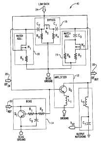
Fig. 1 is a circuit diagram of an exemplary low noise amplifier ("LNA") 10
according to
one embodiment of the claimed invention. The LNA 10 includes a bipolar
amplification circuit
12, a DC biasing network 14, a bypass switching network 16, and match
adjustment circuits 18,
19. In a preferred embodiment, all of the circuit elements shown in Fig. 1 are
located on a single
integrated circuit (IC). In addition, the LNA 10 may also include off-chip
circuit elements for
input and output impedance matching, which are described below with reference
to Fig. 2.
Operationally, the LNA 10 functions in two modes, a high-gain mode and a low-
gain
mode. While in high-gain mode, an RF input signal 20 is amplified by the
bipolar amplification
circuit 12 and DC biasing network 14 to generate an RF output signal 22. When
switched into
low-gain mode, the DC biasing network 14 is disabled, and the RF input signal
20 is fed forward
to the RF output 22 through the bypass switching network 16. In this manner,
power is
conserved when a high-power RF input signal 20 is received that does not
require amplification.
In addition, the match adjustment circuits 18, 19 are enabled in low-gain mode
in order to
compensate for input and output impedance differences between the bipolar
amplification circuit
12 and the bypass switching network 16.
The bipolar amplification circuit 12 is preferably a single-stage amplifier
that includes a
bipolar transistor QO and a degeneration inductor L1. The bipolar transistor
QO is preferably
sized to achieve high gain and a minimum noise figure. The degeneration
inductor L1 is
preferably coupled between ground and the emitter of QO in order to improve
the linearity of the
amplifier 12. The base of the bipolar transistor QO is coupled to the RF input
signal 20 and is
also coupled to the DC biasing network 14 to form a current mirror. The DC
biasing network 14
preferably includes a bipolar transistor Ql that is coupled to the bipolar
amplification circuit 12
3
CA 02361298 2001-11-07
through an RC circuit R1, R2, C0, and is also coupled to a DC reference
current (Iref) 23. The
DC reference current (Iref) 23 is preferably generated in a band gap reference
circuit configured
to provide a stable DC current that is substantially independent of
temperature and supply
voltage. The resistive values in the RC circuit R1, R2 control the amount of
current gain in the
current mirror, and thus determine the current of device Q0. The current
through device QO
defines its transit frequency, which together with L1 and the external
matching circuits define the
gain applied to the RF input signal 20 when the LNA 10 is in high-gain mode.
It should be
understood, however, that the biasing network 14 may be implemented using many
known
biasing circuits configured to form a current mirror with Q0, and is not
limited to the
implementation illustrated in Fig. 1. It should also be understood that
alternative embodiments
may include a minti-stage transistor amplifier, such as a cascode amplifier
configuration. The
use of a single-stage transistor amplifier, however, provides a low noise
figure and also
conserves power consumption by enabling low voltage operation.
The bypass switching network 16 includes an NMOS switch NO coupled between the
RF
input 20 and the RF output 22, and is controlled by a low-gain control signal
24. The bypass
switching network 16 also preferably includes two resistors R3, R4
respectively coupled between
ground and the drain and source terminals of the NMOS switch N0, and two
capacitors C1, C2
that block any DC components of the RF input and output signals 20, 22. These
resistive and
capacitive elements R3, R4, C1, C2 maintain a low DC voltage at the source and
drain of the
NMOS switch N0, thus improving the turn-on speed of the NMOS switch NO and
reducing the
impedance between the source and drain of NO when the switch NO is on.
The match adjustment circuit 18 preferably includes an input impedance
matching shunt
resistor RS coupled between ground and the RF input 20 through an NMOS switch
N1. The
4
CA 02361298 2001-11-07
NMOS switch N1 is controlled by the low-gain control signal 24, and couples
the impedance
matching resistor R5 to the RF input 20 when the LNA 10 is in low-gain mode.
The value of the
impedance matching resistor R5 is selected to maintain a substantially
constant input reflection
coefficient (S11) as the LNA 10 is switched from high-gain to low-gain mode by
compensating
for the impedance differences between the bipolar transistor QO and the NMOS
switch N0.
Preferably, the impedance-matching resistor combines with off-chip impedance
matching
components, discussed below with reference to Fig. 2, to match the input
impedance to a fifty
ohm (50SZ) source at the frequency band of interest. In addition, the
impedance matching
resistor R5 preferably compensates for parasitic impedance from the disabled
bipolar transistor
QO when the LNA 10 is in low-gain mode. In this manner, the off-chip impedance
matching
components may be selected to provide the desired input impedance (preferably
50SZ) when the
LNA 10 is in high-gain mode, taking into consideration the impedance of the
active bipolar
transistor Q0. Then, when the LNA 10 is switched to low-gain mode, the
impedance matching
resistor R5 is coupled to the RF input 20 to maintain a constant input
reflection coefficient (S11).
By compensating for the inherent impedance differences between bipolar and
NMOS devices
and the parasitic impedance of the bipolar transistor Q0, the input impedance
adjustment circuit
18 enables the use of a bipolar amplifier QO in the same LNA 10 as an NMOS
bypass switch N0,
thus combining the superior amplification properties of a bipolar transistor
with the superior
switching properties of an NMOS transistor.
Depending upon the operational frequency of the LNA 10, an additional match
adjustment circuit 19 may also be included at the output of the bypass
switching network 16 to
compensate for output impedance differences when the LNA 10 is in low-gain
mode. The output
impedance adjustment circuit 19 preferably includes an NMOS switch N2, two
resistors R6, R7,
5
CA 02361298 2001-11-07
and a capacitor C3. The NMOS switch N2 is controlled by the low-gain control
signal 24, and
couples the output impedance matching shunt resistor R7 in parallel with the
resistor R6 when
the LNA 10 is in low-gain mode. Similar to the input impedance adjustment
circuit 18, the value
of the impedance matching resistor R7 is chosen to compensate for the
impedance differences
between the NMOS switch NO and the bipolar transistor QO and parasitic
impedance from the
disabled bipolar transistor QO in low-gain mode. The impedance matching
resistor R7 preferably
combines with off-chip impedance matching components, discussed below with
reference to Fig.
2, to match the output impedance to a fifty ohm (SOS) load at the frequency
band of interest.
The resistor R6 and capacitor C3 are preferably included to improve the turn-
on performance and
reduce the impedance of the NMOS switch N2 by lowering the drain voltage of
the transistor
N2. Capacitor C3 serves to block any DC components. Resistor R6 maintains the
drain at OV
DC to ensure good switching of N2. Preferably, the value of impedance matching
resistor R7 is
small in comparison to the resistor R6 such that the value of R6 does not
significantly affect the
output impedance of the LNA 10.
Operationally, when the LNA 10 is in high-gain mode, the low-gain control
signal is
disabled, the NMOS switches N0, N1 and N2 are open, and the DC reference
current (Iref) 23 is
on, activating the DC biasing network 14. The DC reference current (Iref) 23
is amplified and
mirrored in the bipolar transistor Q0, thus amplifying the RF input signal 20
at the base of QO to
generate the RF output signal 22. When in high-gain mode, the bypass switching
network 16 has
little, if any, effect on the performance of the LNA 10. Then, when the low-
gain control signal
24 is enabled to enter low-gain mode, the NMOS switches N0, N1 and N2 are
closed, thus
activating the bypass switching network 16 and match adjustment circuits 18,
19. In low-gain
mode, the RF input signal 20 is fed forward through the bypass switching
network 16 to the RF
6
CA 02361298 2001-11-07
output 22, and the resistors R5, R7 are coupled to the circuit 10 to
compensate for input and
output impedance differences between the amplification circuit 12 and the
bypass switching
network 16. In addition, the DC biasing current (Iref) is preferably switched
off in low-gain
mode to conserve power.
Fig. 2 is a circuit diagram 30 of exemplary off-chip impedance matching
circuits 32, 34
for the LNA 10 shown in Fig. 1. The circuit 30 includes the LNA 10, an input
impedance
matching circuit 32 and an output impedance matching circuit 34. The input
impedance
matching circuit 32 preferably includes a series inductor L2 and a shunt
capacitor CS coupled
with the RF input 20. Capacitor C4 acts as a DC block. The output impedance
matching circuit
34 preferably includes an inductor LO coupled between the RF output signal 22
and a supply
voltage 36, a capacitor C7 coupled between the inductor LO and ground, and a
capacitor C6
coupled in series with the RF output 22. It should be understood, however,
that other known
impedance matching configurations may be utilized for the input and output
impedance matching
circuits 32, 34.
The values of the components in the input and output impedance matching
circuits 32, 34
are preferably chosen according to the operational frequency of the LNA 10 in
order to achieve
input and output matching, preferably to a fifty ohm (SOS2) source and load.
In addition, the
component values of the off-chip impedance matching circuits 32, 34 may be
varied in order to
adapt the LNA 10 shown in Fig. 1 to alternative near frequency bands. For
example, the values
of the off-chip impedance matching components L0, L2 and L6 shown in Fig. 2
may be varied to
switch the operational frequency band of the LNA 10 between the PCS band (1.96
GHz) and the
DCS band (1.84 GHz).
7
CA 02361298 2001-11-07
Fig. 3 is a circuit diagram of an exemplary LNA 40 having an on-chip output
impedance
matching inductor L0. Fig. 4 is a circuit diagram 50 of exemplary off-chip
impedance matching
components for the LNA 40 shown in Fig. 3. The LNA 40 shown in Figs. 3 and 4
is similar to
the LNA 10 described above with reference to Figs. 1 and 2, except that the
inductor LO and
capacitor C7 are included on the LNA integrated circuit. Placing these output
impedance
matching components L0, C7 on-chip results in a significantly more compact
design that is
particularly useful for applications, such as mobile communication devices, in
which circuit size
is a constraint. Fabricating the shunt inductor LO on the same silicon
substrate and in close
proximity to the degeneration inductor Ll, however, may cause significant
electromagnetic
coupling between the two on-chip inductors L0, Ll. Electromagnetic coupling
through the
silicon substrate and surroundings induces currents in the inductors L0, L1
thereby causing
feedback. Because the output impedance matching inductor LO is large with
respect to the
degeneration inductor L1, this feedback can cause excess current to build in
the degeneration
inductor L1, thereby destabilizing the amplifier 12. The two inductors L0, L1
thus act as a
transformer in which the magnetic field generated by current flowing through
the larger inductor
LO induces a current in the smaller inductor L1 and vice versa. To prevent
destabilization, the
inductors L0, L1 are preferably fabricated such that a negative feedback is
induced, i.e., the
induced current in the degeneration inductor Ll is in the opposite direction
of its operative
current flow. The polarities of the inductors LO,L1 are preferably selected to
ensure negative
feedback.
Fig. 5 is a schematic diagram 60 showing an exemplary fabrication layout of an
impedance matching shunt inductor LO and degeneration inductor L1 on a silicon
substrate. The
inductors L0, L1 may be fabricated on a silicon substrate using any known
integrated circuit
8
CA 02361298 2001-11-07
fabrication technique, and are preferably fabricated in an octagonal spiral
pattern as shown, but
may, alternatively, be fabricated in other patterns, such as a square or
circular spiral pattern. In
order to generate negative feedback between the inductors L0, L1, the spiral
patterns should
wind in opposite directions. For example, LO is shown with a counter-clockwise
winding
starting from the outside turn and L1 is shown with a clockwise winding. In
this manner, the
magnetic field of the impedance matching inductor LO will induce a negative
current flow (Iind)
62 in the degeneration inductor L1.
The inner termination point 67 of the impedance matching inductor LO is
preferably
coupled to the collector of the bipolar transistor QO shown in Fig. 3 and Fig.
5, and the outer
termination point 66 of the degeneration inductor L1 is preferably coupled to
the emitter of Q0.
Therefore, operational current flows into the inductors L0, L1 in the
direction shown by the
arrows in Fig. 5. The resultant magnetic field generated by the impedance
matching inductor LO
is illustrated by the circles 68, 70 at the center of the inductors L0, L1.
Using the right-hand rule,
one skilled in the art will recognize that the magnetic field generated by LO
flows out of the
plane of the paper at the circle 68 and reenters the plane of the paper at the
circle 70. This
magnetic field from LO thus induces a counter-clockwise current flow (Iind)
62, or negative
feedback, in the degeneration inductor Ll. Because the induced current (Iind)
is small in
comparison to the operational current (Iemitter) in the degeneration inductor
Ll, the negative
feedback does not significantly effect the operation of the LNA 40. If current
were induced in
the opposite direction, however, then the amplifier 12 could become unstable.
9
CA 02361298 2001-11-07
Multi-Band LNA
Preferably, the single-band LNAs described above with reference to Figs. 1-5
are
designed to function within a single RF frequency band. In order to create a
minti-band receiver,
two or more LNAs are preferably combined into one device, such as a dual-band
or triple-band
receiver. Each LNA in the minti-band receiver is preferably configured to meet
the requirements
of the frequency band of interest. For instance, in a mobile communication
device, a minti-band
receiver may include two or more LNAs configured to meet the frequency
requirements of
various cellular communication standards, such as GSM, EGSM, PCS and DCS.
Fig. 6 is a circuit diagram of an exemplary dual-band LNA 70 utilizing a
shared
degeneration inductor L3. The dual-band LNA 70 includes two single-band LNAs
72A, 72B and
the shared degeneration inductor L3. The single-band LNAs 72A, 72B are each
similar to the
exemplary LNA 10 described above with reference to Fig. 1, except the
amplification circuits
74A, 74B are both coupled to the single shared degeneration inductor L3. All
of the circuit
components shown in Fig. 6 are preferably included in a single integrated
circuit ("IC"). In
addition, off chip impedance matching circuits, as illustrated in Fig. 2, may
be coupled to the
input and output of each of the singe-band LNAs 72A, 72B.
The two single-band LNAs 72A, 72B are preferably configured to operate at near
frequency bands. For instance, one LNA 72A may be configured for the PCS band
(1.96 GI-Iz)
and the other LNA 72B for the DCS band (1.84 GHz). In this manner, a single
inductance value
L3 may be chosen that is suitable for both circuits 72A, 72B. When one LNA 72A
or 72B is
operational, the other LNA 72A or 72B is deactivated, and thus does not
significantly effect the
operation of the shared degeneration inductor L3. This function is possible
because a receiver
chain including the dual-band LNA 70 will operate at only one frequency band
at a given instant,
CA 02361298 2001-11-07
and, therefore, should never require the simultaneous use of both of the
single-band LNAs 72A,
72B. Thus, when one of the single-band LNAs 72A, 72B is in use, the other LNA
is preferably
powered down by setting its DC reference current (Iref) to zero. In
alternative embodiments,
additional components may be included to further isolate the inactive LNA 72A
or 72B from the
circuit 70. For instance, the base voltage of the bipolar transistors Q0, Q 1
in the amplification
circuit and DC biasing network of the inactive LNA 72A or 72B could be biased
or otherwise
clamped to a fixed voltage while the LNA is powered down. Furthermore, by
reverse biasing the
inactive transistor it's parasitic effects, such as parasitic capacitance, can
be further reduced.
The shared degeneration inductor L3 significantly reduces the amount of IC
surface area
required to fabricate a dual-band LNA 70. For example, the degeneration
inductor Ll in the
single-band LNA 10 shown in Fig. 1 may account for fifty percent of the space
required to
fabricate the circuit 10 on an IC. By utilizing a shared degeneration inductor
L3, a dual-band
LNA 70 can be fabricated that occupies only fifty percent more space than a
single-band LNA.
The embodiments described herein are examples of structures, systems or
methods
having elements corresponding to the elements of the invention recited in the
claims. This
written description may enable those skilled in the art to make and use
embodiments having
alternative elements that likewise correspond to the elements of the invention
recited in the
claims. The intended scope of the invention thus includes other structures,
systems or methods
that do not differ from the literal language of the claims, and further
includes other structures,
systems or methods with insubstantial differences from the literal language of
the claims.
11