Note: Descriptions are shown in the official language in which they were submitted.
CA 02361509 2001-10-22
High-Performance NxN Optical Matrix Switch Using Double-Size Butterfly
Network of 2x2 Switching Units
Technical Field
The present invention is an NxN optical waveguide matrix switch symmetrically
using
double-size butterfly network of 2x2 switch units. The 2x2 switch units are
preferred to
be Mach-Zehnder interferometer type because it has two advantages of low power
consumption and low access loss. It relates to a high-isolation, low
propagation loss, and
low-power-consumption optical switch for an optical communication system,
optical
interconnects, optical cross-connect, and a large-scale fiber-optic network
system.
Backsround of the Invention
Today, the rapid development and applications of fiber-optic telecommunication
systems are stimulating various photonics networks based on some new
microstructure
optoelectronic technologies instead of mechanical individual devices. Among
various
microstructure optoelectronic technologies, integrated optics represents a
promising
strategy in this field. One implementation of this strategy relies on the
integration of
optoelectronic interconnects on a host Si substrate, and thus requires
feasible
optoelectronic technologies in order to produce Si-based photonic devices. As
progress is
made on a variety of photonic networks, such as the optical cross-connects
(OXCs), the
dense wavelength division multiplexing (DWDM) and other kinds of optical
networks,
large-scale optical matrix switches are indispensable. These networks can
provide
flexible operations such as routing, restoration, and reconfiguration in the
DWDM
systems.
In long-haul transport networks, a hybrid technology is employed and traffic
is
transported optically, but most of operations are implemented as electronic
systems. The
switching and communication need to convert optical streams to electronic
signals and
then convert these signals to optical streams. The optical-electrical-optical
(0E0)
conversion based networks suffer from several inherent deficiencies such as
high cost,
lack of scalability and performance limitation. In local area networks,
optical switching is
an attractive candidate switching and communication. The optical matrix switch
is one of
most important components in constructing the photonic switching systems
including the
optical DWDM networks, the OXCs and multi-channel testing systems. The maximum
number of subscribers will strongly depend on the properties of the individual
matrix
switches. The requirements for the implementation of such matrix switches in a
system
are low loss and low crosstalk. Furthermore, the switch points of the devices
should have
uniform switch characteristics and stable operating characteristics. Today,
research and
development of optical matrix switches have had significant progress with
planar optical
waveguides and had some applications in fiber-optic communication systems.
They are
based on both the thermo-optic (TO) waveguides and the electro-optic (E0)
waveguides.
Typical contributions are made by the US Lynx Photonic Networks and the
Japan's NTT.
The TO matrix switch and the EO matrix switch are two promising candidates for
the
future photonic switching systems and the reconfigurable optical interconnects
of
switching systems. The former is generally based on silica-on-silicon
waveguides or
CA 02361509 2001-10-22
polymeric waveguides, while the latter is generally based on LiNb03 diffused
waveguides. For the large scale optical matrix switches, the silica-based
planar lightwave
circuits (PLC's) is the most promising technical approach because it has
lowest
propagation loss, reliable fabrication technique, easy mass-production,
polarization
insensitivity, and easy interfacing with fibers. The nodes of the optical
matrix switches
are the 2x2 switch units that can be either Mach-Zehnder interferometer-type
or digital-
optical switch. The TO waveguide devices using silica-on-silicon waveguides
have
shown an exciting advantage over the currently used mechanical and bulk optic
devices
in fiber-optic communications because of their great flexibility in
fabrication and
processing as well as speedy operations than the mechanical ones. The EO
waveguide
devices using diffused LiNb03-based waveguides have also presented a promising
application in the future with its high-speed operation, low loss and mature
manufacturing technology.
Most of optical switching devices in production today use an opto-mechanical
means
to implement optical steering. This is accomplished through the separation, or
the
alignment, or the reflection of the light beam by an opto-mechanical driven
mirror. These
designs offer good optical performance, but have some drawbacks. One is slow
speed.
The typical settling times for switching are from lOms to 100ms. Even for some
large-
scale optical matrix switches, the setting times for switching are from 100's
of
milliseconds to 1 second. The other disadvantage of the opto-mechanical
switches
includes the noise and size. These disadvantages could be acceptable in the
conventional
small-scale photonics networks, but today's high capacity communications
really could
not continue to suffer from these out-of age properties. To overcome some of
these
limitations, non-mechanical and no-moving-part optical matrix switch now
reaching the
market can use a variety of design concepts.
Totally there are two kinds of no-moving-part 2x2 optical waveguide switches:
one
uses the Mach-Zehnder interferometer (MZI) configuration and the other one is
digital
optical switch. 1 x2 and 2x2 switches are basic units for building the large-
scale matrix
switches and optical crossconnect (OXC) systems. The former has two
advantages: low
power consumption and low access loss, and a disadvantage: wavelength
sensitive. The
latter has two disadvantages: high power consumption and high access loss, and
an
advantage: wavelength insensitive. Thereby, the TOS using the MZI
configuration is
suitable for low thermal coefficient (dn/dT) and high reliability material
such as PECVD-
based silica-on-silicon and EOS using the MZI configuration currently uses the
LiNb03
diffused waveguides and will probably employ the reliable EO polymers in the
future.
Summary of the Invention
An NxN optical waveguide matrix switch using double-size butterfly network of
2x2
switching units is proposed in this invention. In the conventional NxN matrix
switches,
generally N to 2N switching stages and an NxN to 2NxN matrix of switching
units are
required to meet the optical signal communication between the input ports and
the output
ports. As a result, the device size, the complexity and the propagation loss
are headache
problems in the large-scale matrix switches. In this invention, the NxN
optical waveguide
matrix switch uses a double size butterfly network where the number of
switching stages
2
CA 02361509 2001-10-22
is logz + 2 , so not only can nonblocking degree and measurability be
increased, but also
both the number of 2x2 switching units and the number of switching operation
stages can
be decreased. More important is the number of switching operation stages is
significantly
reduced compared with what is used in the conventional optical matrix
switches.
Especially in the large-scale NxN matrix switches, this advantage becomes more
apparent. Thus, the propagation loss can be reduced to a much lower value than
the
conventional devices and the large-scale optical matrix switches can be built
in the same
size of wafers. Generally there are two kinds of 2x2 waveguide optical
switches: Mach-
Zehnder interferometer (MZI) switch and digital optical switch (DOS). The
former has
two main advantages: lower power consumption and lower access loss, and a main
disadvantage: wavelength sensitive. The latter has a main advantage:
wavelength
insensitive and two critic disadvantages: higher power consumption and higher
access
loss. The power consumption, the propagation loss and the wavelength
sensitivity are
three most important issues of a large-scale optical matrix switch based on an
accumulation of all the switching units and optical path that optical signals
pass through.
Therefore, the MZI type optical switch is preferred to use as a switching unit
because it
can directly meet two issues of the large-scale optical matrix switches with
its two main
advantages. Whereas, its disadvantage: wavelength sensitive can be solved by
another
way in this invention. If the wavelength sensitive 2x2 switching units such as
MZI type
optical switches are used as the switching units of the NxN optical waveguide
matrix
switch, at the different switching stages, the 2x2 switching units are
designed of different
central wavelengths to uniformly cover the whole wavelength range in this
invention. So,
the wavelength sensitivities among all the switching stages can be compensated
for one
another. Finally the performance of NxN optical matrix switch based on this
invention
becomes wavelength insensitive.
In a desirable embodiment according to the present invention, a 2N size full
butterfly
network is divided into two parts: one is used to perform an NxN switching
operation and
the other is used to have a high isolation outputs between any two adjacent
ports and test
output performance at off state. In addition, the two separate parts of
butterfly network
for switching operations and testing performance at the OFF-state can balance
the optical
paths and switching stages during it is performing the operations. In every
switching unit,
the MZI type switch is preferred and designed to work at different wavelengths
to
decrease the wavelength sensitivity of the whole NxN optical matrix switch
based on this
invention.
Brief Descriution of the Drawing
FIG. 1 is the configuration of an NxN optical matrix switch using the double-
size
mufti-stage butterfly network of 2x2 switch units: (a) the top view and the
construction of
the NxN optical matrix switch and (b) the cross-section view. This structure
comprises
two parts: the testing area of NxN and the switching area of NxN.
FIG. 2 is the configuration and operation principle of a 4x4 optical matrix
switch using
8x8 butterfly networks: (a) the complete construction, (b) the basic linking
principle, and
(c) an operation example.
FIG. 3 is the topology of 8-size butterfly network configuration: (a) the one-
stage
construction and (b) the three-stage construction.
CA 02361509 2001-10-22
FIG. 4 is the detailed structures of two kinds of Mach-Zehnder interferometer
type 2x2
switch as a switch unit or node of the butterfly network configuration: (a)
the normal
Mach-Zehnder interferometer and (b) the inverse Mach-Zehnder interferometer.
Detailed Description of the Invention
The matrix switches must be nonblocking, that means every input must have the
possibility to be interconnected to every output. In order to achieve this
point, a design of
matrix switch must meet a rearrangeable nonblocking network of permutation
nodes
involving the smallest possible number of switching units. Thus, a nonblocking
optical
matrix switch is a communication network between N input ports and N output
ports. In
fact, various communication networks have been studied and used for a long
time in the
conventional electrical communication systems. There are several popular
networks for
nonblocking communications of both electrical and optical networks such as
crossbar,
perfect shuffle, crossover, and butterfly. The crossbar network needs N
switching stages
for the nonblocking communication between N input ports and N output ports,
which
generally causes a higher propagation loss for the large-scale matrix
switches. The links
among the switching points, however, are simple and easy to be built with
optical
technique, so it is widely used in today's optical matrix switches. The latter
three kinds of
networks have a common advantage that they all only need logz + 1 switching
stages for
the nonblocking communications between N input ports and N output ports, but
they
have different structures of links among all the switching points, and these
three
structures of links have different complexities and difficulties in design and
fabrication in
optical devices. Among these three networks, the butterfly has been
demonstrated to have
the most regular links and is the easiest to be designed and fabricated in
both free-space
optical approaches and the PLCs. Especially, as described above, the PLCs
technique is
most promising in the fiber-optic communication systems.
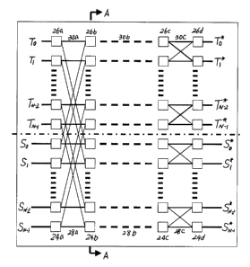
Figure 1 is the NxN optical waveguide matrix switch built with a double-size
butterfly
network where Fig. 1 (a) is the top view and Fig. 1 (b) the cross-section
view. This NxN
optical matrix switch comprises a substrate 20, cladding 22, active switching
units 24a,
24b, 24c and 24d, passive switching units 26a, 26b, 26c and 26d, waveguide
links 28a,
28b and 28c for the active switching units, waveguide links 30a, 30b and 30c
for the
passive switching units, electrodes 32a, 32b, 32c and 32d deposited on the
active
switching units and electrodes 34a, 34b, 34c and 34d for the passive switching
units. As
shown in Fig. 1 (a), the butterfly structure of the NxN optical matrix switch
based on this
invention is divided into two areas: one is used to implement the switching
operations
with external controls and called switching operation area and the other one
is used to test
optical performance at the OFF-state and balance the optical paths for the
optical signals.
The active switching units 24a through 24d are used for the switching
operations area, so
the electrodes 32a through 32d are required. The passive switching units 26a
through 26d
are used to pass through optical signals at the OFF-state, so the electrodes
34a through
34d are not required or optional. In the switching operations area, the input
ports at the
input end are labeled as So , S, , through SN_, , and the output ports at the
output end are
labeled as So , S; , through SN_, . In the testing area, the input ports at
the input end are
labeled as To , T, , through TN_, , and the output ports at the output end are
labeled as To ,
CA 02361509 2001-10-22
T,' , through TN_, . In fact, the switching operations area and the testing
area are
symmetric with each other if the electrodes are deposited for both the
switching
operations area and the testing area. So, these two areas are equivalent to
each other. In
other words, the switching operations area can be used as the testing area and
the testing
area used as the switching operations area. From the viewpoint of functions,
the
switching operations area is core part of the optical matrix switch based on
this invention.
Namely, in the switching operations area, each switching unit has to have two
switching
options for any input optical signal, so the modulating electrodes 32a through
32d are
necessary for each unit to implement the switching operations. Whereas, the
testing area
is used for testing the isolation and uniformity among all the output ports at
the OFF-state
of the whole system and balancing the optical paths among all the optical
links during the
optical switching units are operating. Namely, in the testing area, each
switching unit
does not have to have two switching options, but one operation state at the
OFF-state. So,
once the testing area is specialized, all the electrodes 34a through 34d for
the passive
switching units can be ignored, but the optical structure used in each
switching unit
should be the same as the counterpart of the switching operations area. Figure
2
illustrates an NxN optical matrix switch using a double-size butterfly network
as depicted
in this invention when N=4. In other words, a 4x4 optical matrix switch using
an 8x8
butterfly network. Figure 2(a) shows the complete link construction of the 4x4
optical
matrix using 8x8 butterfly network based on this invention. The input ports of
the
switching operations area are So , S, , SZ and S3 , and the output ports of
the switching
operations area are So , S; , Sz and S3 . In the same manner, the input ports
of the testing
area are To , T, , TZ and T3 , and the output ports of the testing area are To
, T' , Tz and T3 .
The four columns of switching units 24a, 24b, 24c and 24d in the switching
operations
area and the four columns of switching units 26a, 26b, 26c and 26d in the
testing area are
connected into a 8x8 butterfly network by the three-stages of links 28a, 28b
and 28c in
the switching operations area and the three stages of links 30a, 30b and 30c
in the testing
area. Figure 2(b) illustrates the operating principle of the 4x4 optical
matrix switch using
8x8 butterfly network based on this invention. In the practical operations for
all the
optical signals: 36a, 36b, 36c and 36d, not can all the links be used. Only
some of them
can be used like the solid lines of Fig. 2(b) and some of them can never be
used and are
always at the idle state like the dashed lines of Fig. 2(b). If the four
optical signals 36a,
36b, 36c and 36d are launched into four input ports: So , Sl , SZ and S3 ,
respectively,
they have to pass through the first column 24a of switching units of the
switching area
first at the OFF-state of the switching units 24a, i.e., no modulating effects
are applied
onto these switching units. Then, these four optical signals: 36a, 36b, 36c
and 36d will be
butterfly connected to the second column 26b of the switching units of the
testing area by
the linking stage 28a. Forward butterfly connections to the successive stages
30b and 30c
of links are performed only in the testing area and the OFF-state switching
operations in
the testing area are performed by the second column 26b, the third column 26c
and the
fourth column 26d of the switching units, respectively. Finally, as shown in
Fig. 2(b),
these four optical signals are output in the inverse order of the input. Thus,
all the straight
links (the dashed lines) of the testing area cannot be used and only the
butterfly links (the
solid lines) are used. Even the first column 26a of the switching units of the
testing area
and the first stage 30a of all the links from these switching units are always
in the idle
CA 02361509 2001-10-22
state. Note that all the optical signals must be coming out from the output
ports of the
testing area if no modulating effect applied onto the switching units of the
switching area,
so any linking path of an optical signal from one input port to one output
port of the
switching operations area must be based on the modulating effect applied onto
the
switching units for switching operations. For example, as shown in Fig. 2(c),
if the
switching units having hatched lines indicate the modulated state, i.e., the
first switching
unit from top of units 24a, the first switching unit from top of units 24b,
the third
switching unit from top of units 24c and the third switching unit from top of
units 24d,
the optical signal 36a launched into the input port So of this 4x4 optical
matrix switch
will be coming out at the output port Sz . As depicted in Fig. 2(c), the
operating process
has been marked with the bigger lines. The same optical signal 36a can also
have other
output choices by modulating different group of switching units, so one
optical signal can
choose any one among the four output ports. In the same manner, all other
optical
signals: 366, 36c and 36d have the same four output choices as the optical
signal 36a.
Even an NxN optical matrix switch can be constructed in this style. Therefore,
an NxN
optical matrix switch can be implemented based on the operation principle
defined by
this invention.
The waveguide switch based on the Mach-Zehnder interferometer (MZI)
configuration
contains two 3d8 directional couplers connected by two waveguide arms. This
kind of
switches basically exploits the phase property of the light. The input light
is split and sent
to two separate waveguide arms by the first 3dB directional coupler, then
combined and
split one last time by the second 3dB directional coupler. One or two of the
waveguide
arms are modulated to produce a difference of optical path length between
these two
waveguide arms. The modulating means can be either thermo-optic (TO) or
electro-optic
(E0). If these two optical paths are the same length, light chooses one exit,
if they are
different it chooses the other. As a 2x2 switch, for one input optical signal,
the isolation
between two output ports is important because it directly determines the
isolation
between two output ports for the same input optical signal. The isolation is
strongly
dependent of the coupling ratio of the two 3dB directional couplers. Namely,
the closer to
50% the coupling ratio of the 3dB directional coupler is, the higher the
isolation of the
2x2 switch is, and further more the higher the ON/OFF extinction ratio of each
output
port is. In theory, if the coupling ratio of the 3dB coupler is exactly 50%
(i.e., -3dB), the
isolation between two output ports should be infinity. In fact, no perfect 3dB
directional
coupler exists because the errors in both design and fabrication, especially
in fabrication,
are not avoidable. So, a real isolation of around 20 dB is not easy for any
2x2 waveguide
switch having an MZI configuration to be achieved. In the real fiber-optic
communications, not only isolation of more than 20 dB is popularly required
for the
protection switching systems, but also is the isolation of more than 30 dB,
even more
than 40 dB is always and strictly required for some more important DWDM
networks
such as typical optical add/drop multiplexing systems. Fortunately, the NxN
matrix
switches generally have several stages of MZI operations, so the isolation is
easy to meet.
The butterfly network has a size of N = 2" where N indicates the network size
(the
port number) and n the number of linking stages. The butterfly network is
suitable for
various multistage networks (MN) in which the link interconnection patterns
often
CA 02361509 2001-10-22
include sizes N , N l 2 , N l 4 , etc. The perfect shuffle, the crossover, and
the butterfly
networks are topologically equivalent because each node has two fan-in and two
fan-out
lines. For a one-stage butterfly network, as shown in Fig. 3(a), with two fan-
in lines or
two fan-out lines at each node, one is a straight interconnect line and the
other is a
butterfly interconnect line. We define the address numbers of the nodes with
straight lines
and butterfly interconnect lines as KS , and Kb ( Ks, Kb = 0,1,..., N -1) ,
respectively, on
the output end and as k on the input end. For the butterfly network, we have
the
following relations:
Ks = k (k = 0,1,..., N -1) ( 1 )
_ k+Nl2 (k < Nl2)
Kb k-Nl2 (N/2 <_ k < N) (2)
To analyze and compare the construction features of the butterfly network, let
us define
8 = K~ - k , which represents the interconnect angles of link lines from the
input end to
the output end. Then, we have, from Eqs. (1) and (2),
85 = Ks - k = 0 (k = 0,1,..., N -1) (3)
N l 2 (k < N l 2) (4)
Sb =Kn-k=
-Nl2 (N/2 <- k < N)
Note from Eqs. (3) and (4) that not only the interconnect angles of the
straight
interconnect lines ( 8S ) but also those of the butterfly interconnect lines (
8b ) are
independent of the number of address nodes k ; that is, not only all the
straight
interconnect lines but also the butterfly interconnect lines are parallel,
which is also easy
to see in Fig. 3(a). In other words, the butterfly networks have more
architectural
advantages, which is important for the implementation of the PLCs.
As mentioned above, the normal butterfly network has the same advantages as
other
two networks: perfect shuffle and crossover. The first is that loge + 1
operation stages are
needed for an N port network. The second is that there is a connection line
between any
port at input end and any port at output end. A normal butterfly network with
N=8 is
shown in Fig. 3(b). Then we have the following mathematical relation to
describe the
topology of this network. The topology of a multistage network is defined by
three
physical parameters: (1) the type of switching element comprising a node, (2)
the number
of node stages, and (3) the link interconnections provided between adjacent
node stages.
Both fully connected data butterfly networks with N nodes require loge + 1
node stages,
in which each node stage is labeled in sequence from 0 to loge . The input
(leftmost)
node stage is assigned label 0 , and the output (rightmost) node stage is
assigned label
logz . Each switching unit (node) in a particular node stage is assigned a
unique physical
7
CA 02361509 2001-10-22
address with an address bit (K;_" K;_Z,..., Ko) , where i = loge . The
physical address
identifies the unit's relative location within the node stage, with the top
node labeled as 0
and the bottom node labeled as N -1.
In the butterfly networks a pair of interconnections provided by the links
within link
stage i can be mapped as B° and B;' . These points represent the
straightforward
connection and the butterfly connection, respectively, and they map a node
(K;_,,...,K;,...,Ko); in node stage i two nodes in node stage i+1. The
relationships
between the node in node stage i and the two nodes in node stage i + 1 are
described by
B,,°(K;_,K;_Z,...,K,_;+,,...,Ko) _
(K;K;_,,...,K,_;+I,...,...,0,...,K,_;_,,...,K,);+,
for link (K;_,,K;_Z,...,K,);+, , 0 5 i < 1, (5)
B; (K;_,K;_z,...,K,_;+,,...,Ko) _
(K;K;_,,...,K,_;+,,...,...,1,...,K,_;_,,...,K,);+,
for link (K;_,, K;_z,..., K, ).+, , 0 <_ i < 1, (6)
Then for the (i + 1)th stage the link relationship of K;+, is shown by
K° , = K; , K; = 0,1,..., N -1, 0 <_ i < 1, (7)
K; +Nl2',[(j-1)Nl2' < K;+, <_ jNl2']
K'+' = K~ _ ~r/2'~~jNl2' <_ K,+, < jNl2'~
j =1,2,...,2') . (8)
As mentioned above, every node of the butterfly network has two fan-in lines
and two
fan-out lines at all the operating stages, and every node of input end has one
fan-in line
and two fan-out lines, and every node of output end has two fan-in lines and
one fan-out
line. Each node indicates a switching unit and needs a 2x2 or 1 x2 switch to
perform its
options of links. As well known, totally there are two kinds of 2x2 optical
waveguide
switches: the MZI type and the DOS. The former has two main advantages: lower
power
consumption and lower access loss, and a main disadvantage: wavelength
sensitive. The
latter has a main advantage: wavelength insensitive and two main
disadvantages: higher
power consumption and higher access loss. The power consumption, the
propagation loss
and the wavelength sensitivity are three most important issues of a large-
scale optical
matrix switch based on an accumulation of all the switching units and the
optical paths
that optical signals pass through. Thus, the MZI type optical switch is
preferred to use as
a switching unit because it can directly meet two issues of the large scale
optical matrix
switches with its two main advantages and its disadvantage: wavelength
sensitive can be
solved by another way in this invention. If the wavelength sensitive 2x2
switching units
such as MZI type optical switches are used as the switching units of the NxN
optical
waveguide matrix switch, at the different switching stages, the 2x2 switching
units are
designed for different central wavelengths to uniformly cover the whole
wavelength
g
CA 02361509 2001-10-22
range. So, the wavelength sensitivities among all the switching stages can be
compensated for one another. Finally the performance of NxN optical matrix
switch
based on this invention becomes wavelength insensitive. In addition, in order
to balance
the switching operations at different switching stages, two kinds of MZI
switches: the
normal type and the inverse type are suggested to alternatively use.
Figure 4(a) and Figure 4(b) show two types of MZI type switches: the normal
type and
the inverse type. As shown in Fig. 4(a), the normal MZI unit is composed of
two 3dB
directional couplers 38a and 38b connected by two waveguide arms. One heater
40
deposited on one of two arms, which is used to modulate the optical path of
MZI unit. In
this MZI unit, two waveguide arms have the equal length, so it is called
normal MZI
configuration. Two input ports are labeled as 42a and 42b, and two output
ports as 44a
and 44b. If an optical signal 46a is launched into the input port 42a, it is
split into two
parts at 50% coupling ratio by the first 3d8 directional coupler 38a, then
these two parts
are combined into one optical signal again by the second 3dB directional
coupler 38b. If
the heater (or electrode) 40 is not activated (at the OFF-state), this
combined optical
signal is sent to the output port 44b by the second 3d8 directional coupler.
This coupling
process at the OFF-state is the same as one 100% directional coupler because
these two
waveguide arms have an equal optical length and no extra optical phase change
is
induced. So, this type of MZI is called normal configuration. If the heater
(or electrode)
40 is activated by electrical power (or electric field) to produce an optical
phase change
of ~c (at the ON-state), this optical signal 46a is sent to the output port
44a. In the same
manner, if an optical signal 46b is launched into input port 42b, it will come
out at the
output port 44a at the OFF-state and will come out at the output port 44b at
the ON-state.
In an inverse MZI configuration, as shown in Fig. 4(b), between two 3dB
directional
couplers 48a and 48b, two waveguide arms have phase difference of ~. So, this
type of
MZI is called as inverse MZI configuration. A heater (or electrode) 50 is
deposited on
one of two waveguide arms. Two input ports are labeled as 52a and 52b, and two
output
ports as 54a and 54b. If an optical signal 56a is launched into the input port
52a, it is split
into two parts at 50% coupling ratio by the first 3dB directional coupler 48a
and then
these two parts are combined into one optical signal again by the second 3d8
directional
coupler 48b. If the heater (or electrode) 50 is not activated (at the OFF-
state), there has
been an optical phase difference of ~ between two waveguide arms, so the
combined
optical signal is sent to output port 54a. This coupling process is exactly
the inverse to
one 100% directional coupler, so it is called inverse MZI configuration. If
the heater (or
electrode) 50 is activated by electrical power (or electric field) to produce
an extra optical
phase change of ~ (at the ON-state), this combined optical signal 56a is sent
the output
port 54b by the second 3dB directional coupler 486. In the same manner, if an
optical
signal 56b is launched into input port 52b, it will come out at the output
port 54b at the
OFF-state and will come out at the output port 54a at the ON-state.
Finally two useful papers for understanding the topology of "butterfly
network" are the
following:
9
CA 02361509 2001-10-22
~ Butterfly interconnection implementation for n-bit parallel full-adder and
subtracter by Sun, et al., Optical Engineering, Vol. 31, No. 7, July 1992, pp.
1568-
1575;
~ Butterfly interconnection networks and their applications in information
processing and optical computing: application in fast Fourier transform-based
optical information processing by Sun, et al., Applied Optics, Vol. 32, No.
35,
December 1993, pp. 7184-7193.