Note: Descriptions are shown in the official language in which they were submitted.
CA 02362029 2001-08-17
WO 00/49782 PCT/US00/04062
1
A SYSTEM AND METHOD FOR RECOVERING SYMBOL TIMING
OFFSET AND CARRIER FREQUENCY ERROR IN AN OFDM DIGITAL
AUDIO BROADCAST SYSTEM
BACKGROUND OF THE INVENTION
FIELD OF THE INVENTION
The present invention relates to the field of digital communications, and more
specifically, is directed to a system for acquiring or recovering a symbol
timing offset and
carrier frequency error from a digitally modulated, mufti-carrier
communications signal. The
system of the present invention is further directed to a diversity system for
recovering a
symbol timing offset and earner frequency error from a diverse, mufti-
frequency digitally
modulated signal.
PRT(1R ART
to In a digital communication system, the acquisition of symbol
synchronization
between the transmitter and receiver must be achieved before effective symbol
demodulation
can commence at the receiver. Thus, the prior art in digital communications is
replete with
attempts to develop systems directed to the optimal recovery or acquisition of
received
symbol timing and carrier frequency.
One such attempt is provided in U.S. Patent #5,541,552, by Suzuki, directed to
the
demodulation of digitally modulated mufti-carrier symbols. The receiver in
this Patent
develops correlation peaks responsive to an intra-symbol correlation, as by
conjugate product
formation, between the repetitive information and the amplitude tapering
existing at the
leading and lagging portions of each received symbol. The peaks must be
detected, for their
2o positions are indicative of received symbol timing. However, their
relatively flat amplitude
profiles necessitate their individual integration prior to the peak detection
thereof.
This simplistic signal processing scheme in Suzuki, i.e., mere integration of
correlation peaks prior to their detection, provides sub-optimal
synchronization results on at
least two accounts. First, as the number of frequency carriers is increased in
the mufti-earner
symbol, the correlation peak becomes obscured by adjacent noise, and mere
integration fails
to sufficiently enhance the signal-to-noise ratio of the pre-detected
correlation peaks. Second,
mere integration fails to combat well known signal propagation effects, such
as scattering,
CA 02362029 2001-08-17
12-04-2001 , US 000004062
0..,_~ ____,_x:45 FAa 412 5BB 8089 ECHERT SEAMANS
2
fading, or other signal interferers, all of which combine to cause signal drop-
outs and false
peaks.
- Mochizuld, N. et al., "A 1-Iigh Perfr~rmance Fre9uency anrl Timing
Synchronization
Technique for OFDM", IFFR Global Telecommunications Conference, U.S., New
York,
New York, TEES 1998, P. 3443-3448, discloses a signal-repetition based
frequency and
timing synchronization technuique for burst Ol~DM moderns in sever fading
environments.
In contrast to SuzulQ and other prior art acquisition systems, the system of
.the
present intvention presents an optimum scheme for the recovery of symbol
timing and
carrier frequency_ This optimum approach is provided through an application of
signal
processing techniques that, when taken eitb~er alone or in combination,
improve over the
prior art. These signal processing inctprovements include the additive
superposition of
repeating signals, optimum or matched filtering, and diversity selection and .
combining
between diverse, modulated signals.
Published Patetzt Application '0lrQ A 97 49207 discloses a digital aadio
broadcasting
system in which pluralities of digitally modulated sub-carriers are
transmitted in upper and
lower sidebands simultaneously with an analog modulated carrier in a comumon
radio
channel. However, published Patent Application WO A 97 49207 does not disclose
a
technique for determining ~syrnbol timing offset and synchronization at
receivers in digital
audio broadcasting systems.
The following is a list of prior art references known to Applicant: L1.S.
Patents
#5,694,389; #5,62,835; #5,608,764; #5,559,833; #5,687,165; #5,541,552;
#5,357,502;
#3,925,650; #5,596,582; #3,364,482; #2,943,316; #3,975,687; #5,594,761;
#4,281,412;
#5,187,711; #4,727,534; #5,369,$00; #5,548,819; #2,549,423; #2,880,275;
#3,555,427;
#5,629,639; #5,428,647; #5,682,376; #5,416,767; #5,452,331; #4,344,180;
#S,6S7,313;
#5,652,772; #5,627,863; #5,550,812; #5,506,836; #5,471,464; #5,450,456;
#5,371,761;
#5,345,440; #5,313,169; #5,228,025; #5,191,576; #5,371,54$; #5,406,551; and,
#3,78(1,279_
~~Ml~~l~.~TH~ INV7=~1T~,01't
1t is an object of the present invention to provide a system for optimally
recovering symbol
timing and carrier frequency from a digitally modulated, multi-carrier signal.
AMENDED SHEET
CA 02362029 2001-08-17
12-04-2001 US 000004062
, _. __. _ _ . _; _5: 4S FAa 412 s88 8099 ECRERT SF.A3iANS _ _
3
Particularly, the digitally modulated signal is an orthogonal frequency
division multiplexed
(OFDM) sigaal that can include a large number of carriers therein.
One aspect of the present invention presents a system for recovering a symbol
timing
offset and carrier JSrequency error from an OFDM signal. The system includes a
receiver
module for receiving t3ye OFDM modulated signal which is represented as a
series of OPDM
symbols. Each OFDM symbol includes a leading portion aad a trailing portion
thereof. The
leading aad trailing portions have substantially equivalent phases and have
temporally
weighted amplitudes according to a prsdetc~mined temporal weighting function.
The
receiver module provides a received signal to an output thereof.
The system also includes a signal peak development module which develops a
boundary signal having a plurality of signal peaks representing a symbol
boundary position
for each of the received OFDM symbols. Each of the signal peaks is developed
responsive
to an ampFitude and phase correspondence produced between the leading and
trailing
portions of the received OFDM symbol.
The system further includes a signal enhancing module that enhances signal
peak
detectabiIity of the boundaxy signal. The signal enhancing ~»odule includes a
circuit for
additively superimposing a plurality of segments of the boundary signal. The
signal
enhancing module outputs an enhanced signal peak corresponding to a
predetermined
munber of the plurality of segments and having an improved signal to-noise
ratio.
The system includes a circuit, for establishing a temporal position indicative
of the
symbol boundary position from at least one of the enhanced signal peaks output
from the
signal enhancing module. The temporal position represents a received OFDM
symbol
timing offset.
A circuit for recovering the received OFDM signal carrier frequency error in
correspondence with said temporal position is also included in the system.
1~he signal enhancing module further iacludes a matched filter for filtering
signals
produced responsive to the boundary signal. The matched fitter further
improves a signal-
to-noise ratio of the enhanced signal peaks output from the
AMENDED SHEET
CA 02362029 2001-08-17
0 12_04-2001 J:45 FAg 412 588 8099 ECxERT SEAMANS US 000004062
3a
signal enhancing u~odulc. The matched filter has a tcanporal impulse response
matched to
the amplitude envelope of the signal peaks present in the boundary signal.
Anotizer object of the present invemion is the improvement of the symbol
timing and
frequency carrier acquisition process through the application of signal
diversity selection
S and combining. to the diversity aspect of the present invention, a diversity
system for
recovering a symbol tinning offset and carrier frequency e~exor from the OFDM
signal
includes a transmitter far transmitting an OFDM modulated signal in both
AMENDED SHEET
CA 02362029 2001-08-17
WO 00/49782 PCT/US00/04062
4
an upper and a lower frequency sideband. Each of the sidebands encompass a
plurality
of OFDM modulated frequency carriers and a series of OFDM symbols.
The diversity system includes a receiver portion for receiving the OFDM
modulated signal of the upper frequency sideband and providing a first or
upper
sideband received signal output and the OFDM modulated signal of the lower
frequency
sideband and provides a second or lower sideband received signal output.
The diversity system also includes a first recovery circuit for developing a
first
or upper sideband symbol timing offset corresponding to OFDM symbols in the
first
received signal, and a second recovery circuit for developing a second or
lower sideband
to symbol timing offset corresponding to OFDM symbols in the second received
signal.
Further, the diversity system includes a first validation circuit for
validating the
first symbol timing offset based on a predetermined temporal consistency
thereof, and a
second validating circuit validating said second symbol timing offset based on
a
predetermined temporal consistency thereof.
Still further, the diversity system includes a selection circuit for selecting
an
optimum symbol timing offset from the first and second symbol timing offsets
responsive to signals output from the first and second validating circuits,
and a
demodulator circuit for demodulating at least one of the series of OFDM
symbols using
the optimum symbol timing offset.
2o A further aspect of the diversity system includes a circuit for developing
a third
or combined symbol timing offset corresponding to a combination of first and
second
timing signals respectively representative of the first and second symbol
timing offsets,
and a circuit for selecting the third symbol timing offset responsive to a
plurality of
conditional input signals.
BRIEF DESCRIPTION OF THE DRAWINGS
FIG. 1 a is a graphical representation of the OFDM signal in the frequency
domain;
FIG. lb is a graphical representation of the OFDM signal in the time domain;
FIG. 1 c is a graphical representation of the conjugate product signal peaks
3o representing symbol boundaries;
CA 02362029 2001-08-17
WO 00/49782 PCT/US00/04062
FIG. ld is a graphical illustration of the conjugate products multiplied by
respective amplitude tapers;
FIG. 2 is a partial block diagram illustrating the front end portion of the
present
invention;
5 FIG. 3 is a block diagram of a first embodiment of the acquisition module of
the
present invention;
FIG. 4 is a block diagram of a second embodiment of the acquisition module of
the present invention;
FIG. 5 is a block diagram of a third embodiment of the acquisition module of
the
1 o present invention;
FIGS. 6a, 6b and 6c are graphical representations of symbol timing for the
peak
development module of the present invention;
FIGS. 7a, 7b, 7c and 7d are graphical representations illustrating the signal
processing performed by the present invention; and,
FIG. 8 is a block diagram representing the decisional and selection logic
blocks
for the diversity combining logic module of the third embodiment (FIG. 5) of
the
present invention.
DESCRIPTION OF THE PREFERRED EMBODIMENTS
In a digital communication transmission-reception scheme wherein a series of
digitally modulated information carrying signals are transmitted to a receiver
whereat
demodulation of the symbols is to occur in order to recover the information
conveyed
thereby, the receiver demodulator can achieve successful and optimum
demodulation of
the symbols only if the transmitted symbol timing and phase/frequency are
ascertainable
at the receiver. Thus, prior to such successful demodulation of the received
symbols,
the receiver must acquire or recover the received symbol timing and carrier
phase/frequency, both of which are to be utilized by the demodulation process.
Once
received symbol timing and frequency have been recovered at the receiver and
thereafter
the demodulation of the symbol has begun, symbol timing and carrier frequency
can be
tracked by way of a servoloop in order to maintain the integrity of the
demodulation
3o process. The system or architecture in the present invention is directed to
the
CA 02362029 2001-08-17
WO 00/49782 PCT/US00/04062
6
transmission of a series of digitally modulated symbols to a receiver whereat
demodulation of the symbols is to occur. More particularly, the system in the
present
invention is directed to the acquisition of received symbol timing offset and
carrier
phase/frequency error so that effective demodulation and subsequent tracking
of symbol
timing and carrier frequency can commence.
The system and method for acquiring or recovering symbol timing offset and
frequency error in the present invention is particularly well suited to an
environment
wherein the transmitter transmits and the receiver receives an orthogonal
frequency
division multiplexed (OFDM) signal. Referring to Fig. la, the OFDM signal used
in the
1 o present invention is characterized as a mufti-frequency Garner signal
comprising the
plurality of equidistantly spaced sub-carriers fl-fn. Adjacent sub-carriers,
such as fl
and f2, are separated each from the other by a predetermined frequency
increment such
that adjacent sub-Garners are orthogonal, each to the other. By orthogonal, it
is meant
that when properly Nyquist weighted, the subcarners exhibit no crosstalk. In
one hybrid
system incorporating the instant invention and using both digital and analog
transmission channels, there are 191 Garners in each sideband with a 70 kHz
bandwidth
for each sideband. In one all digital implementation of the instant invention
there are
267 Garners in each sideband with a 97 kHz bandwidth for each sideband.
Referring to Fig. lb, in the time domain, each OFDM symbol 5 has an effective
2o symbol period or temporal width T, and a full symbol period Ta . The OFDM
subcarrier
orthogonality requirement creates a functional interdependency between the
effective
symbol period T and the frequency spacing between adjacent OFDM subcarners.
Specifically, the frequency separation between adjacent subcarriers is
constrained to be
equivalent to the inverse of the effective symbol period T of each OFDM symbol
5.
That is, the frequency separation is equal to 1/T.
Turning again to Fig. 1 b, extending across the effective symbol period T of
each
OFDM symbol 5 are a predetermined number N of equidistantly spaced temporal
symbol samples (not shown in the Figure). Further, extending across the full
period Ta
of each OFDM symbol 5 are a predetermined number N« = N(1+a.) of equidistantly
3o spaced temporal symbol samples. As will be described subsequently in this
disclosure,
CA 02362029 2001-08-17
WO 00/49782 PCT/US00/04062
7
oc is the amplitude tapering factor for the symbol, and can be considered here
as a
fractional multiplier. Even further, predetermined amplitude-time profile or
envelope
10,15,20 is imposed upon the signal levels of these samples. This amplitude
profile
includes symmetrically ascending and descending amplitude tapers 10,15 at the
leading
s portion and trailing portion of each symbol 5, respectively, and a
relatively flat
amplitude profile 20 extending therebetween. These rounded or tapered edges
provided
in the time domain serve to substantially reduce undesirable side-lobe energy
in the
frequency domain, to thus provide a more spectrally efficient OFDM signal.
Although
the full symbol period Ta of symbol 5 extends beyond the effective symbol
period T,
to orthogonality between adjacent sub-carriers in the frequency domain (Fig.
la) is not
compromised so long as amplitude tapers 10,15 of symbol 5 follow a Nyquist or
raised-
cosine tapering function. More specifically, orthogonality is maintained in
the present
invention through a combination of root-raised cosine weighting (or amplitude
tapering)
of transmitted symbols and root-raised cosine matched filtering of received
symbols.
i s The leading and trailing portions of OFDM symbol 5 share an additional
important feature, namely, the first N OFDM symbol samples extending across
the
leading portion of OFDM symbol 5, which has a temporal duration aT, have
substantially equivalent phases as the last a.N symbol samples extending
across the
trailing portion of OFDM symbol 5, which also has a temporal duration a.T.
Note again
2o that a, is the amplitude tapering factor for the symbol, and can be
considered here as a
fractional multiplier. As will be described more fully herein, these
predetermined
amplitude and phase properties inherent in the leading and trailing portions
of the
OFDM symbol of the present invention, namely, the tapering of sample
amplitudes in
the leading and trailing portions of each OFDM symbol and the equivalent
phases
25 thereof, are advantageously exploited in the system of the subject
invention in order to
efficiently acquire OFDM symbol timing and frequency in the receiver, so that
the
demodulation of the symbol can commence.
Having described the characteristics of the OFDM symbol used in the the
present invention, the system for recovering system timing in the present
invention is
3o now described. Referring to Fig. 2, the digital communication transmission-
reception
CA 02362029 2001-08-17
WO 00/49782 PCT/US00/04062
8
system of the present invention includes an OFDM modulator module 25 for
generating
OFDM modulated transmit signal 30 at an output thereof, which is transmitted
to
OFDM signal receiver 150 for demodulation thereat by OFDM demodulator 100.
OFDM transmit signal 30 generated by OFDM modulator 25 conforms to the OFDM
signal specifications shown in Figs. 1 a and 1 b and described previously.
That is,
OFDM modulator 25 generates a series of OFDM symbols 5, as shown in Fig. lb,
each
of which comprises a predetermined number of temporal symbol samples Na
corresponding to full symbol period Ta, wherein the first aN samples and the
last aN
samples of each symbol are tapered and have equal phases. To facilitate
further
1 o discussion of symbol signal processing, it will be assumed that the
predetermined
number Na of temporal samples extending across each full symbol period Ta is
1080,
that the predetermined number N of temporal samples extending across each
effective
symbol period T is 1024, and that the number of samples in each of the first
aN samples
and last aN samples is 56, however, these values are merely exemplary and may
be
varied in accordance with system requirements. Note further that information
source 40
provides information signals to an input of OFDM modulator 35, which
information
signals are modulated onto OFDM symbols in signal 30.
OFDM transmit signal 30 is transmitted to OFDM signal receiver 150 by any
mechanism and through any medium known in prior art communication systems. For
2o example, OFDM transmit signal 30 can be provided as an analog signal, a
radio
frequency signal such as an audio broadcast signal, or alternatively, can be
provided
even as a digital base band signal. The physical mediums 45 through which
signal 30 is
transmitted can be atmospheric, optical, wireline, or otherwise.
Alternatively, transmit
signal 30 can be a computer generated signal suitable for simulation purposes,
that is, a
computer generated signal that is communicated between software program
modules, as
between a computer program based OFDM modulator module, and a computer program
based OFDM signal receiver module. None of the foregoing variations affect the
advantageous application of the system architecture and techniques of the
present
invention to provide OFDM symbol timing offset and frequency error
acquisition.
CA 02362029 2001-08-17
WO 00/49782 PCT/US00/04062
9
OFDM transmit signal 30 is received by OFDM signal receiver 150 which
includes a front-end receiver module, not shown, as is known in the prior art,
and which
suitably accommodates the method and medium of transmission chosen for any
given
application. In the embodiment of Fig. 2, this front-end receiver provides an
analog
OFDM signal 45 to the input of analog-to-digital converter (A/D) S0. A/D 50
samples
or digitizes analog received signal 50 input thereto to produce a signal at an
output
thereof comprising a series of complex signal samples. The signal samples are
complex
in that each complex sample actually comprises a pair of signal samples
including a
"real" sample and an "imaginary" sample, which is sampled in quadrature to the
real
to sample. The sampled signal is next filtered by pass-band filter 55 which
has a pass-
band frequency response comprising the collective set of subcarners fl-fn
present in the
received OFDM signal.
Received complex signal 60, having been sampled and filtered, is next
frequency
corrected by frequency correction circuit or module 65. The resulting
frequency
corrected signal is then time corrected by timing correction circuit or module
70. The
frequency and time corrected signal output by time correction circuit 70 feeds
the input
to OFDM demodulator 100 which demodulates the frequency and time corrected
received signal input thereto.
Received complex signal 60 is additionally routed to the input of acquisition
2o module 75, which is the subject of the present invention. Acquisition
module 75
acquires or recovers OFDM symbol timing offset or error and Garner frequency
offset or
error from the received OFDM symbols as represented in received complex signal
60,
thus providing symbol timing offset Ot and carrier frequency offset ~f as
inputs to
timing correction circuit 70 and frequency correction circuit 65,
respectively.
Acquisition module 75 further develops acquisition status signal 80 which is
provided
as an input to control and tracking module 85. Control and tracking module 85
controls
the operation of demodulator 100 via demodulator control signal 90. Control
and
tracking module 85, in concert with the timing offset and frequency error
provided
thereto by acquisition module 75, permits the accurate recovery of overall
symbol
3o timing and carrier frequency by the OFDM receiver.
CA 02362029 2001-08-17
WO 00/49782 PCT/US00/04062
Refernng to Fig. 3, in a first embodiment of acquisition module 75, received
complex signal 60 is provided to the input of peak development module 110,
which
provides the first stage of signal processing for acquiring the symbol timing
offset of the
received OFDM signal. Peak development module 110 develops a boundary signal
130
5 at an output thereof, which has a plurality of signal peaks therein, each
signal peak
representing a received symbol boundary position for each received OFDM symbol
represented in received signal 60, input to peak development module 110. Since
these
signal peaks represent received symbol boundary positions, their temporal
positions are
indicative of received symbol timing offset. More specifically, since the
receiver has no
to initial or apriori knowledge of the true or actual received symbol boundary
position,
such a position is initially assumed or arbitrarily created to enable receiver
processing to
operate. Acquisition module 75 establishes the symbol timing offset t that
exists
- between this apriori assumption and the true, received symbol boundary
position, thus
enabling the receiver to recover and track symbol timing.
In developing the signal peaks representing OFDM symbol boundaries, peak
development module 110 exploits the predetermined amplitude tapering and
equivalent
phase properties inherent in the leading and trailing portions of each
received OFDM
symbol. Particularly, complex conjugate multiplies or products are formed
between the
current sample and the sample preceding it by N samples. Such products, formed
2o between the first aN samples and the last aN samples in each symbol,
produce a signal
peak corresponding to each symbol comprising the aN conjugate products so
formed.
Mathematically, the formation of the conjugate products is represented as
follows. Let D(t) denote the received OFDM signal, and let TQ =(1+a)T denote
the full
OFDM symbol duration or period where 1/T is the OFDM channel spacing and a is
the
amplitude tapering factor for the symbol. The signal peaks in boundary signal
130
appear as a train of pulses or signal peaks in the conjugate products of
D(t)*D'(t-T). As
a result of the Nyquist amplitude tapering imposed on the leading and trailing
portions
of each OFDM symbol, each of the pulses or signal peaks has a half sine-wave
amplitude profile of the form
3o w(t) _ { '/2 sin (~t/(aT)), for 0<_ t <_ aT, and
CA 02362029 2001-08-17
WO 00/49782 PCT/US00/04062
II
w(t) _ { 0, otherwise
Further, the periodicity of signal 130, that is, the period of the train of
signal
peaks, is TQ . Refernng to Fig. lc, the train of signal peaks included in
boundary signal
130 has amplitude envelope w(t) and the peaks are spaced by a period of Ta .
Referring
to Fig. 1 d, the product of the overlapping leading and trailing portion
amplitude tapers
10,1 S multiplies the squared magnitudes in the conjugate products, resulting
in the half
sine-wave, w(t) which has a durational width aT corresponding to aN samples.
Returning again to Figure 3, for each signal sample input to peak development
to module 110, one product sample is output from multiplier circuit 125
representing a
conjugate product between that input sample and a predecessor sample spaced T
samples therefrom. Complex conjugate developer 120 produces at its output the
complex conjugate of each input sample, which output is provided as one input
to
multiplier 125. The conjugate samples at this output are multiplied against
the delayed
sample output from delay circuit 1I5. In this way, complex conjugate products
are
formed between the received signal 60 and a delayed replica thereof obtained
by
delaying the received signal 60 by the predetermined time T using delay
circuit 115.
Referring to Fig. 6, relevant symbol timing for peak development module 110 is
illustrated. Fig. 6a represents consecutive OFDM symbols 1 and 2 provided at
the input
2o to peak development module 110. Fig. 6b illustrates the delayed versions of
OFDM
symbols I and 2 as output from delay circuit 115. Fig. 6c represents the
signal peak
developed for each corresponding set of Na N(1+a) product samples (which in
one
working embodiment equals 1080 samples), the train of signal peaks being
produced
responsive to the conjugate multiplication between the received signal of Fig.
6a and the
delayed version thereof in Fig. 6b.
By way of specific example, if the received OFDM symbol period Ta
corresponds to Na =1080 signal samples, and the aN samples at each of the
leading and
trailing portions of the symbol correspond to 56 signal samples, then for each
1080
sample OFDM symbol input to peak development module 110, there appears a
3o corresponding set of 1080 product samples in boundary signal I30. In this
example,
CA 02362029 2001-08-17
WO 00/49782 PCT/US00/04062
12
delay circuit 115 imparts a 1024 (N) sample delay so that each sample input to
multiplier 125 is multiplied by its predecessor 1024 samples away. The signal
peak so
developed for each corresponding set of 1080 product samples comprises only 56
conjugate products formed between the first and last 56 samples of each
corresponding
s symbol.
Peak development module 110 can be implemented in any number of ways as
long as the correspondence between the leading and trailing portions of each
symbol are
exploited in the manner previously described. For instance, peak development
module
110 may operate on each sample as it arrives, so that for each sample in, a
product
to sample is provided at the output thereof. Alternatively, a plurality of
samples may be
stored, such as in vector form, thus creating present sample vectors and
delayed sample
vectors, which vectors can be input to a vector multiplier to form vector
product
samples at an output thereof. Alternatively, the peak development module can
be
implemented to operate on continuous rather than sampled discrete time
signals.
15 However, in such an approach, it would be desirable that input received
signal 60 also
be a continuous rather than a sampled signal.
Ideally, boundary signal 130 has easily identifiable signal peaks therein, as
illustrated in Figs. lc and 6c, however, in reality, each signal peak is
virtually
indistinguishable from the undesired noisy products of samples lying in
adjacent
20 symbols. Since peak development module 110 continually forms products
between
samples extending across each received symbol and predecessor samples delayed
therefrom, boundary signal 130 includes both desired signal peaks as well as
the noisy
conjugate products. For example, the first aN (56) samples in each symbol are
indeed
multiplied against the last aN samples therein, to produce the desired signal
peak aN
25 samples in duration. However, the remaining N (1024) samples are multiplied
against
N samples from the adjacent symbol responsive to the delay imparted thereto by
delay
circuit 115 (See Fig. 6). These additional unwanted products have the effect
of filling in
noise between the occurrences of the desired signal peaks. An increase in the
number of
frequency carriers comprising the OFDM signal produces a corresponding
increase in
3o the level of these noisy products present in the boundary signal. Thus,
noisy products
CA 02362029 2001-08-17
WO 00/49782 PCT/US00/04062
13
corresponding to OFDM signals comprising, for example, between 80 and 300
carriers,
can be appreciable.
Fig. 7a graphically illustrates boundary signal 130 corresponding to an OFDM
signal of 1080 samples. The X-axis corresponds to the number of samples and is
thus
s indicative of timing, while the Y-axis corresponds to sample amplitude. Only
the real
portion of the complex signal is graphed since the imaginary portion is
similar thereto.
Clearly, the desirable signal peak, present between samples 2400 and 2500, is
obscured
by the aforementioned noisy products.
In addition to the presence of the aforementioned product noise in boundary
to signal 130, is noise derived from other sources well known in the art of
digital
communications. Such noise is imparted to the signal during propagation
thereof
through the atmosphere by scattering, mufti-path and fading, and signal
interferences.
The front-end of the receiver also adds noise to the signal.
Subsequent signal processing stages in the present invention are dedicated, in
is part, to combat the depreciating effect of the aforementioned noise with
respect to the
desired signal peaks in boundary signal 130, or more specifically, to improve
the signal-
to-noise ratio of the signal peaks present in boundary signal 130. Signal
enhancing
module 135 is provided at the output of peak development module 110, and
comprises
first and second stage signal enhancing circuits or modules. The first stage
signal
2o enhancing circuit is an additive superposition circuit or module 140 and
the second
stage enhancing circuit is a matched filter 145, provided at the output of the
first stage
enhancing circuit.
Additive superposition circuit 140 additively superimposes a predetermined
number of signal peaks and their surrounding noisy products, to enhance signal
peak
25 detectability by increasing the signal-to-noise ratio of the signal peaks
in boundary
signal 130. To implement this process of additive superposition, a
predetermined
number of consecutive segments of boundary signal 130 are first superimposed
or
overlapped in time. Each of these superimposed segments comprises a symbol
period's
worth of conjugate product samples as are output from peak development module
110,
3o and includes a desired signal peak surrounded by undesired noisy product
samples.
CA 02362029 2001-08-17
WO 00/49782 PCT/US00/04062
14
After the predetermined number or block of signal segments have been time
overlapped, the product samples occupying a predetermined temporal position in
the
superimposed set of segments are accumulated to form a cumulative signal
sample for
that predetermined position. In this way, a cumulative signal is developed
comprising a
s cumulative signal sample for each of the predetermined sample positions
extending
across the superimposed boundary signal segments.
If, for example, 32 contiguous boundary signal segments are to be
superimposed,
and if each segment includes a symbol period's worth of 1080 samples, then
additive
superposition circuit 140 produces 1080 cumulative samples for each contiguous
block
of 32 segments (1080 samples per segment) input thereto. In this manner, the
conjugate
products of 32 segments (each segment including 1080 samples, a signal peak
and noise
therein) are additively superimposed or "folded" on top of one another, by
pointwise
adding the superimposed conjugate products of the 32 segments. Essentially, in
this
folding process, the products of the 32 segments, are pointwise added to
corresponding
conjugate products one symbol period (or 1080 samples) away, over the 32
continguous
symbols, to produce a cumulative signal segment comprising 1080 cumulative
samples
therein. The signal processing is then repeated for the next contiguous block
of 32
boundary signal segments, to produce another cumulative signal segment, and so
on.
The cumulative signal segment produced by additively superimposing the
2o predetermined number of contiguous segments of boundary signal 130 includes
an
enhanced signal peak therein, which exhibits an increased signal-to-noise
ratio with
respect to the signal peaks in each of the constituent input boundary signal
segments.
The reason for this enhancement is that the superposition of the boundary
signal
segments aligns their respective signal peaks, so that when the segments are
accummulated, each signal peak adds to the next, thus achieving a form of
coherent
processing gain based upon the repetitive nature of the boundary signal peaks.
Whereas the aligned, repetitive signal peaks in the boundary signal segments
coherently accummulate to form an enhanced (cumulative) signal peak at the
output of
the additive superposition module 140, by contrast, the random nature of the
noisy
3o conjugate products surrounding the signal peak in each of the boundary
signal segments
CA 02362029 2001-08-17
WO 00/49782 PCT/US00/04062
produce incoherent addition thereof during the additive superposition process.
Since the
signal peaks add coherently and the surrounding noisy products add
incoherently and
are thus averaged, the enhanced signal peak output from the additive
superposition
module 140 exhibits, overall, an improved signal-to-noise ratio.
5 The processing gain and signal-to-noise ratio enhancement achieved by the
additive superposition module increases along with the number of boundary
signal
segments superimposed to produce the cumulative signal segment. Offsetting
this
advantage is a corresponding disadvantageous increase in acquisition delay,
since more
boundary signal segments are collected to produce the cumulative signal peak.
Thus,
l0 the particular predetermined number, for instance 32, represents in any
application a
balancing between these two competing interests.
In mathematical terms, the additive superposition of contiguous segments of
the
conjugate products present in boundary signal 130 can be expressed by the
following:
K-1
15 F(t) _ ~ D(t+k Ta )*D'(t-T+k Ta )
k=0
An important aspect of the foregoing signal processing is that symbol timing
is
preserved at each stage thereof: OFDM symbols input to peak development module
110, boundary signal segments input to additive superposition circuit 140, and
2o cumulative signal segments output therefrom, each have a temporal period of
Ta
(corresponding to N =1080 samples). In this way, symbol timing offset, as
indicated by
the positioning of the signal peaks within a signal segment, is preserved
throughout.
Fig. 7b graphically illustrates the cumulative signal waveform, or more
specifically, the cumulative signal segment output from additive superposition
module
140. Only the real portion of this complex signal is graphed since the
imaginary portion
is similar thereto. The cumulative signal segment of 1080 samples is
formulated for a
contiguous block of 32 boundary signal input segments, having 1080 samples
each. In
Fig. 7b, enhanced signal peak 155 is more clearly distinguishable from the
surrounding
accumulated noise products, whereas prior to additive superposition (FIG. 7a),
the
CA 02362029 2001-08-17
WO 00/49782 PCT/US00/04062
16
signal peak in the boundary signal segment is indistinguishable from its
surrounding
noisy products.
Returning to Fig. 3, in operation, the additive superposition module 140,
summation module 160 and feedback delay module 165, together provide the
additive
superposition functions. That is, summation module 160 adds a present input
sample to
the result of an accumulation of samples in contiguous symbols, each of the
samples
being temporally spaced by one symbol period Ta (corresponding to 1080
samples).
Delay 165 imparts the one symbol period delay between accumulations. Stated
otherwise, each accumulated result output by summation module 160 is delayed
by 1
to symbol period Ta, and then fed back as an input to summation module 160,
where it is
added to the next input sample. The process repeats for all input samples
across each
input symbol.
Stated otherwise, the first cumulative sample in the cumulative signal segment
represents an accumulation of all of the first samples of all of the 32
boundary signal
segments. The second cumulative sample represents an accumulation of all of
the
second samples of all of the 32 boundary signal segments, and so on, across
the
cumulative signal segment.
Reset generator 170 provides a reset signal to delay module 165 after the
predetermined number of signal segments has been accumulated to produce the
2o cumulative signal segment. For example, if the predetermined number of
boundary
signal segments to be accumulated is 32, the reset generator 170 asserts a
reset to
feedback delay module 165 every 32 signal segments. Responsive to assertion of
the
reset, additive superposition module 140 accumulates the next predetermined
number of
contiguous boundary signal segments.
As previously described, the output of additive superposition module 140 is a
cumulative signal comprising a series of cumulative signal segments, each
segment
including an enhanced signal peak 155 therein. In a high noise environment,
enhanced
signal peak 155, although exhibiting an improved signal-to-noise ratio, can
still be
virtually indistinguishable from the surrounding noise. Thus, it is desirable
to further
3o enhance the signal-to-noise ratio of the enhanced signal peak.
CA 02362029 2001-08-17
WO 00/49782 PCT/US00/04062
17
To furkher enhance the signal-to-noise ratio of enhanced signal peak 155, the
cumulative signal output from additive superposition module 140 is input to
matched
filter 145. The temporal impulse response of matched filter 145 is matched to
the shape
or amplitude envelope of the enhanced signal peak input thereto, and in one
embodiment of the present invention, follows a root-raised cosine profile.
Specifically,
the impulse response of the matched filter corresponds to the function w(t),
as shown in
Fig. 1 d, and is determined by pointwise multiplying the first aN samples of
symbol 5
with the last aN samples thereof. See Figs. 1 b and 1 d.
Although a non-matched low-pass filter could be used to smooth the noise
to present in the cumulative signal, the matched filter 145 provides the
optimum signal-to-
noise improvement for the desired signal, enhanced signal peak 155, in a
Gaussian noise
environment. Matched filter 145 is implemented as a finite impulse response
(FIR)
digital filter that provides at an output thereof a filtered version of the
complex samples
input thereto. Fig. 7c illustrates only the real portion of the filtered
signal output from
matched filter 145, since the imaginary signal is similar thereto. The
discernability of
the enhanced signal peak at the output of the matched filter, FIG. 7c, is
clearly improved
compared to the discernability of the enhanced signal peak at the input to the
matched
filter, FIG. 7b. The imaginary portion of the complex signal output from the
matched
filter 145 is similarly improved.
2o Briefly summarizing the signal processing stages leading up to the output
of the
matched filter, peak development module 110 produces a plurality of signal
peaks, the
temporal positions of which represent symbol boundary positions which
represent
symbol timing offset for each received OFDM symbol. Signal enhancing module
135
enhances the detectability of the signal peaks by first additively
superimposing a
predetermined number of input signal segments to produce a cumulative signal
segment
having an enhanced peak therein, and then second, matched filtering the
cumulative
signal segment to produce a cumulative, matched-filtered signal segment that
is
optimally ready for subsequent peak detection processing. This process
continually
operates to produce a plurality of filtered enhanced signal peaks at the
output of signal
3o enhancing module 135. The temporal positions of these filtered enhanced
signal peaks
CA 02362029 2001-08-17
WO 00/49782 PCT/US00/04062
18
within the match-filtered, cumulative signal segments output from signal
enhancing
module 13 S, are indicative of symbol boundary positions or OFDM symbol timing
offset.
Taken individually, and especially in combination, the additive superposition
module and matched filter advantageously enhance signal peak detectability in
the
present invention. Their introduction subsequent to the peak development stage
permits
the effective use of an OFDM signal comprising a large number of frequency
carriers,
and that is operating in a propagationally noisy signal environment.
The next stage of signal processing required to establish symbol timing offset
is
l0 to detect the temporal position of the signal peak output from signal
enhancing module
135. The temporal position of the signal peak is, in actuality, the sample
index, or
sample number, of the enhanced signal peak within the filtered, cumulative
signal
segment output from the matched filter.
Filtered complex signal 175 output from matched filter 145 is provided as an
input to peak selector module 190, which detects the enhanced filtered signal
peak and
the temporal position, or sample index, thereof. In operation, squared
magnitude
generator 195 of peak selector 190 squares the magnitude of the complex signal
samples
input thereto to generate a signal waveform at the output thereof, as
illustrated in Fig.
7d. The output of squared magnitude generator 195, Fig. 7d, is provided as an
input to
2o max finder 200 which examines the sample magnitudes input thereto and
identifies the
temporal position or sample index corresponding to the signal peak.
This temporal position of the signal peak is provided, essentially, as the
symbol
timing offset that is provided by acquisition module 75 to an input of symbol
timing
correction circuit 70. It should be appreciated that the temporal position
provided as the
timing offset t may require slight adjustments to compensate for various
processing
delays introduced by the preceding signal processing stages. For example,
initialization
delays in loading filters, etc., can add delays that need to be calibrated out
of the final
timing offset estimate. However, such delays are generally small and
implementation
specific.
CA 02362029 2001-08-17
WO 00/49782 PCT/US00/04062
19
After the temporal position of the signal peak has been determined (to
establish
symbol timing offset), the next stage in signal processing is to determine the
earner
phase error and corresponding earner frequency error of the received OFDM
signal.
The matched-filtered, enhanced signal peak in complex signal 175 represents
the
cleanest point, or point of maximum signal-to-noise ratio, at which to
determine the
earner phase error and frequency error. The phase of the complex sample at
this peak
position gives an indication of the frequency error existing between the
transmitter and
receiver, since the conjugate product at this point, as developed by peak
development
module 110, should have yielded a zero-phase value in the absence of carrier
frequency
error. The conjugate product at this point of the signal peak, and in fact at
every other
point in the signal peak, should yield a zero-phase value because,
mathematically, the
conjugate product between symbol samples having equivalent phase (as do the
samples
at the leading and trailing portions of each received symbol) eliminates
phase, in the
absence of carrier frequency error. Any residual phase present at the peak of
the signal
output from the matched filter is proportional to earner frequency error, and
the
frequency error is simple to calculate once the residual phase is determined.
Mathematically, the carrier frequency error Of, produces the residual phase
shift
of 2~c~ff between the samples at the leading and trailing portions of an OFDM
symbol
that form a conjugate product. Thus, the frequency error is represented by the
following
equation:
4f - Arg (G",~
2~T
where Gm~ is the peak of the matched filter output and Arg denotes the
argument
(phase) of a complex number - the complex sample - at the signal peak. The Arg
function is equivalent to the four quadrant arctangent. Since the arctangent
cannot
detect angles outside of a 2~ window, the frequency estimate is ambiguous up
to a
multiple of the channel spacing, 1/T. Nevertheless, this frequency error
estimate,
together with the timing offset estimate provided by the location of the
signal peak, is
3o sufficient to allow the commencement of symbol demodulation. As
demodulation
CA 02362029 2001-08-17
WO 00/49782 PCT/US00/04062
proceeds, subsequent receiver frame boundary processing, not part of the
present
invention, resolves the frequency ambiguity.
In Fig. 3, both the matched-filtered, complex signal 175 and the temporal
position or sample index, are provided as inputs to phase extractor 205. Phase
extractor
5 205 extracts the residual phase from the complex sample representing the
enhanced
signal peak output from the matched filter. The extracted phase is provided to
the input
of frequency generator 210 which simply scales the extracted phase input
thereto to
produce the earner frequency error Of, which is then provided by acquisition
module 75
to frequency correction circuit 65. Thus, the temporal position of the
filtered signal
1o peak provided at the output of matched filter 145 is indicative of symbol
timing offset,
and from the phase of this signal peak, earner frequency error is derived.
In summary, the method of the present invention for recovering symbol timing
offset and earner frequency error from the OFDM signal, comprises the steps
of:
receiving the OFDM modulated signal representing a series of OFDM
15 symbols, each OFDM symbol including leading and trailing portions thereof,
the
leading and trailing portions having substantially equivalent phases and
having
temporally weighted amplitudes according to a predetermined temporal weighting
function;
developing a boundary signal having a plurality of signal peaks therein
2o representing a symbol boundary position for each received OFDM symbol, each
said
signal peak being developed responsive to an amplitude and phase
correspondence
produced between said leading and trailing portions of each received OFDM
symbol;
enhancing the signal peak detectability of the boundary signal by
additively superimposing a plurality of segments of the boundary signal to
improve the
signal-to-noise ratio of each of a plurality of enhanced signal peaks produced
by this
enhancing step;
establishing a temporal position of the symbol boundary from at least one
of the enhanced signal peaks, this temporal position representing the received
OFDM
signal symbol timing offset; and,
CA 02362029 2001-08-17
WO 00/49782 PCT/US00/04062
21
recovering the received OFDM signal carrier frequency error
corresponding to the temporal position established previously.
In the step of enhancing signal peak detectability of the boundary signal,
enhanced signal peaks produced by the additive superposition of the plurality
of
segments of the boundary signal are matched filtered to thus further enhance
the signal-
to-noise ratio of the plurality of enhanced signal peaks produced by the
enhancing step.
The foregoing method and apparatus for acquiring or recovering symbol timing
offset and carrier frequency error from the received OFDM signal provide the
most
basic, unqualified symbol timing offset and carrier frequency error. Referring
to Fig. 4,
to in a second embodiment of acquisition module 75, a more robust system for
recovering
symbol timing offset and carrier frequency error is presented, but at the
expense of
additional signal processing.
The second embodiment of acquisition module 75 includes signal processing
features that specifically address problems associated with signal fading and
interference phenomena. In a benign environment, in the absence of substantive
fading,
mufti-path, and interference, the filtered enhanced signal peaks output from
matched
filter 145 of signal enhancing module 135 are each accurately representative
of received
symbol boundary position and correspondingly, received symbol timing offset.
Under
such conditions, a single detected signal peak output from matched filter 145
provides
2o the requisite information leading to successful demodulation of symbols by
OFDM
demodulator 100.
On the other hand, in a noisy environment, mufti-path and interferers have the
effect of producing either additional false signal peaks or of eliminating
actual signal
peaks at the output of the matched filter. The additional signal processing
presented by
the second embodiment of acquisition module 75 combats these deleterious
effects by
validating the temporal consistency of the enhanced signal peaks output from
signal
enhancing module 135. If the enhanced signal peaks are validated, that is,
temporally
consistent in accordance with a predetermined criteria, then acquired symbol
timing
offset and Garner frequency error is considered valid, and the demodulation of
OFDM
CA 02362029 2001-08-17
WO 00/49782 YCT/US00/04062
22
signals can commence. Otherwise, the acquisition process is continued until
such time
that the symbol timing offset is validated.
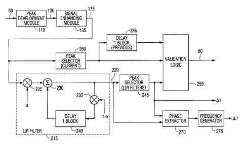
Referring to Fig. 4, the second embodiment of acquisition module 75 includes
peak development module 110 and signal enhancing module 135 as preliminary
signal
processing stages similar to the first embodiment of acquisition module 75.
However,
subsequent signal processing stages are added to validate the temporal
consistency of
the received signal. Signal 175 output from signal enhancing module 135 is
provided to
the input of an infinite impulse response (IIR) filter 215 which filters the
signal input
thereto and provides an IIR filtered signal 220 to an output thereof. The
impulse
1 o response of the IIR filter is such that the most recently received signals
input thereto are
weighted more heavily than the previously received signals input thereto.
Thus, the
most recently filtered enhanced signal peaks input to IIR filter 215 are most
heavily
weighted at the output thereof.
More particularly, complex signal 175 input to IIR filter 215 comprises
contiguous blocks of cumulative signal segments of Na samples. IIR filter 215
filters
the first sample of a first block with the first samples of successive blocks,
to produce a
filtered first sample. Similarly, the second sample of the first block is
filtered with the
second samples of subsequent blocks to produce a filtered second sample, and
so on, to
produce an output IIR filtered block of cumulative signal segments of NQ IIR
filtered
2o samples. In this way, IIR filter 215 can be considered as a bank of Na IIR
filters
operating in parallel, each of the parallel filters filtering samples
occupying the same
predetermined position within each of the contiguous blocks of cumulative
signal
segments containing Na input samples.
In detail, within IIR filter 215 are a first-stage coefficient multiplier 225
for
multiplying coefficient a against samples of filtered, complex signal 175, and
a
subsequent accumulator 230 which accumulates the weighted samples output by
coefficient multiplier 225, and the delayed, weighted samples output by
feedback delay
circuit 240. Second stage coefficient multiplier 235, which weights
accumulated output
samples by a predetermined factor, 1-a, and feedback delay circuit 240,
together provide
3o IIR filter functions well known in the art of IIR filters. However, it
should be
CA 02362029 2001-08-17
WO 00/49782 PCT/US00/04062
23
appreciated that the time delay imparted to feedback samples by feedback delay
circuit
240 corresponds to the cumulative period or duration of the predetermined
number of
boundary signal segments that are additively superimposed by additive
superposition
module 140. For instance, where a block of 32 segments are additively
superimposed,
the 1 block delay imparted by delay circuit 240 is 32 x T (an Na =1080 sample
symbol
period).
IIR filtered signal 220 output from IIR filter 215, similar to the filtered,
complex
signal I75 input to the IIR filter, comprises complex signal samples extending
across
contiguous IIR filtered cumulative signal segments, each segment having a full
symbol
to period Ta and including a signal peak therein. Thus, symbol timing
continues to be
preserved at the output of the IIR filter.
Peak selector 245, operating similar to peak selector 190 described
previously,
establishes the temporal position of each IIR filtered signal peak input
thereto, and
provides this temporal position or sample index, to validation logic module
255. When
validated, this temporal position is used as the symbol timing offset Ot, and
the phase, as
determined at the validated signal peak output from the IIR filter, is used
for
determining the carrier frequency error, by the method described previously in
relation
to Fig. 3.
Complex signal 175 is further provided as an input to peak selector 260, which
2o establishes the temporal position of the enhanced signal peak present in a
current
cumulative signal segment of signal 175. This current cumulative signal
segment
represents the accumulation of the most recently received block of
superimposed
boundary signal segments. The current temporal position is provided to an
input of
validation logic module 255.
In addition to providing the current temporal position to an input of
validation
logic module 255, the previous temporal position, that is, the temporal
position of the
enhanced signal peak in the cumulative signal segment immediately preceding
the
current cumulative signal segment, is developed and provided as an input to
validation
logic module 255. This immediately preceding or previous cumulative signal
segment,
3o and the previous enhanced signal peak therein, represents an accumulation
of the block
CA 02362029 2001-08-17
WO 00/49782 PCT/US00/04062
24
of boundary signal segments immediately preceding the most recently received
block
thereof. Stated otherwise, and by way of specific example, the current
temporal position
represents the enhanced signal peak for the most recently received contiguous
block of
32 superimposed boundary signal segments, while the previous temporal position
is
representative of the immediately preceding 32 superimposed boundary signal
segments.
The previous temporal position is developed by imparting a time delay to the
present temporal position. The time delay corresponds to the cumulative period
of one
block (the predetermined number) of boundary signal segments that are
additively
superimposed to develop a cumulative signal segment. In the example above,
this time
delay corresponds to 32 x Ta (an Na 1080 sample symbol period). Delay circuit
265
provides the requisite delay to the current temporal position input thereto,
and provides
at its output the previous temporal position, that is then input to validation
logic module
255.
In brief summary of the foregoing, the following set of temporal positions are
provided as inputs to validation logic module 255:
1) The IIR temporal position, corresponding to the position of the IIR
filtered signal peak in the most recently provided IIR filtered signal segment
(output
from the IIR filter);
2) The current temporal position, corresponding to the position of the
signal peak in the most recently provided cumulative signal segment; and
3) The previous temporal position, corresponding to the position of the
signal peak in the immediately preceding cumulative signal segment.
Validation logic module 255 performs a predetermined temporal or positional
correlation between the inputs thereto to establish whether the signal peaks
output by
IIR filter 215, as indicated at the output of peak selector 245, are
temporally valid.
Specifically, validation logic module 255 determines whether both the current
and
previous signal peak positions are aligned within a predetermined number of
samples,
for example, 10 samples, with respect to the IIR signal peak position. If they
are, then
the temporal position of the IIR filtered signal peak is determined valid and
is used for
CA 02362029 2001-08-17
WO 00/49782 PCT/US00/04062
symbol timing purposes. Additionally, the validated IIR filtered signal peak,
corresponding to this validated temporal position, is used to determine
carrier frequency
error in the same manner as was described previously, using phase extractor
270 and
frequency generator 275 (FIG. 4).
5 Referring to both Figs. 2 and 4, after the temporal position has been
validated,
validation logic module 255 of acquisition module 75 indicates such validation
to
control and tracking module 85 by way of acquisition status signal 80. In
turn, control
and tracking module 85, via demodulator control signal 90, enables the
demodulation
process as executed by OFDM demodulator 100. Whether validation logic module
255
to is partitioned to exist within acquisition module 75 or within control and
tracking
module 85, and the specific mechanism by which OFDM demodulator 100 or the
demodulation produced thereby, is enabled, are not important to the specifics
of the
present invention. What is important in the second embodiment of acquisition
module
75 is that the acquisition process be validated to thus indicate successful
acquisition of
I S symbol timing offset and carrier frequency error as a prerequisite to the
acceptance of
demodulated data output from OFDM demodulator I00, as optimally demodulated
data.
In the event that validation logic module 255 is unable to validate the
temporal
position of the IIR filtered signal peak, the acquisition process continues
until such time
as validation of symbol timing offset does occur.
2o The additional signal processing provided in the second embodiment of the
acquisition module of the present invention ensures demodulation of the
received
OFDM signal only after symbol timing offset and carrier frequency error have
been
successfully recovered from the received signal. In the presence of signal
scattering,
mufti-path and other signal interference, the second embodiment provides a
level of
25 confidence that the received symbol demodulator in the receiver provides
correctly
demodulated data at the output thereof.
By further providing a receiver that employs diversity selection and combining
between redundantly transmitted and received signals, the ability of the
receiver of the
present invention to combat the aforementioned deleterious signal effects is
even further
3o enhanced. In the third embodiment of the present invention, such a
diversity system for
CA 02362029 2001-08-17
WO 00/49782 PCT/US00/04062
26
recovering symbol timing offset and carrier frequency error from a diversity
OFDM
signal is provided.
The OFDM modulator provided at the transmitter end of the diversity system of
the third embodiment operates in a fashion similar to OFDM modulator module
25,
discussed in relation to the first embodiment of the present invention, with
the exception
that a diversity OFDM signal is provided at the output thereof. Specifically,
the
transmitter produces and transmits to the diversity receiver of the third
embodiment an
OFDM modulated signal in both an upper and a lower frequency sideband, where
each
of the sidebands encompasses a plurality of OFDM modulated frequency Garners
(FIG.
l0 1 a), and where the sidebands together form a series of composite OFDM
symbols, as
shown in Fig. lb.
This diversity OFDM signal is transmitted by the OFDM diversity transmitter to
the OFDM diversity receiver, in the same manner as described in relation to
the first
embodiment of the present invention. It should, however, be appreciated that
in this
third embodiment, the diversity receiver includes both an upper and a lower
frequency
sideband acquisition module and additional signal processing required to
effect diversity
selection and combining between the two.
Referring to Fig. 5, in the third embodiment of the present invention, the
diversity receiver includes a front-end receiver module, not shown, that
provides a
2o received analog OFDM signal to the input of A/D 295. The sampled signal
output from
A/D 295 is provided to the input of sideband separator 300 which passband
filters both
the upper and lower frequency sidebands present in the received signal to
provide an
upper sideband signal 305 and a lower sideband signal 310 at respective
outputs thereof.
Upper sideband signal 305 is provided as an input to upper sideband
acquisition module
31 S while lower sideband signal 310 is provided as an input to lower sideband
acquisition module 320. Additionally, both signals 305 and 310 are
respectively
provided to at least one receiver circuit, such as at least one correction
circuit and/or
demodulator, etc.
Up to this point, the signal processing, as represented by A/D 295, sideband
3o separator 300 (the passband filters), and the respectively fed acquisition
modules
CA 02362029 2001-08-17
WO 00/49782 PCT/US00/04062
27
315,320, substantially replicates the signal processing described in relation
to the first
and second embodiments of the present invention, with the exception that both
upper
and lower sideband paths are presented. Stated otherwise, in the third
embodiment,
each of the upper and lower frequency sidebands are subjected to the signal
processing
stages described previously. Further, the various signals flowing between the
various
signal processing stages have the same characteristics as were previously
described.
Thus, with regard to the upper and lower sideband acquisition modules, only a
brief
description is provided for those aspects thereof that overlap earlier
description.
Returning again to FIG. 5, upper sideband signal 305 is subjected, in
sequence,
to to signal processing by peak processing module 325U, which includes both
the peak
development module and signal enhancing module described previously, and IIR
filter
module 330U which provides IIR filtered signal peaks to the output thereof for
subsequent input to peak selector 335U.
Input to upper sideband validation logic module 340U are the following
signals:
1 ) the temporal positions representing IIR filtered signal peaks output
from peak selector 335U;
2) the current temporal positions 345U of signal peaks corresponding to
the current blocks of contiguous signal segments additively superimposed by
peak
processing module 325U; and,
3) the previous temporal positions 350U of signal peaks corresponding to
the previous blocks of contiguous signal segments output from peak processing
module
325U.
Since the signal processing modules that generate signals 345U and 350U were
described previously in relation to Fig. 4, they are not redundantly
reproduced here, and
are thus omitted from FIG. 5 for purposes of descriptive expediency and
clarity.
Upper sideband validation module 340U operates in the same manner as was
described previously in relation to the second embodiment of the present
invention
(FIG. 4), and provides an upper sideband acquisition status signal 355U at an
output
thereof responsive to a positional correlation between the temporal positions
at its three
CA 02362029 2001-08-17
WO 00/49782 PCT/US00/04062
28
inputs. Upper sideband acquisition status signal 355U is provided to diversity
combining logic module 370.
Upper sideband acquisition module 315 further provides an upper sideband
symbol timing estimate OtU to the diversity combining logic module 370. The
carrier
frequency error OfU is derived by module 367U in accordance with previously
discussed
techniques. Specifically, the error is derived by module 367U, which
incorporates a
phase extractor and frequency generator therein, responsive to the IIR
filtered signal
360U and timing estimate OtU input thereto.
Having briefly described the operation of upper sideband acquisition module
Io 315, it is sufficient to appreciate that the signal processing performed by
lower sideband
acquisition module 320 proceeds in a substantially equivalent manner as in the
upper
sideband. More specifically, as between the two sidebands, operationally
equivalent
signal processing modules bear the same numeric designation in Figure 5; the
"U"
suffix designating the upper sideband, the "L" suffix designating the lower
sideband.
Lower sideband acquisition module 320 provides symbol timing estimate OtL
and a earner frequency error correction signal ~fL to diversity combining
logic module
370. Further, lower sideband validation logic module 340L provides lower
sideband
acquisition status signal 355L to diversity combining logic module 370.
The diversity receiver further includes a signal combiner 385 for combining
2o corresponding IIR filtered samples output from the IIR filters 330U,330L of
the upper
and lower sideband acquisition modules 315,320. The resultant combined signal
is
input to peak selector 390 which operates in a substantially similar fashion
to the
previously described peak selector. A combined symbol timing offset Ot~ is
output
from combined peak selector 390, and a combined carrier frequency error Of~ is
derived
and output by module 392, both of these signals being provided as inputs to
diversity
combining logic module 370. It should be appreciated that by combining upper
and
lower sideband signals, as by signal combiner 385, additional processing gain
can be
achieved, thus leading to further accuracy in both symbol timing offset and
carrier
frequency error estimation, as represented by ~t~ and Of~, respectively.
CA 02362029 2001-08-17
WO 00/49782 PCT/US00/04062
29
As illustrated in FIG. S, the diversity receiver includes diversity combining
logic
module 370, which has input thereto the following signals:
1) upper and lower sideband status signals 355U and 355L;
2) upper and lower sideband symbol timing offsets OtU and OtL;
3) upper and lower sideband Garner frequency errors OfU and dfL; and,
4) combined symbol timing offset ~t~ and combined carrier frequency
Of~.
Responsive to these inputs, diversity combining logic module 370 provides at
outputs thereof a diversity signal 375, timing offset 0t, and carrier
frequency error ~f.
to Diversity status signal 375 is provided as an input to diversity receiver
controller
module 380, whereas the timing offset and frequency error are provided to the
demodulation processing module to correct timing and frequency, as described
previously.
Diversity combining logic module 370 provides the diversity combining signal
processing required to select the appropriate signal pair, consisting of a
symbol timing
offset and a corresponding carrier frequency error, from either the upper or
the lower
frequency sideband acquisition module, or from a combination of both (the
combined
signal pair), or as the case may be, to determine that further acquisition is
required.
Essentially, module 370 serves as a "smart" multiplexer to conditionally
select between
the three symbol timing offset and carrier frequency error pairs input
thereto, for its
outputs t and f.
In the operation of the diversity receiver, each receiver sideband, including
the
upper and lower sideband acquisition modules, operate, for the most part,
independently
with respect to each other. Each of the validation logic modules 340U and 340L
operate
as described in the second embodiment (Fig. 4), providing as outputs their
respective
acquisition status signals 355U, 355L. That is, upper sideband validation
logic module
340U validates upper frequency sideband symbol timing offset, as represented
by
temporal positions output by peak selector 335U, and lower sideband validation
logic
module 340L validates lower frequency sideband timing offset, as represented
by the
temporal signal peak positions output from peak selector 335L.
CA 02362029 2001-08-17
WO 00/49782 PCT/US00/04062
Referring to FIG. 8, which represents the decisional and selection
(multiplexing)
logic executed by diversity combining logic module 370, module 370 performs
the
following decisional (validation) steps, and responsive thereto, selects the
following
symbol timing offset and Garner frequency error for output therefrom:
5 1 ) upper sideband symbol timing offset OtU and carrier frequency ~fU
are selected for the demodulation process if upper sideband acquisition status
signal
355U indicates valid upper sideband symbol timing offset, and lower sideband
acquisition status signal 355L indicates invalid lower sideband symbol timing
offset
(FIG. 8, blocks 500 and 505);
l0 2) lower sideband symbol timing offset OtL and carrier frequency error
OfL are selected for the demodulation process if lower sideband acquisition
status signal
355L indicates valid lower sideband symbol timing offset, and upper sideband
acquisition status signal 355U indicates invalid upper sideband symbol timing
offset
(FIG. 8, blocks 510 and S 1 S);
15 3) if the upper and lower sideband symbol timing offsets are both
validated, then diversity combining logic module 370 determines whether a
predetermined temporal correlation exists between the validated upper and
lower
sideband symbol timing offsets. That is, if the upper and lower sideband
symbol timing
offsets are within a predetermined number of samples of each other, for
example, 10
2o samples, then combined symbol timing offset dt~, as established at the
output of peak
selector 390, and combined carrier frequency error Of~, as established at the
output of
module 392, are selected for the demodulation process (FIG. 8, blocks 520, 525
and
530); and
4) if the upper sideband and lower sideband symbol timing offsets are
25 both validated (as in the previous step), but the upper and lower sideband
symbol timing
offsets are not temporally correlated, or if neither of the sideband signal
timing offsets
are validated (according to the previous step), then no symbol timing offset,
nor any
carrier frequency error, is selected and the acquisition process continues
(FIG. 8, blocks
520, 525 and 535).
CA 02362029 2001-08-17
WO 00/49782 PCT/US00/04062
31
Since the combined signal peak is formed as an additive combination of the
temporally correlated upper and lower sideband signal peaks, and since the
temporal
positions of these upper and lower sideband signal peaks are known, then the
temporal
position of the combined signal peak is necessarily constrained to lie within
a
predetermined range of positions, relative to its constituent signal peaks.
Thus, peak
selector 390 need only search within this predetermined range of positions,
say 50
samples either side of an upper or lower sideband temporal position, in order
to find and
establish the temporal position of the combined signal peak. By limiting the
range of
search, processing time, and acquisition time is reduced, thus increasing the
overall
to efficiency of the process.
Diversity combining logic module 370 can be implemented as discrete digital
logic (AND, OR, NOR, XOR, etc.), gate array logic, software modules executing
on a
processor, a combination of the foregoing, or using any other conventional
approach.
Further, it should be appreciated that, in the present invention, the
particular partitioning
of logic functionality between the upper and lower sideband validation logic
modules
and the diversity combining logic module is exemplary. Any alternative
arrangement
can be used, provided the overall validation and selection logic functions are
preserved.
In brief summary of the operation of module 370, if only one of the sidebands
has a valid symbol timing offset, then such is used for demodulation. On the
other
. hand, if each sideband has a valid symbol timing offset, and these valid
symbol timing
offsets are temporally correlated in accordance with a predetermined criteria,
then IIR
filtered signal samples taken from each sideband are combined, and the symbol
timing
generated therefrom, that is, a combined symbol timing offset and frequency
error, is
chosen for the demodulation process. If, on the other hand, each sideband is
validated,
but the sidebands are not temporally correlated each to the other, or if
neither sideband
is validated, then no symbol timing offset is chosen, and acquisition
continues.
Throughout this process, diversity receiver controller 380 asserts the
requisite
control over the receiver circuits to control the operation thereof in
accordance with
selection outputs 375 provided by diversity combining logic module 370.
CA 02362029 2001-08-17
WO 00/49782 PCT/US00/04062
32
In summary, the diversity method of the present invention for recovering
symbol
timing offset and Garner frequency error from the OFDM signal, comprises the
steps of:
transmitting the OFDM modulated signal in both an upper and a lower
frequency sideband, each of the sidebands encompassing a plurality of OFDM
modulated frequency carriers and a series of OFDM symbols;
receiving the OFDM modulated signal of the upper frequency sideband
and providing a first (upper sideband) received signal output and the OFDM
modulated
signal of the lower frequency sideband and providing a second (lower sideband)
received signal output;
to developing a first (upper sideband) symbol timing offset and frequency
error corresponding to OFDM symbols in the first received signal;
developing a second (lower sideband) symbol timing offset and
frequency error corresponding to OFDM symbols in the second received signal;
validating the first symbol timing offset based on a predetermined
temporal consistency thereof;
validating the second symbol timing offset based on a predetermined
temporal consistency thereof;
selecting an optimum symbol timing offset from the first and second
symbol timing offsets responsive to the validating steps; and,
2o demodulating a series of OFDM symbols of at least one of the sidebands
using the optimum symbol timing offset.
The method also includes the steps of developing a third (combined) symbol
timing offset corresponding to a combination of first and second timing
signals
respectively representative of the first and second symbol timing offsets;
and,
selecting the third symbol timing offset as the optimum symbol timing
responsive to predetermined timing conditions.
The diversity combining architecture and methodology described above provides
a robust receiver acquisition system wherein symbol timing and carrier
frequency can be
successfully recovered even when an entire sideband is blocked as by a fade or
3o interference. On the other hand, by combining upper and lower sideband
signals, as by
CA 02362029 2001-08-17
WO 00/49782 PCT/US00/04062
33
signal combiner 385, additional processing gain can be achieved when the
combined
symbol timing (output from peak selector 390) is utilized.
Throughout the foregoing detailed description of the present invention, the
various signal processing modules operate on the received, sampled OFDM
signal,
comprising the series of OFDM symbols. It is most important to appreciate that
it is the
OFDM modulator and not the receiver that establishes the predetermined number
of
samples in each symbol, such as the 1080 samples used for illustrative
purposes. The
sample rate at the receiver, as determined at A/D 50, which in turn
establishes the actual
number of received samples for each received symbol, is set based upon a
variety of
l0 criteria not important to the salient features of the present invention,
including for
instance the Nyquist criteria, etc. A/D 50 can either under or over-sample the
received
symbols in establishing the number of received samples per symbol, or
alternatively,
can generate the same number of samples per symbol at the receiver as were
established
at the modulator.
What is important in the signal processing of the present invention, is that
the
symbol timing be preserved at each respective stage thereof. So long as each
stage of
processing is based upon a symbol period's worth, or multiple thereof, of
received
samples, it matters not whether this number of samples is below, the same as,
or above
the number of symbol samples established at the modulator; symbol timing will
always
2o be preserved. In summary, the foregoing descriptions of the detailed
embodiments in no
way limit the possible variations of the received signal sample rate in the
present
invention.
Extending this concept further, the preservation of symbol timing throughout
each of the signal processing stages can be achieved under a variety of
embodiments of
the present invention, not previously described. Again, so long as signal
processing is
based upon a symbol period's worth, or multiple thereof, of samples, then, for
instance,
the additive superposition module need not accumulate each sample input
thereto.
Every other or every third sample, for example, could be accumulated over a
symbol
period. Further, the boundary signal segments accumulated to produce a
cumulative
3o signal need not be contiguous; every other or every third segment, for
example, could be
CA 02362029 2001-08-17
12-04-2001 US 000004062
l _. __. _ _ _ _: _5: 45 FAg 412 568 8099 ECRERT SEAMANS
34
be superimposed, so long as the approach is consistently applied to alt
incoming boundary
_ siGnal segmcxits_
Another alternative embodiment of the presc~ invention stems from the linear,
and
thus interchangeable, nature of both the additive superposition and matched
filter processes.
Although it is preferable to precede matched filtering with additive
superposition in the
pxesent invention, such is not a limitation thereof. Their sequencing can be
swapped, to
thus provide matched filtering prior to additive superposition.
Note that the signal processing circuits or modules in each of the embodiments
of
the present invention, including but not being limited to the peak development
module,
additive superposition and matched filter modules of the signal enhanceatent
module, peak
selector, . phase cxnractor and frequency generator, validation logic module,
diversity
corubining Iogic module, OFDM modulator module, and all of the circuits
constituting the
foregoing modules can be implemented using a variety of techniques and
technologies.
The modules can be implemented as digital Iogic in gate arrays, application
specific
1S integrated circuits, fcld programmable gate arrays such as are provided by
Zilinx Corp.,
programmable Iogic arrays and devices, etc.
Alternatively, the modules can be implemented as programs executing on
computer
hardware platforms such as custom built or commercially available digital
signal processors
or microprocessors.
Further, the signal processing modules can 1~e implemented exclusively as
computer
program routines that execute on a computer workstation, for applications
including, for
example, sineulations. '
Even further, analog processing can replace digital processing if desired.
The overall system of the present inventio~o can be implemented using a
virtually
unlimited combination of the foregoing exemplary technologies.
Although this invention bas been described ire connection with . specific
forms and
crnbodi~ment thereof, it will be appreciated thzt various modifications other
than those
discussed above may be resorted to without departing from the invention. For
exampie,
functionally equivalent elements may be substituted ~or
AMENDED SHEET
CA 02362029 2001-08-17
112_04_2001 3;45 FAa 412 588 8099 ECKERT SEAMANS US 000004062
.those Specifically shown. and descr'bed, proportional quantities of the
elements shown and
described rnay be varied, and in the formation method steps described,
particular steps may
be reversed or intcrposed, all without dcparting from the invcntion as defiaed
iaa the
appended claims.
AMENDED SHEET