Note: Descriptions are shown in the official language in which they were submitted.
CA 02362062 2001-07-06
WO 00/41292 PCT/CA00/00007
-1-
Title: SELF OSCILLATING POWER CONVERTER CIRCUIT
FIELD OF THE INVENTION
The present invention relates generally to self oscillating power
converters and more particularly to an improved self oscillating circuit for
power converters.
BACKGROUND OF THE INVENTION
As the number of electronic devices continue to multiply in
residential and office environments, the adverse effects of electro-
magnetic interference (EMI) noise from one piece of equipment on other
nearby equipment are becoming more problematic. As a result, restrictions
on permissable EMI levels produced by electronic devices are becoming
more stringent which in turn is producing significant demand for high-
efficiency power converters with appropriately reduced EMI emissions.
Forced oscillation converters are commonly used in high efficiency
power supplies. This type of converter generally comprises an input
rectifier and filter, high frequency inverter, control circuit and an output
section. Typically, high frequency MOSFET switches are operated by
varying duty cycle or frequency to maintain the output voltage at a desired
level. The efficiency of such converters is limited by losses in the
MOSFETs during turn-on and turn-off, particularly in pulse-width
modulated (PWM) converters. Since the primary current of a power
transformer is periodically interrupted by high voltage spikes, EMI is
produced. In the case of balanced converters, it is difficult to achieve
synchronized opening and closing of the MOSFET switches due to stray
capacitances, inductance and noise, complex control circuitry for providing
properly formed and timed DC pulses is generally required. These
conditions require the addition of numerous interference suppressor and
protection circuits and result in increased converter size and complexity.
Methods for reducing EMI for forced oscillation power converters include
the use of snubbers, input filters as well as adoption of special control
strategies. However, these methods further complicate the design process
and appreciably increase production cost.
CA 02362062 2001-07-06
WO 00/41292 PCT/CA00/00007
-2-
Self oscillating converters do not utilize as many components as
forced oscillation converters and may not generate such high levels of
EMI, however they suffer from switching speed limitations and power
inefficiencies. Transformer coupled self oscillating converters are designed
to trigger switching transistor turn-on and turn-off using either the
saturation of the switching devices, saturation of the power transformer
core, or saturation of an intermediate drive transformer. The technique of
saturation switching transistors is limited to slower switching speeds and
the energy required to fully saturate transformers causes power losses and
results in compromised efficiencies.
Specifically, a longstanding type of self oscillating DC to DC
converter is disclosed in U.S. Patent No. 5,303,137 to Peterson. Peterson
utilizes a MOSFET half-bridge configuration in which each transistor is
alternately saturated. Once a transistor is saturated, current continues to
flow in the transformer winding due to the magnetizing inductance of the
transformer and the reflected load current. This current discharges the
voltage across a circuit capacitor to reduce the voltage across the primary
winding, which in turn is coupled to the gate windings. As the current
rises, the transistor comes out of saturation and turns itself on again
causing a voltage drop to reappear across the transformer. However, since
this switching technique relies on the transistor beta factor it cannot be
implemented using MOSFETs and higher switching frequencies cannot be
achieved.
Another type of self oscillating circuit drives transistor switches
using the properties of core saturation, as described in U.S. Patent No.
4,319,315 to Keeney, Jr. et al., where a DC to DC converter uses a saturable
transformer having a center-tap and resistive network interposed among
four sequentially operating transistors. The transistors cause one side of
the input DC voltage to be sequentially applied to opposite sides of a
primary winding of the transformer which, in turn, cause the transformer
to be excited into positive and then negative saturation conditions. When
the transformer core saturates, appropriate gate drive voltages collapse and
the associated transistors switches are turned off. While core saturating
CA 02362062 2001-07-06
WO 00/41292 PCT/CA00/00007
-3-
transformer converters are simpler than forced oscillating converters,
since the core must be fluxed from one end to another in order to fully
saturate, significant power losses result and overall efficiency is reduced.
Finally, another type of self oscillating converter utilizes resonance
effects within an oscillating circuit, such as the converter disclosed in U.S.
Patent No. 5,430,632 to Meszenyi where a pair of MOSFET transistors are
configured in a half-bridge configuration and coupled to a reactive
network. The frequency of oscillation is determined by the gate-to-source
capacitance of the transistors and the inductance of the drive transformer.
This resonance converter suffers from increased complexity, sensitivity to
parasitics and emissions due to its high operating frequency.
Thus, there is a need for a self oscillating power converter which
achieves conventional power efficiencies using a minimal number of
parts, which generates a significantly reduced amount of EMI, which
provides increased reliability, and which can be operated at slower
switching speeds to further reduce EMI emissions.
BRIEF SUMMARY OF THE INVENTION
Accordingly, it is an object of the present invention to provide a
relatively simple self-oscillating DC power converter circuit which
oscillates at lower switching speeds to provide reduced EMI and has a non
saturating transformer to reduce power losses.
One embodiment of a circuit according to the present invention
provides a DC output voltage which corresponds to a DC input voltage.
The input DC voltage is alternately switched across a pair of primary
windings of a transformer. A secondary output winding is coupled to each
of the primary windings. A secondary voltage appears across each of the
secondary output windings as the input DC voltage is switched across the
corresponding primary winding. The secondary voltages are rectified and
provide the DC output voltage. The DC output voltage corresponds to the
input DC voltage, based on the turns ratio of the primary windings to the
secondary output windings. The switching of the input DC voltage across
the primary windings is controlled by alternately switching two MOSFET
CA 02362062 2001-07-06
WO 00/41292 PCT/CA00/00007
-4-
transistors. Each transistor is coupled to one primary winding so that a
greater amount of the DC input voltage is seen across the corresponding
primary winding as the transistor is turned on. When the transistor is
. fully on, essentially the entire input DC voltage is seen across the primary
winding. The gate of each transistor is coupled to a gate drive winding
which is transformer coupled to the primary winding controlled by the
transistor. The transistor is turned on by charging its gate capacitance
through the gate driving winding. As the transistor is turned on, the
voltage across the primary winding increases, thereby increasing the
voltage across the gate drive winding, which turns on the transistor at an
increasingly accelerated rate. After the transistor has fully turned on, it is
switched off by isolating the gate from the gate drive winding using a
capacitor and discharging the gate capacitance through a discharge resistor.
This turn off process is performed slowly to reduce EMI radiation.
The production of EMI is further diminished by a transformer
isolating both of the switching transistors from the secondary output
windings, thereby allowing the transistors to be configured in a common
drain configuration.
Power losses during the turn-off process are reduced by operating
the transistor in a soft switching manner thereby reducing power
dissipation.
In one aspect of the present invention, there is provided a self
oscillating power converter circuit having: a source of direct current
voltage; a drive transformer having first and second primary windings
and a first control terminal winding for generating a first control voltage,
said first control terminal winding being transformer coupled to said first
primary winding; first and second transistors connected across said first
and second primary windings, said first transistor having a first control
terminal coupled to said first control terminal winding, said first control
terminal having a first control terminal capacitance, said first control
terminal capacitance being charged in response to said first control voltage,
and said first and second transistors alternately being turned on and off; a
first feedback path for said first transistor including said first control
CA 02362062 2001-07-06
WO 00/41292 PCT/CA00/00007
-5-
terminal winding, said first control terminal winding being phased with
said first primary winding such that said direct current voltage provides
regenerative feedback at said first transistor control terminal; a first
resistance coupled between said first control terminal and said first
primary winding for discharging said first control terminal capacitance,
and; a first coupling capacitance coupled to said first transistor control
terminal for allowing said first control terminal capacitance to be
discharged through said first resistance, wherein said first transistor turns
on in response to the charging of said first control terminal capacitance
and turns off in response to the discharging ~of said first control terminal
capacitance.
A second aspect of the present invention provides a self oscillating
power converter circuit having: a source of direct current voltage; a drive
transformer having first and second primary windings; first and second
transistors connected across said first and second primary windings, said
first transistor having a first control terminal, said second transistor
having a second control terminal, said first control terminal having a first
control terminal capacitance and said second control terminal having a
second control terminal capacitance; a first feedback path for said first
transistor including a first coupling capacitor and said first and second
primary windings and a second feedback path for said second transistor
including a second coupling capacitor and said first and second primary
windings; and a first resistor coupled to said first control terminal and to
said second transistor for discharging said first control terminal capacitance
and a second resistor coupled to said second control terminal and to said
first transistor for discharging said second control terminal capacitance.
A third aspect of the present invention provides a self oscillating
power converter circuit having: a source of direct current voltage; a drive
transformer having a primary winding and a first control terminal
winding for generating a first control voltage, said first control terminal
winding being transformer coupled to said primary winding; first and
second transistors connected across said primary winding, said first and
second transistors alternately turning on and off, said first transistor
CA 02362062 2001-07-06
WO 00/41292 PCT/CA00/00007
-6-
having a first control terminal coupled to said first control terminal
winding and said first control terminal having a first control terminal
capacitance, said first control terminal capacitance being charged in
response to said first control voltage; a first feedback path for said first
transistor including said first control terminal winding, said first control
terminal winding being phased with said primary winding such that said
direct current voltage provides regenerative feedback at said first transistor
control terminal; a first coupling capacitance coupled to said first
transistor
control terminal within said first feedback path for allowing said first
control terminal capacitance to be discharged; and a first resistor coupled to
said first control terminal and to said primary winding for discharging said
first control terminal capacitance, wherein said first transistor turns on in
response to the charging of said first control terminal capacitance and
turns off in response to the discharging of said first control terminal
capacitance.
Further objects and advantages of the invention will appear from
the following description, taken together with the accompanying
drawings.
BRIEF DESCRIPTION OF THE DRAWINGS
In the accompanying drawings:
Fig. 1 is a circuit diagram of a preferred push-pull embodiment of
the self oscillating power converter of the present invention;
Fig. 2 is a graph showing the voltage across primary transformer
windings TB and T~;
Fig. 3 is a graph showing the gate voltage of a transistor Q4 and
across gate drive transformer winding TA;
Fig. 4 is a graph showing the gate voltage of a transistor Q5 and the
voltage across gate drive transformer winding TD;
Fig. 5 is a graph showing the gate voltage of transistor Q4, current of
transistor Q4, and voltage across primary transformer winding TB;
Fig. 6A is a graph showing the waveform characteristics of the gate
voltage of transistor Q4 when the power converter is operating in a
CA 02362062 2001-07-06
WO 00/41292 PCT/CA00/00007
-7-
balanced manner; and
Fig. 6B is a graph showing the waveform characteristics of the gate
voltage of transistor Q4 during unbalanced operating conditions.
Fig. 7 is a circuit diagram of another embodiment of the self
oscillating power converter of the present invention implemented to
reduce the variation of the oscillation frequency when the load or input
voltage is varied.
Fig. 8 is a circuit diagram of another embodiment of the self
oscillating power converter of the present invention implemented as a
common source push-pull power converter;
Fig. 9 is a circuit diagram of another embodiment of the self--
oscillating power converter of the present invention implemented as a
push-pull power converter with minimal components;
Fig. 10 is a circuit diagram of another embodiment of the self
oscillating power converter of the present invention implemented as a
capacitive coupled push-pull power converter;
Fig. 11 is a circuit diagram of another embodiment of the self-
oscillation power converter of the present invention implemented as a
hybrid transformer and capacitive coupled push-pull power converter;
Fig. 12 is a circuit diagram of another embodiment of the self-
oscillation power converter of the present invention implemented as a
transformer coupled full-bridge power converter; and
Fig. 13 is a circuit diagram of another embodiment of the self-
oscillation power converter of the present invention implemented as a
transformer coupled half-bridge power converter;
Fig. 14 is a circuit diagram of another embodiment of the self-
oscillation power converter of the present invention implemented as a
hybrid transformer and capacitive coupled full-bridge power converter;
and
Fig. 15 is a circuit diagram of another embodiment of the self-
oscillation power converter of the present invention implemented as a
hybrid transformer and capacitive coupled half-bridge power converter.
CA 02362062 2001-07-06
WO 00/41292 PCT/CA00/00007
_g_
DETAILED DESCRIPTION OF PREFERRED EMBODIMENTS
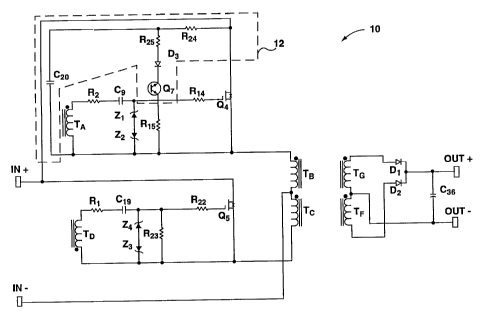
Reference is first made to Fig. 1, which a self oscillating power
converter circuit 10 made in accordance with a first preferred embodiment
of the invention. Power converter 10 is a push-pull converter which
includes a starter circuit 12, a set of primary transformer windings TB and
T~, secondary transformer windings T~ and TF and gate drive windings TA
and TD, MOSFET transistors Q4 and Q5, coupling capacitors C9 and C19,
discharging resistors R15 and R23, damping resistors R2 and Rl, gate stopper
resistors R14 and R22, and zener diodes Zl, Z2, Z3, and Z4.
Starter circuit 12 preferably comprises capacitor C2o, resistors R24 and
R25, diode D3, and diac Q~ as described in U.S. Patent No. 5,430,632 to
Meszlenyi. It should be understood that while this type of starting circuit is
preferred due to its simplicity and low cost, many other well known starter
circuits may be used to start power converter 10. Due to inevitable slight
imbalances in component values (e.g. differences in the transistor
characteristics of Q4 and Q5), it would even be possible to start the circuit
simply by raising the DC voltage rapidly across the input of power
converter 10.
Power converter 10 receives DC voltage across terminals IN+ and
IN- from a DC source, such as a battery, an AC line power applied through
a rectifier, an output stage of a power supply, or any time varying source
having constant polarity. Power converter 10 uses primary windings TB
and T~ and secondary transformer windings T~ and TF to isolate the source
from the load. It should be noted that it is possible to have two or more
sets of secondary windings so that a range of DC output voltages can be
generated. Further, gate drive windings TA and TD are transformer
coupled to primary windings TB and T~ and drive the gates of transistors
Q4 and Q5.
Drive windings TA and TD should be well-coupled to primary
windings TB and T~ (i.e. should have a coupling coefficient greater than
.999). Further, this coupling should be greater than the coupling between
gate drive winding TA and secondary windings T~ or TF, and between gate
drive winding TD and secondary windings T~ or TF (as secondary windings
CA 02362062 2001-07-06
WO 00/41292 PCT/CA00/00007
-9-
T~ and TF could themselves be coupled). This can be achieved by winding
the gate drive windings TA and TD first, winding primary windings TB and
T~ on top of the gate drive windings and then winding secondary
windings TF and T~ on top in order to preserve the coupling between
primary and secondary windings and associated load regulation. Such
coupling ensures that the gate drive windings TA and TD will be able to
reliably drive the gates of transistors Q4 and Q5 such that oscillation is
preserved and to guard against device failure due to circuit instability,
leakage inductance and ringing currents.
While transistors Q4 and Q5 are preferably implemented as n-
channel MOSFETs, it should be understood that any type of switching
element such as p-channel MOSFETs, JFETs, BJTs or IGBTs (either p-
channel or n-channel) may be used. Because the gates of transistors Q4 and
Q5 are transformer isolated, transistors Q4 and Q5 can be operated in a
common drain configuration. That is, the drains of transistors Q4 and Q5
can be tied together to a fixed DC voltage at node IN+ which results in a
self-shielding configuration which screens the noise from the rapidly
moving source, as will be explained.
The gates of transistors Q4 and Q5 are coupled to gate drive windings
TA and TD by capacitors C9 and C19 and connected through resistors R14
and R22, respectively. In turn, capacitors C9 and C19 are coupled to primary
windings TB and T~ through resistors R15 and R23, respectively. This
allows the voltage across gate drive windings TA and TD to rise through
capacitor C9 or C19 and to dissipate through resistor R15 or R23, respectively
towards the voltage across primary windings TB and T~ (depending on the
polarity of the respective windings). The values of capacitors C9, C19 and
resistors R15 and R23 should be scaled to allow for reasonable power
dissipation, as well as reasonable changes in switching speed and frequency
due to load variation.
Damping resistors RZ and Rl are coupled between gate drive
windings TA and TD and capacitors C9 and C19, respectively. The use of
appropriate values of resistors R2 and R1 together with adjustment of the
transformer turns ratio, can serve to stabilize the operation of power
CA 02362062 2001-07-06
WO 00/41292 PCT/CA00/00007
-10-
converter 10 in an overload situation and to ensure that sufficient gate
drive is provided to transistors Q4 and Q5 for full load operation.
Gate stopper resistors R14 and R22 are used to damp very high
frequency oscillations (on the order of 100 MHz) and are a conventionally
known circuit precaution when using MOSFETs. Resistors R14 and R22
create a low pass filter with the gate of the transistors Q4 and Q5 which
damps out parasitic instability while at the same time providing sufficient
current to drive the gate voltage fast enough.
Zener diode pairs Zl/Z2 and Z3/Z4 are used to clamp the maximum
voltage on the gate of transistors Q4 and Q5 to safe limits. While this effect
could be achieved using a single zener diode, the use of a pair of zener
diodes preserves the self-balancing aspect of the oscillator.
When a DC voltage is applied across terminals IN+ and IN-, starter
circuit 12 of power converter 10 operates to start power converter 10 as
follows. Capacitor C2o starts to charge with the voltage at terminal IN+
through resistor R24. As capacitor C2o is charging, the voltage applied to
diac Q~ will increase. Once the applied voltage exceeds its breakdown
voltage, diac Q~ will begin to conduct current, causing current to flow
through resistor R25, diode D3, diac Q~ and through resistor R14 into the
gate of transistor Q4. That is, the voltage across capacitor CZO will be
applied
to the gate of transistor Q4. When the voltage on the gate of transistor Q4
rises above the turn-on threshold, transistor Q4 will start to turn on. Diode
D3 is a blocking diode which guarantees that diac Q~ will not inadvertently
refire.
Once transistor Q4 begins to conduct, the DC voltage across the IN+
and IN- terminals will be applied directly across primary winding TB. Since
primary winding TB is transformer coupled to winding TA, gate drive
winding TA will begin to produce a corresponding voltage having a
positive polarity (as indicated by the dot). As the voltage across winding TB
increases, the voltage across TA will also increase and will cause increased
current to flow through resistor R2, capacitor C9 and resistor R14 to the gate
of transistor Q4. Since the increasingly positive voltage across gate drive
winding TA is applied across the gate-source junction of transistor Q4,
CA 02362062 2001-07-06
WO 00/41292 PCT/CA00/00007
-11-
transistor Q4 will continue to be turned on. This will further increase the
voltage across primary winding TB and gate drive winding TA. This
positive feedback dynamic serves to turn on transistor Q4 in an
accelerating (or regenerative) manner. As gate drive winding TD has
reverse polarity to winding TA, when positive DC voltage is applied to
winding TB, a negative DC voltage will appear across winding TD (at the
end opposite to the dot). Since a negative voltage is applied across the
gate-source junction of the transistor Q5, transistor Q5 will continue to
turn off also in a regenerative manner. This process will continue until
transistor Q4 is fully on and transistor Q5 is fully off. Here, in effect
regenerative feedback is applied to both transistors Q4 and Q5 causing one
to turn on and one to turn off.
Once transistor Q4 is fully on, the full rated DC voltage will appear
across primary winding TB and this DC voltage will remain constant as
long as transistor Q4 is fully on. At this point, the voltage across the gate
capacitance of transistor Q4 will begin to discharge through resistor R15~
The voltage on the gate of transistor Q4 will also be discharged until a
turn-off threshold is reached whereby transistor Q4 starts to turn off.
Simultaneously, the gate capacitance of transistor Q5 begins to charge up
towards ground through resistor R23. Once transistor Q4 starts to turn off,
the turn-over process of power converter 10 is initiated and transistor Q5
will start to turn on, the details of which will be described further in
relation to the voltage and current characteristics of power converter 10
below.
By alternately turning transistors Q4 and Q5 of power converter 10
on and off, the DC voltage across IN+ and IN- is alternately applied across
primary windings TB and T~. Voltages appear across secondary windings
T~ and TF in accordance with the primary/secondary winding ratio. These
voltages are rectified by output stage diodes D1 and D2 as is conventionally
known. The rectified voltage output is applied across capacitor C36 which
provides DC voltage output of power converter 10 across terminals OUT+
and OUT-. It is evident that power converter 10 cannot be regulated in one
stage using conventional means such as PWM or frequency modulation.
CA 02362062 2001-07-06
WO 00/41292 PCT/CA00/00007
-12-
Figs. 2, 3, 4 and 5 together show a number of voltage and current
characteristics of transistors Q4 and Q5, primary windings TB and T~ and
gate drive windings TA and TD which result when power converter 10
receives a 160 volt DC input at terminals IN+ and IN-, has a turns ratio of
TA to TB (and of TD to T~) of 1:6 and has components with the following
values:
Designation Description Designation Description
(or Part No.) (or Part No.)
C2o 3300 pF D1 MUR1620CT
R24 100 kS2 D2 MUR1620CT
R25 475 S2 C36 470 ~.F
D3 1N 414Q
Q~ diac
R2 220 SZ R1 220 S2
C9 2200 pF C19 2200 pF
Z1 1N5250 Z3 1N5250
Z2 1N5250 Z4 1N5250
R14 22 S2 R22 22 S2
R15 475 S2 R23 475 S2
Q4 IRF740 Q5 IRF740
Fig. 2 shows the voltages across primary windings TB and T~ which
result when transistors Q4 and Q5 are alternately turned on and off. At
point A, the voltages across both primary windings TB and T~ are at that
instant zero. At point A, both gate voltages of transistors Q4 and Q5 (VQ4
and VQ5) are zero and neither transistor is conductive which causes zero
voltage to be applied to primary windings TB and T~. As will be explained,
between point A and point C, the gate voltage VQ4 of transistor Q4 starts to
rise (either from being started by starting circuit 12 or during normal
oscillation), transistor Q4 turns on, and the gate voltage of transistor Q5
starts to fall and transistor Q5 turns off. As transistor Q4 turns on, the DC
voltage from terminals IN+ and IN- starts to be applied across primary
CA 02362062 2001-07-06
WO 00/41292 PCT/CA00/00007
-13-
winding TB (Fig. 2). As transistor Q5 turns off, the DC voltage from
terminals IN- and IN+ starts to be applied across primary winding T~ (Fig.
2). It should be noted that once transistors Q4 and Q5 are fully on and off,
respectively, the voltages across windings TB and T~ stay constant (i.e.
between points C and D) in spite of non-threshold level variations in gate
voltage.
Fig. 3 shows the voltage across gate drive winding TA and the gate
voltage VQ4 of transistor Q4. The gate voltage VQ4 of transistor Q4 is shown
to increase from point A to C (after starting) which in turn causes the
voltage across primary winding TB (Fig. 2) to increase as has been
discussed. The voltage across gate drive winding TA (Fig. 3) also increases
from point A to point C according to the appropriate turns ratio. The
increased voltage across winding TA accelerates the increase of the gate
voltage of transistor Q4 from point B to C and accordingly the gate voltage
V Q4 of transistor Q4 will follow the voltage increase across winding TA
with a slight delay due to the presence of the input capacitances of
transistors Q4 and Q5 and resistors R2 and R14. The voltage on the gate of
transistor Q4 is driven to a peak voltage value which is limited by zener
diodes Z1 and Z2.
Fig. 4 shows the voltage across gate drive winding TD and the gate
voltage VQ5 of transistor Q5. The gate voltage of transistor Q5 is shown to
decrease from point A to C which in turn causes the voltage across
primary winding T~ (Fig. 2) to decrease as has been discussed. The voltage
across gate drive winding TD (Fig. 3) also decreases from point A to point C
according to the appropriate turns ratio. The voltage across winding TD
drives the gate of transistor Q5 and accordingly the gate voltage of
transistor Q5 will follow the voltage decrease across winding TD with a
slight delay due to the presence of capacitor C19 and resistors R1 and R22.
The voltage on the gate of transistor Q5 is driven down to a low voltage
value which is limited by zener diodes Z3 and Z4.
Now referring back to Figs. 1, 2, 3 and 4, between points A and B, the
voltage across gate drive winding TA and gate voltage VQ4 of transistor Q4
(Fig. 3) gradually increase. Between points B and C, the voltages across
CA 02362062 2001-07-06
WO 00/41292 PCT/CA00/00007
-14-
primary winding TB (Fig. 2) and gate drive winding TA (Fig. 3) increase
faster than they did between points A and B. This is due to the fact that the
voltage across gate drive winding TA adds to the gate voltage VQ4 of
transistor Q4 which in turn increases the rate that transistor Q4 turns on.
Between points B and C, the slope of the voltage of gate voltage VQ4 is less
than its slope between points A and B. When transistor Q4 is driven by a
finite source impedance, the miller capacitance must be charged through
the resistances of the circuit, as is conventionally known in respect of
MOSFET transistors. This increases the rate at which DC voltage IN+ and
IN- is applied to primary winding TB all in an accelerating manner.
An analogous dynamic occurs with respect to primary winding T~
(Fig. 2) and gate drive winding TD (Fig. 4) in that these voltages both
decrease in an increasingly rapid manner between points B and C than
between points A and B. In this case, between points B and C increasingly
negative voltage is applied across gate drive winding TD which serves to
increase the rate that the transistor Q5 turns on. This increases the rate at
which DC voltage IN- and IN+ is applied to primary winding T~. Between
points B and C, the slope of the voltage of gate voltage VQ5 is less than its
slope between points A and B. When transistor Q4 is driven by a finite
source impedance, the miller capacitance must be discharged through the
resistances of the circuit, as is conventionally known in respect of MOSFET
transistors.
Referring still to Figs. 2, 3 and 4, between points C and D, the
voltages across gate drive winding TA and primary winding TB (and
correspondingly gate drive winding TD and primary winding T~) remain
constant as long as transistor Q4 remains fully on (and as long as transistor
Q5 is fully off). Accordingly, these voltages will be independent of the gate
voltages of transistors Q4 and Q5 and capacitor C9 will have a DC voltage
across it and accordingly will be discharged. Capacitor C9 will act as a open
circuit, effectively isolating the gate of transistor Q4 from gate drive
winding TA. After the gate voltage VQ4 of transistor Q4 reaches its peak
voltage (Fig. 3), resistor R15 provides a discharge path for the gate
capacitance of transistor Q~. Accordingly, the gate of transistor Q4 will
begin
CA 02362062 2001-07-06
WO 00/41292 PCT/CA00/00007
-15-
to discharge to ground at terminal IN- through resistor R15 and the gate
voltage VQ4 of transistor Q4 (Fig. 3) will exhibit a declining ramp
characteristic from points C to D. The voltage at the node between
capacitor C9 and resistor R15 will display a corresponding declining ramp
characteristic and capacitor C9 will also be charged as a result of the
voltage
across it. This continues until transistor Q4 starts to turn off at point D.
At point D, transistor Q4 starts to turn off causing a voltage drop
across transistor Q4 to begin to develop which in turn causes the voltage
across primary winding TB to begin to decrease (Fig. 2). Accordingly, the
voltage on gate drive winding TA will follow the voltage across the
primary winding TB and also start to drop (Fig. 3) according to its winding
ratio.
At point E, gate voltage VQ4 of transistor Q4 reaches a threshold
value and transistor Q4 begins to come out of its saturation state. As the
voltage drop across transistor Q4 substantially increases, the voltages across
primary winding TB and gate drive winding TA continue to decrease.
Subsequently, the gate voltage VQ4 of transistor Q4 begins to rapidly drop
due to the effect of rapidly decreasing gate voltage as a result of decreasing
voltage across gate drive winding TA. At this point, the only currents
flowing in transistor Q4 are associated circuit magnetization and leakage
inductance currents which serve to drive transistor Q4 completely off and
transistor Q5 fully on. As the voltage drops across winding TB between
points D and E, the voltage across the reverse dotted transformer coupled
gate drive winding TD correspondingly starts to rise. Accordingly, at point
D, capacitor C19 begins to charge up with the voltage across gate drive
winding TD and applies voltage to the gate of transistor Q5. The process
described above in relation to transistor Q4 repeats in respect of transistor
Q5, and turn-on of transistor Q5 is accelerated between points E to F as
transistor Q5 begins to saturate and turn on.
Finally, as previously discussed, just after point F the gate voltage
VQ4 of transistor Q4 (Fig. 3) again experiences a small characteristic voltage
step commonly associated with MOSFET's. This wiggle is due to the
charging of the miller capacitance of transistor Q4 through the resistances
CA 02362062 2001-07-06
WO 00/41292 PCT/CA00/00007
-16-
of the circuit. Specifically, just after point F on Fig. 3, the miller
capacitance
of transistor Q4 is being discharged and just after point F on Fig. 4, the
miller capacitance of transistor Q5 is being charged.
In this way, a slow turn off process is achieved for transistor Q4
between points D and E (and correspondingly for transistor Q5 at
analogous points). Traditionally, it has been thought that when a
transistor experiences a slow turn-off, significant dissipative power losses
are inevitable. However, the inventor has discovered that as the gate
voltage VQ4 of transistor Q4 decreases between points D and E (Fig. 3) the
current flowing through transistor Q4 essentially stops due to current
conditions present in winding T~, as will be explained below.
Now referring to Fig. 5, the current IQ4 and the gate voltage VQ4 of
transistor Q4 are shown. It should be noted that current IQ4 is zero between
points D and E. Between points D and E, the transconductance of transistor
Q4 decreases. That is, as transistor Q4 becomes more resistive, a voltage
drop across transistor Q4 will be produced. That in turn will mean that the
voltage across primary winding TB will be reduced. Since there is an
existing voltage across output terminals OUT+ and OUT-, any drop in
voltage across winding TB, however slight, will cause the voltage across
winding T~ to decrease below the voltage which exists across capacitor C36
(or across terminals OUT+ and OUT-). Once this voltage differential is
established, rectifiers Dl and D2 will stop current flow in the output stage.
Since the current flowing through winding T~ is reflected in
primary winding TB, the only currents left flowing through primary
winding TB will be the magnetization and leakage inductance currents that
were previously flowing within the transformers and the ringing and
parasitic parts of the circuit. Thus, as long as there is an amount of voltage
across transistor Q4 between points D and E, current will not flow through
transistor Q4 as is shown between points D and E in Fig. 5. This means that
transistor Q4 essentially operates in a high impedance state during switch
transitions. As the analogous condition exists in respect of transistor Q5,
both transistors Q4 and Q5 of power converter 10 assume a high impedance
states during switching transitions which results in very low overall
CA 02362062 2001-07-06
WO 00/41292 PCT/CA00/00007
-17-
power dissipation.
Accordingly, power converter 10 provides comparable efficiency to
that of conventional forced oscillating power converters due to its
inherent efficiency of operation while achieving softer switching
characteristics.
Further, since power converter 10 provides a soft switching
characteristic, a significant reduction in the amount of radiated EMI is
achieved. In the example implementation of the common-drain self
oscillating power converter 10, the radiated EMI associated with power
converter 10 was determined to be 40 dB less than the radiated EMI
generated by a typical forced oscillation power converter. This reduction in
EMI emissions can be explained by two phenomena.
First, since the voltage across transistor Q4 drops as the transistor Q5
is turned on and vice versa, minimal ringing is caused in the circuit and
leakage spikes are avoided. Further, the slow rise and fall time voltage
waveforms generate less radiated noise and since leakage inductance is not
forced to stop suddenly, minimal ringing transients are produced. As
previously discussed, the energy generally produced by leakage inductance
is often recovered by adding in extra components which adds to the
complexity of the circuit. In the present case, such measures are not
required.
Second, since transistors Q4 and Q5 are transformer isolated from
secondary windings TF and T~, they can be configured in a common drain
configuration. As is conventionally known, if the voltage on the drain
moves rapidly, the voltage on the large surface area of the transistor tab
changes rapidly causing radiation of EMI noise. In addition, since the drain
is physically close to the heat sink, it is capacitively coupled to the heat
sink and radiates to the heat sink, causing more radiation of EMI. In a
common drain configuration, the voltage on the drains (the tabs of the
transistors) will be stationary and coupled to the heat sink. Since the
sources are physically separated from the heat sink by the drains (having a
larger surface area than the sources), a self-shielding effect is produced. It
should be noted that self-oscillating power converters generally have a
CA 02362062 2001-07-06
WO 00/41292 PCT/CA00/00007
-18-
common-source configuration in which the drain (on which voltage is
.. moving) provides a long path for the high-frequency current and
accordingly couples EMI noise to the circuit. In contrast, switching
transistors Q4 and Q5 of power converter 10 are self-shielding and
significantly reduce circuit radiated EMI.
A typical balanced power converter contains circuit imbalances
which can lead to inefficient or destructive switching conditions. Forced
oscillation power converters attempt to compensate for circuit inequalities
by either forcing a switching transistor on longer or shorter than the other
switching transistor. If one transistor is left on longer than another then
there is a period where all the circuit currents and voltages are forced to
stop. If one transistor is left on shorter than another then there is a period
of time where both transistors will be on which can lead to destruction of
the circuit. In contrast, the self oscillating dynamic allows each transistor
to
switch at its own speed which results in optimal right turn-on and turn-off
current and voltage characteristics and a soft switch dynamic. While it is
conventionally known that slow switching generally causes a high
amount of power dissipation, the soft switching achieved by power
converter 10 generates low power dissipation due to zero transistor
currents during switching transitions.
Power converter 10 also exhibits self-balancing behaviour which
prevents destructive core saturation. Typical push-pull converters must
maintain a zero DC component across each half-winding (otherwise flux
density builds in the transformer). When the on-time and off-time of
switching transistors are not exactly equal, increased volt seconds will tend
to build up across one of the two winding with each cycle. This will result
in an increase in core flux until the core finally saturates. .
Fig. 6A illustrates the gate voltage of transistor Q4 of power
converter 10 under balanced conditions where the on-time and off-time of
transistors Q4 and Q5 are equal. Accordingly, the average voltage will be
zero. Since gate drive windings TA and TD are transformer coupled, no net
DC voltage can be generated and thus the average voltage on each gate
drive winding must be zero. If the on-time and off-time of transistors Q4
CA 02362062 2001-07-06
WO 00/41292 PCT/CA00/00007
-19-
and Q5 are unequal (Fig. 6B) then non-equal volt seconds will tend to shift
the DC operating point of the gate drive voltage waveforms in the
negative direction such that the volts seconds across the gate drive
windings TA and TD will re-equalize. In the case shown in Fig. 6B, the
resulting gate voltage VQ4 will result in transistor Q4 turning off sooner to
rebalance power converter 10.
As an illustration, if resistor R15 has a larger value than R23, then it
will take longer to discharge capacitor C9 than it will to discharge capacitor
C19. Thus, the on-time for Q4 will be longer than the on-time for Q5. Thus,
the voltage at the gate of transistor Q4 (or the voltage across gate drive
winding TA) can be represented by the waveform of Fig. 6B. Due to the fact
that the circuit is AC coupled (through capacitors C9 and C19), the areas
under the voltage waveform must be equal. Therefore, resistor R15 will
have to discharge C9 and the gate capacitance of transistor Q4 less to reach
the transistor turn-off threshold as the threshold voltage for transistor Q4
will be lowered (see Fig. 6B). Thus, even if transistor Q4 starts off being on
longer than transistor Q5, the circuit will rapidly rebalance itself. This
feature is important, since in practice, there are many small circuit
parameters which can cause a circuit imbalance (such as the values of the
capacitors and resistors, the leakage inductance of windings TA and TD,
etc.)
Finally, a built-in safety feature prevents damage of power converter
10 due to core saturation (due to improper design parameters,
inappropriately slow switching frequencies, etc.) In the case where the core
begins to saturate, the voltage on the appropriate gate drive winding TA or
TD will rapidly drop. This will initiate turnoff of transistor Q4 or Q5 and
turnon of the complimentary transistor, which will alleviate the core
saturation.
Referring now to Fig. 7, a second exemplary self oscillating power
converter circuit 50, made in accordance with the present invention. This
circuit contains identical components to those of power converter 10 of
Fig. 1 and they are identified as such. While starting circuit 12 is not
shown, it should be understood that starting circuit 12, or any equivalent
CA 02362062 2001-07-06
WO 00/41292 PCT/CA00/00007
-20-
circuit, could be implemented within power converter 50 as before. The
only difference between power converter 50 and power converter 10 is that
coupling capacitor C9 has been moved and is now coupled between zener
diode Z1 and resistor R14. Coupling capacitor Cl9 is similarly coupled
between zener diode Z4 and resistor R22.
In power converter 10, the oscillating frequency will vary,
depending on the load coupled at terminals OUT+ and OUT-. A higher
load will result in a lower voltage across gate drive winding TA (and across
gate drive winding TD). This will in turn result in a lower voltage across
coupling capacitor C9, which will have a commensurately lower charge on
it. Coupling capacitor will discharge more quickly through resistor R15, as
described above (between points C and D in Figs. 2-5). Transistor Q4 will
begin to turn off earlier (i.e. point D will occur sooner), and the
oscillating
frequency of power converter 10 will be higher. Coupling capacitor C19,
resistor R23 and transistor Q5 will exhibit the same behaviour during the
other half of the oscillation cycle of power converter 10.
In power converter 10, the oscillating frequency also has an inverse
relationship to the magnitude of the input DC voltage across terminals
IN+ and IN-. A greater input DC voltage will result in a greater voltage
across primary winding TB when transistor Q4 is conducting and across
primary winding T~ when transistor Q5 is conducting. This will in turn
result in a greater voltage across gate drive windings TA and TD, with the
opposite effect to that described above in the case of an increased load.
In power converter 50, the dependency of oscillating frequency on
both the load and the input DC voltage is diminished by using zener
diodes Z 1 and Z2 to clamp the voltage across gate drive winding TA. This
essentially fixes the maximum voltage across coupling capacitor C9,
substantially reducing the effects of varying either the load or the input DC
voltage.
To enjoy the benefit of this improvement, zener diodes Zl and Z2
and the turns ratio of TA to TB must be selected to ensure that zener diode
Z1 is reverse biased (i.e. it is operating in its breakdown region). The
capacitance of capacitor C9 must also be increased to compensate for the
CA 02362062 2001-07-06
WO 00/41292 PCT/CA00/00007
-21-
reduced drive voltage across it. This improvement also allows the
resistance of damping resistor R2 to be increased, resulting in lower power
dissipation in power converter 50 and increasing the stabilizing effect of
the resistor. It will be apparent that similar components selections must be
selected for zener diodes Z3 and Z4, coupling capacitor C19 and damping
resistor R1 to retain the balanced operation of power converter 50.
The inventor has found that selecting components with the
following values provides a suitable operation for power converter 50:
Designation Description
Z1 12 volt
Z2 12 volt
Z3 12 volt
Z4 12 volt
R 1 475 S2
R2 475 S2
C9 4700 pF
C 19 4700 pF
The remaining components of power converter 50 may be identical
to those previously listed for power converter 10. The inventor has found
that the same turns ratio of TA to TB of 1:6 provides suitable results when
the input DC voltage is 160 volts (as before). Analogous voltage and
current characteristics will be generated by power converter 50 as were
discussed in respect of power converter 10. Accordingly, the benefits of
efficiency and self-balancing apply equally to power converter 50, as
previously discussed. In addition, power converter 50 has the same
common-drain configuration as power converter 10 and will share the
benefits of EMI reduction of power converter 10.
Referring now to Fig. 8, a common source push-pull power
converter 100 is shown. This circuit contains identical components to
those of power converter 50 of Fig. 7 and they are identified as such. The
main difference between power converter 100 and power converter 50 of
CA 02362062 2001-07-06
WO 00/41292 PCT/CA00/00007
-22-
Fig. 7, is that transistors Q4 and Q5 of power converter 100 have a
common-source configuration, as is conventionally understood. That is,
the sources of transistors Q4 and Q5 are tied together to terminal IN-.
Once power converter 100 is started and transistor Q4 starts to turn
on, the voltage across IN- and IN+ will be applied across primary winding
TB. This in turn will generate a positive voltage across gate drive winding
TA (on the end opposite to the dot) which will, in turn serve to further
drive on the gate of transistor Q4. This increasing positive voltage is
applied across the gate-source junction of transistor Q4 which increases the
rate at which transistor Q4 turns on. Simultaneously, a negative voltage
will be generated across gate drive winding TD (with respect to the dot)
which will further drive transistor Q5 off. Analogous voltage and current
characteristics will be generated by power converter 100 as were discussed
in respect of power converter 10. Accordingly, the benefits of efficiency and
self-balancing apply equally to power converter 100, as previously
discussed.
However, since power converter 100 does not have the self-
shielding benefits of a common-drain configuration, the benefits of EMI
reduction of power converter 10 are not shared by power converter 100. As
previously mentioned, the drains are the tabs of the transistors (which
have a physically large surface area). Since there is fast moving voltage on
the drains and since the drains are capacitively coupled directly to the heat
sink, a high frequency current is generated which circulates within the
circuit. This high frequency current travels through a lengthy circuit path
and represents a significant EMI radiation source. However, it should be
noted that EMI reductions could still be realized within power converter
100 by using p-channel transistor devices.
Referring now to Fig. 9, a push-pull power converter 200 is shown
which uses minimal components and which has a common-drain
configuration. All components shown are identical to those of power
converter 10 of Fig. 1. However, gate stopper resistors R14 and R22 of Fig. 1
are not used as they are not necessary when the circuit is designed to avoid
high frequency oscillations (greater than 100 MHz). Further, damping
CA 02362062 2001-07-06
WO 00/41292 PCT/CA00/00007
-23-
resistors R2 and Rl of Fig. 1 are not included, since it is possible to
configure the transformer windings so that resistors R2 and R1 are not
needed to control the effect of leakage inductances. Finally, zener diodes
Z1, Z2, Z3, and Z4 are not included as they are not needed if the circuit is
designed to prevent the voltage from going higher than the allowable
voltage limits for the gate of transistors Q4 and Q5. It should be noted that
while power converter 200 is shown to have a common-drain
configuration, as indicated above, it would also be possible to implement
converter 200 in a common-source configuration.
Once power converter 200 is started (with a conventional starter
circuit) and transistor Q4 starts to turn on, the voltage across terminals IN-
and IN+ will be applied to primary winding TB. This in turn will generate
a positive voltage across gate drive winding TA (with respect to the dot)
which will, in turn serve to further drive the gate of transistor Q4 which
will increase the rate at which transistor Q4 turns on. Simultaneously, a
negative voltage will be generated across gate drive winding TD (on the
end opposite to the dot) which will further drive transistor Q5 off.
Analogous voltage and current characteristics will be generated by power
converter 200 as were discussed in respect of power converter 10, as would
be conventionally understood in the absence of resistors Rl, R2, R14, R22
and zener diodes Z1, Z2, Z3, and Z4. Accordingly, all the benefits of
efficiency, reduced EMI emissions and self-balancing apply equally to
power converter 200, as previously discussed in respect of power converter
10.
Referring now to Fig. 10, a push-pull power converter 300 is shown
having a common-source configuration. This circuit contains identical
components to those of power converter 50 of Fig. 7 and they are identified
as such. Power converter 300 capacitively couples the gates of transistor Q4
and Q5 to the opposing legs of the push-pull circuit. It should be noted that
the process of charging and discharging capacitors C9 and C19 through
resistors R15 and R23, respectively is still incorporated into the design of
power converter 300. While this embodiment does not have the EMI
reduction or self-balancing features or the core saturation protection of
CA 02362062 2001-07-06
WO 00/41292 PCT/CA00/00007
-24-
power converter 10, the parasitic effects associated with gate drive
transformers have been eliminated and there are fewer parts.
Once power converter 300 is started and transistor Q4 starts to turn
on, the voltage across terminals IN- and IN+ will be applied across
primary winding TB. Transistor Q4 will then conduct and connect terminal
IN- with the gate of transistor Q5 through capacitor C19 and transistor Q5
will be hard driven off. Once the voltage across capacitor C9 starts
discharging through resistor R15 to terminal IN- past the threshold of
transistor Q4, transistor Q4 will start turning off. As transistor Q4 starts
to
turn off, this will cause the voltage on the drain of Q4 to climb relative to
the terminal IN-. This will cause current to flow through capacitor C19
which will in turn flow into the gate of transistor Q5 to turn on transistor
Q5
Accordingly, as transistor Q5 starts to turn on, the voltage on the
drain of transistor Q5 will begin drop. By virtue of the magnetization
currents within the circuit, this will cause the voltage at capacitor C9 to
decrease due to increased current flow out of the gate of transistor Q4
which serves to accelerate the turn-off of transistor Q4. At the same time,
the voltages across capacitor C 19 and at the gate of transistor Q5 will start
to
discharge through resistor R23 until the threshold voltage is met and
transistor Q5 starts to turn off. As transistor Q5 starts to turn off, this
will
cause the voltage on the drain of transistor Q5 to rise relative to the
terminal IN-. This will cause current to flow through capacitor C9 into the
gate of transistor Q4 to turn on transistor Q4 wherein the process will
repeat itself.
It should be noted that power converter 300 does not allow for soft-
switching as was the case with transformer coupled power converters 10,
50, 100 and 200, since in converter 300 the rate of switching is no longer
controlled by the rate at which voltage is applied across gate drive
windings TA and TD (i.e. the transformer characteristic). It should also be
noted that this embodiment cannot be implemented using common drain
configuration using n-channel transistors Q4 and Q5 but that a common-
drain embodiment could be built using p-channel transistors. Power
CA 02362062 2001-07-06
WO 00/41292 PCT/CA00/00007
-25-
converter 300 achieves efficiency by switching fast and hard and achieves a
reduced parts count as it can be easily built out of few parts and the
transformer can be easily constructed.
Referring now to Fig. 11, a push-pull power converter 400 is shown
having a combination of a capacitively coupled gate drive and a
transformer gate drive, as have been discussed previously. This circuit
contains identical components to those of power converter 50 of Fig. 7 and
they are identified as such. Transistors Q4 and Q5 of power converter 400
have a common-source configuration. While power converter 400 is more
prone to becoming unbalanced due to the mixed nature of the circuit (e.g.
the circuit coupled side may switch faster than the transformer coupled
side), circuit component values can be adjusted to compensate for any
switching mismatch between the gate drives. Further, the restoring effects
of the transformer coupled section provide significant circuit stability.
Once power converter 400 is started and transistor Q4 starts to turn
on, the voltage across terminals IN- and IN+ will be applied to primary
winding TB. A negative voltage will then be generated across transformer
coupled gate drive transformer TA (with respect to the dot) which will
increasingly drive transistor Q5 off. Once the voltage across capacitor C9
starts discharging through resistor R15 to terminal IN- past the threshold
of transistor Q4, transistor Q4 will start turning off. As transistor Q4
starts
to turn off, this will cause the voltage on the drain of Q4 to climb relative
to the terminal IN-. This will cause the voltage across primary winding TB
to decrease and accordingly the voltage across gate drive winding TA will
also decrease. This will cause a positive voltage to build up on capacitor
C19 which will in turn drive the gate of transistor Q5 to turn on transistor
Q5
Accordingly, as transistor Q5 starts to turn on, the voltage on the
drain of transistor Q5 will begin drop. By virtue of the magnetization
currents within the circuit, the voltage at capacitor C9 will decrease due to
increased current flow out of the gate of transistor Q4 which serves to
accelerate the turn-off of transistor Q4. At the same time, gate drive
winding TA will accelerate the turn on of transistor Q5. Once transistor Q4
CA 02362062 2001-07-06
WO 00/41292 PCT/CA00/00007
-26-
is fully off and transistor Q5 is fully on, the voltages across capacitor C 19
and at the gate of transistor Q5 will start to discharge through resistor R23
until the threshold voltage is passed and transistor Q5 starts to turn off. As
transistor Q5 starts to turn off, this will cause the voltage on the drain of
transistor Q5 to rise relative to the terminal IN-. This will cause current to
flow through capacitor C9 into the gate of transistor Q4 to turn on
transistor Q4 wherein the process will repeat itself.
Fig. 12 shows a full bridge power converter 500 with four
transformer coupled drive circuits for transistors Ql~, Q2', Q4~ and Q5~. Each
transformer drive circuit contains a gate drive transformer winding (TA~,
TD~, TA~~, or TD~~), a capacitor (C9~, C19~, CZ~. or C2~), zener diode pairs
(Z1~
and Z2~, Z3~ and Z4~, Z5~ and Z6~, or Z~~ and Z8~), and a resistor (R15~,
R23~~
R1~, or R2~), respectively. As shown, power converter 500 has one primary
winding TB~ which can be oriented in both polarities such that orientation
is reversed for each cycle. As is conventionally known, diagonal pairs of
transistors (i.e. transistors Q4. and Q2~ and transistors Q1~ and Q5~) will
alternately conduct, thus achieving current reversal in the transformer
primary winding TB~.
Once transistors QZ~ and Q4~ start to turn on (using a starting circuit
or the like), the voltage across terminals IN- and IN+ will be applied across
primary winding TB~. This in turn will generate positive voltages across
gate drive windings TA~ and TD~~ (with respect to the dot) which will, in
turn serve to further drive the gates of transistors Q4~ and Q2, respectively.
This will increase the rate at which transistors Q4~ and Q2~ turn on.
Simultaneously, negative voltages will be generated across gate drive
windings TD~ and TA~~ (on the end opposite to the dot) which will further
drive transistors Q5~ and Q1~ off, respectively. At this point current flow
will be 'downwards' through primary winding TB~.
Once the voltages across capacitors C9~ and C2~ start discharging
through resistors R15~ and R2~ to terminals IN+ and IN-, respectively, and
reach the threshold of transistors Q4~ and Q2~, transistors Q4~ and QZ~ will
start turning off and the voltage across primary winding TB~ will start to
drop. Simultaneously, a positive voltage will be generated across gate
CA 02362062 2001-07-06
WO 00/41292 PCT/CA00/00007
-27-
drive windings TD. and TA.. (on the end opposite to the dot) which will
drive the gates of transistors Q5. and Q1., to turn on respectively. The
voltage between terminals IN+ and IN- will be applied across primary
winding TB. in an opposite manner as before and an increased positive
voltage (on the end opposite the dot) will appear across gate drive
windings TD. and TA... Accordingly, an acceleration in the rate at which
transistors Q5. and Q1. turn on will result. Simultaneously, negative
voltages will be generated across gate drive windings TA. and TD" (at the
dot) which will further drive transistors Q4. and Q2. off, respectively. At
this point current flow will be 'downwards' through primary winding TB..
Since power converter 500 embodies four transformer coupled
transistors, all the benefits of efficiency, reduced EMI emissions and self-
balancing discussed in association with power converter 10 apply equally
to power converter 500.
Fig. 13 shows half-bridge power converter 600 with two transformer
coupled drive circuits for transistors Q4. and QS.. Half-bridge power
converter 600 is identical to full-bridge power converter 500 except for the
replacement of transistor Q1., capacitor C1., gate drive winding TA.., zener
diodes Z5. and Z6. and resistor R1., with capacitor C38 and transistor Q2.,
capacitor C2., gate drive winding TD,., zener diodes Z~. and Z8. and resistor
R2. with capacitor C4o as shown, to form an AC-coupled return path.
Power converter 600 has one primary winding TB. which can be oriented
in both polarities such that orientation is reversed for each cycle, as is
conventionally known. Transistors Q4. and Q5. will alternately conduct,
thus achieving current reversal in the transformer primary winding TB..
Since power converter 600 embodies two transformer coupled
transistors, all the benefits of efficiency, reduced EMI emissions and self-
balancing discussed in association with power converter 10 apply equally
to power converter 600.
Fig. 14 shows a full-bridge power converter 700 having two
capacitively coupled drive circuits for transistors Q5. and Q2. and two
transformer coupled drive circuits for transistors Q4. and Q1.. This circuit
contains identical components to those of power converter 500 of Fig. 11
CA 02362062 2001-07-06
WO 00/41292 PCT/CA00/00007
-28-
and they are identified as such with the exception that gate drive windings
TD. and TD~. are not included.
As shown, power converter 700 has one primary winding TB. which
can be oriented in both polarities such that orientation is reversed for each
cycle. As is conventionally known, diagonal pairs of transistors (i.e.
transistors Q4. and Q2~ and transistors Q1. and Q5.) will alternately conduct,
thus achieving current reversal in the transformer primary winding TB..
Once the voltage across capacitor C9~ starts discharging through
resistor R15. to terminal IN- past the threshold of transistor Q'4, transistor
Q4~ will start turning off. As transistor Q4~ starts to turn off, this will
cause
the voltage on the drain of Q4. to climb relative to the terminal IN-. This
will cause the voltage across gate drive winding TB. cause a voltage to
build up on capacitor C19. which will in turn drive the gate of transistor
Q5. to turn on transistor QS..
Once transistors Q2. and Q4. start to turn on (using a starting circuit
or the like), the voltage across terminals IN- and IN+ will begin to be
applied across primary winding TB.. This in turn will generate a positive
voltage is generated across gate drive winding TA. (with respect to the dot)
which will, in turn serve to further drive the gates of transistors Q4. which
will increase the rate at which transistors Q4. turns on. Similarly, a
negative voltage is generated across gate drive winding TA,. (on the
opposite end of the dot) which ensures the turn-off of transistor Ql..
Simultaneously, terminal IN+ is connected to the gate of transistor Q2~
through capacitor C2~ and is driven hard on. As transistor Q2. starts to turn
on, terminal IN- is coupled to the gate of transistor Q5. through capacitor
C19. and transistor Q5. will be hard driven off. At this point current flow
will be 'downwards' through primary winding TB..
Once the voltages across capacitors C9. and C2. start discharging
through resistors R15. and R2. to terminal IN- past the threshold of
transistors Q4. and Q2., transistors Q4~ and Q2. will start turning off. As
transistor Q4. starts to turn off the voltage across primary winding TB. is
reduced and the positive voltage across gate drive winding TB. and the
negative voltage across gate drive winding TA.~ are both reduced to assist
CA 02362062 2001-07-06
WO 00/41292 PCT/CA00/00007
-29-
in the turn-off transitions of transistor Q4. and the turn-on transition of
transistor Q1.. Simultaneously, as transistor Q2. starts to turn off, this
will
cause the voltage on the drain of Q5, to climb relative to the terminal IN-.
This will cause current to flow through capacitor C19. which will in turn
flow into the gate of transistor Q5. to turn on transistor QS,, wherein the
process will repeat itself. At this point current flow will be 'upwards'
through primary winding TB..
Since power converter 700 includes two coupled capacitor
transistors, the benefits of reduced EMI emissions and self-balancing
discussed in association with power converter 10 do not apply to power
converter 700. However, power converter 700 still provides an efficient
and low cost implementation.
Fig. 15 shows half-bridge power converter 800 with two transformer
coupled drive circuits for transistors Q4. and QS.. Half-bridge power
converter 800 is identical to full-bridge power converter 700 except for the
replacement of transistor Q1., capacitor C1., gate drive winding TA.., zener
diodes Z5. and Z6. and resistor R1., with capacitor C38 and transistor Q2.,
capacitor C2., zener diodes Z~. and Z8. and resistor R2. with capacitor C4o as
shown, to form an AC-coupled return path. Power converter 800 has one
primary winding TB. which can be oriented in both polarities such that
orientation is reversed for each cycle, as is conventionally known.
Transistors Q4. and Q5. will alternately conduct, thus achieving current
reversal in the transformer primary winding TB..
Since power converter 800 embodies two capacitor coupled
transistors, the benefits of reduced EMI emissions and self-balancing
discussed in association with power converter 10 do not apply to power
converter 800. However, power converter 800 still provides an efficient
and low cost implementation.
In summary, various embodiments of the present invention
provide a number of advantages. First, power converter 10 can achieve
comparable power efficiencies to forced oscillator power converters while
using fewer electronic components then are typically associated with
forced oscillating approaches. The self-optimized switching speeds which
CA 02362062 2001-07-06
WO 00/41292 PCT/CA00/00007
-30-
result from the regenerative nature of the gate drive mechanism allows
power converter 10 to achieve slower switching speeds without any loss of
efficiency. Accordingly, power converter 10 generates significantly reduced
EMI emissions without sacrificing power efficiency. Further, EMI is
reduced in the common-drain configuration of power converter 10 as the
drains of the transistors prevent capacitive coupled noise from being
generated by the rapidly moving source. Finally, power converter 10 has a
self-balancing feature which serves to alter the gate drive waveforms to
achieve a balanced transistor switching characteristic.
As is conventionally understood, power converter 10 can be
provided with additional transformer windings for multiple device
outputs or it can be front-end integrated with various filters or
conditioning apparatus. Further, it should be noted that the frequency
range of operation of power converter 10 can be affected by changing the
turns ratio of various winding pairs, improve the coupling, change
resistance, change capacitances, can change values of resistors, capacitors
etc. The inventor has found it preferable to run power converter 10 at
between 90 and 250 KHz. Further, the DC voltage provided by power
converter 10 can be varied to comply with application requirements by
adjusting the transformer turns ratio, as is conventionally known. The
inventor has found that power converter 10 can be operated to produce
voltage between 5 to 500 volts.
As will be apparent to persons skilled in the art, various
modifications and adaptations of the structure described above are possible
without departure from the present invention, the scope of which is
defined in the appended claims.