Note: Descriptions are shown in the official language in which they were submitted.
CA 02362101 2006-04-04
A CLOSED LOOP CALIBRATION FOR AN AMPLITUDE
RECONSTRUCTION AMPLIFIER
FIELD OF THE INVENTION
The present invention relates to the field of signal amplification; more
particularly, the present invention relates to amplifying multiple radio
frequency (RF) carrier signals with saturated or nearly saturated amplifiers
with
low distortion meeting the requirements of many cellular or wireless
communication systems such as, for example, those meeting AMPS, TDMA,
GSM and CDMA requirements.
BACKGROUND OF THE INVENTION
Cellular telephone systems are an important example of a mobile
communication system. Cellular mobile telephone systems may be categorized
according to those using analog modulation and those using digital modulation.
One of the most widely used cellular telephone system is commonly known as
the Advanced Mobile Phone System (AMPS).
An AMPS cellular telephone system typically includes a mobile
telecommunication switching office (MTSO), a number of base stations (cell
sites), a data link network, optional repeaters and converters, and mobile
subscriber units (e.g., mobile phones). The MTSO is a special purpose switch
that connects calls between mobile units and a landline telephone network. The
MTSO functions to assign a voice channel to each base station. The data link
CA 02362101 2001-08-03
WO 00/46916 PCT/US00/02586
network carries data between the base stations and the MTSO, and may include
wired or wireless communication links. Each base station typically comprises
an
antenna, a controller and a number of transceivers. The controller handles the
process of connecting a call between the switching system and the mobile units
via a set-up channel. A mobile unit comprises a transceiver and a control unit
to
perform two-way communication.
These telephone systems often employ modems to transfer information
between the MTSO and the transceivers. Equalization is commonly performed
on a single channel. For instance, single channel equalization is often used
in
modems to reduce distortion on the incoming signal due to the effects of the
channel. In other words, the equalizer in the modem compensates for the
effects
of the wire line to the signal receive location.
Other cellular telecommunication systems in use include a time-division
multiple-access (TDMA) system and a code-division multiple access (CDMA)
system, which are named for the type of digital modulation they employ. The
European digital cellular system is known as the Global System for Mobile
Communications (GSM). This system uses TDMA modulation. However,
CDMA is fast becoming the standard and replacing many TDMA systems. The
IS-95 North American digital cellular system uses CDMA modulation.
SUMMARY OF THE INVENTION
A calibration method and apparatus for calibrating a linear amplifier is
described. One embodiment of the method includes modeling the amplifier
channel and the amplifier to generate an estimated amplifier transfer function
for each channel in the channel pair. Using the estimated data channel
amplifier
transfer function for each channel, equalizer values (e.g., coefficient
values) are
computed for equalizers that are applied to each channel in the channel pair
prior to amplification.
2
CA 02362101 2006-04-04
In a further aspect, the present invention provides a calibration method for
calibrating an amplifier comprising: decomposing the input signal into a
channel
pair by applying a nonlinear function to the input signal; modeling the
amplifier
to generate an estimated amplifier transfer function for each of N channels
processing a decomposed version of an input signal; and computing equalizer
values for equalizers that are applied to each of the N channels prior to
amplification, wherein the computing of equalizer values are based on the
estimated amplifier transfer function for each channel in conjunction with
weighted constraints.
In a further aspect, the present invention provides a calibration method for
calibrating an amplifier comprising: modeling the amplifier to generate an
estimated amplifier transfer function for each of N channels processing a
decomposed version of an input signal; and modeling the amplifier transfer
functions as multiple FIR filters; and computing equalizer values for
equalizers
that are applied to each of the N channels prior to amplification, wherein the
computing of equalizer values are based on the estimated amplifier transfer
function for each channel in conjunction with weighted constraints.
In a further aspect, the present invention provides a calibration method for
calibrating an amplifier comprising: modeling the amplifier to generate an
estimated amplifier transfer function for each of N channels processing a
decomposed version of an input signal; and computing equalizer values for
equalizers that are applied to each of the N channels prior to amplification
wherein the computing of equalizer values are based on the estimated amplifier
transfer function for each channel in conjunction with a plurality of error
criteria
combined with weighting from each of the plurality of error criteria wherein
computing values comprises computing equalizer FIR tap values using amplifier
model FIR tap values.
In a still further aspect, the present invention provides a calibration
apparatus for calibrating an amplifier comprising: means for decomposing an
2a
CA 02362101 2006-04-04
input signal into N channels; means for modeling the amplifier to generate an
estimated amplifier transfer function for each of the N channels; and means
for
computing equalizer values for equalizers that are applied to each of the N
channels in the channel pair prior to amplification, wherein the computing of
equalizer value is based on the estimated amplifier transfer function for each
channel.
In a further aspect, the present invention provides an architecture for
calibration and equalization of an amplifier comprising: a linear model of the
amplifier having estimated linear transfer functions that are estimates of the
actual transfer functions of the amplifier, and a controller coupled to the
linear
model and the amplifier to set up the equalizers in the amplifier based on a
response of the linear model to calibrate the amplifier, wherein the
controller
generates FIR coefficients to set up the equalizers.
2b
CA 02362101 2001-08-03
WO 00/46916 PCT/US00/02586
BRIEF DESCRIPTION OF THE DRAWINGS
The present invention will be understood more fully from the detailed
description given below and from the accompanying drawings of various
embodiments of the invention, which, however, should not be taken to limit the
invention to the specific embodiments, but are for explanation and
understanding only.
Figure 1 is a block diagram of a portion of base station.
Figures 2A-2C illustrate the frequency plan for the input and calibration
signals through the output of a digital-to-analog converter.
Figure 3 is a block diagram of a digital processor.
Figure 4A-C illustrate the frequency plan for processing within a digital
downconverter.
Figures 5A-D illustrate the frequency plan for processing within a digital
upconverter and conversion by a digital-to-analog converter.
Figure 6 is a block diagram of a linear amplifier based on the principle of
amplitude reconstruction.
Figure 7 is a block diagram of an actual amplifier and a model amplifier
paired as part of a calibration process.
3
CA 02362101 2001-08-03
WO 00/46916 PCT/US00/02586
Figure 8 is a block diagram of the system architecture used when
computing the equalizers.
Figure 9 is a flow diagram of one embodiment of a calibration process.
DETAILED DESCRIPTION
A method and apparatus for linearizing saturated or nearly saturated
(e.g., approximately 1 db) amplifiers is described. In the following
description,
numerous details are set forth, such as numbers of amplifiers, protocol types,
etc.
It will be apparent, however, to one skilled in the art, that the present
invention
may be practiced without these specific details. In other instances, well-
known
structures and devices are shown in block diagram form, rather than in detail,
in
order to avoid obscuring the present invention.
Some portions of the detailed descriptions which follow are presented in
terms of algorithms and symbolic representations of operations on data bits
within a computer memory. These algorithmic descriptions and representations
are the means used by those skilled in the data processing arts to most
effectively convey the substance of their work to others skilled in the art.
An
algorithm is here, and generally, conceived to be a self-consistent sequence
of
steps leading to a desired result. The steps are those requiring physical
manipulations of physical quantities. Usually, though not necessarily, these
quantities take the form of electrical or magnetic signals capable of being
stored,
transferred, combined, compared, and otherwise manipulated. It has proven
4
CA 02362101 2001-08-03
WO 00/46916 PCT/US00/02586
convenient at times, principally for reasons of common usage, to refer to
these
signals as bits, values, elements, symbols, characters, terms, numbers, or the
like.
It should be borne in mind, however, that all of these and similar terms
are to be associated with the appropriate physical quantities and are merely
convenient labels applied to these quantities. Unless specifically stated
otherwise as apparent from the following discussions, it is appreciated that
throughout the present invention, discussions utilizing terms such as
"processing" or "computing" or "calculating" or "determining" or "displaying"
or
the like, refer to the action and processes of a computer system, or similar
electronic computing device, that manipulates and transforms data represented
as physical (electronic) quantities within the computer system's registers and
memories into other data similarly represented as physical quantities within
the
computer system memories or registers or other such information storage,
transmission or display devices.
The present invention also relates to apparatus for performing the
operations herein. This apparatus may be specially constructed for the
required
purposes, or it may comprise a general purpose computer selectively activated
or reconfigured by a computer program stored in the computer. Such a
computer program may be stored in a computer readable storage medium, such
as, but is not limited to, any type of disk including floppy disks, optical
disks,
CD-ROMs, and magneto-optical disks, read-only memories (ROMs), random
access memories (RAMs), EPROMs, EEPROMs, magnetic or optical cards, or any
type of media suitable for storing electronic instructions, and each coupled
to a
CA 02362101 2001-08-03
WO 00/46916 PCT/US00/02586
computer system bus. The algorithms and displays presented herein are not
inherently related to any particular computer or other apparatus. Various
general purpose machines may be used with programs in accordance with the
teachings herein, or it may prove convenient to construct more specialized
apparatus to perform the required method steps. The required structure for a
variety of these machines will appear from the description below. In addition,
the present invention is not described with reference to any particular
programming language. It will be appreciated that a variety of programming
languages may be used to implement the teachings of the invention as described
herein.
Overview
The apparatus described herein enables the application of waveforms that
require amplifier linearity using amplifiers that are commonly used for
frequency modulated waveforms (i.e., saturated amplifiers). The outputs of the
amplifiers are combined into a single output signal. In one embodiment, the
outputs of amplifier channels (e.g., two channels) are combined into a single
output signal. However, any number of channels could be combined.
The amplifier channels are rarely equal to a frequency independent
constant gain. Also, the channels may contain filters and other analog
components (e.g., unequal path lengths, cable lengths, etc.) that cause
distortion
in this approach and for which compensation is needed. Therefore, distortion
products may appear at the output due to channel unbalance and/or frequency
6
CA 02362101 2001-08-03
WO 00/46916 PCT/US00/02586
response variations. In one embodiment, equalizers are used to provide the
necessary gain, phase and frequency response corrections necessary to balance
the channels, thereby improving the linearity and reducing (and maybe even
minimizing) distortion. In contrast to the prior art, the equalization is
performed digitally before the analog amplifier (i.e., pre-equalization).
Thus, the
equalizers provide both gain and phase balance as well as provide frequency
response corrections to each channel.
To remove distortion products in the output, a process is used to make
the response of each channel equal to each other. In one embodiment, a least-
squares approach is used to ensure that a high quality signal is achieved when
channels are summed together. This is accomplished by modeling the amplifier
and selecting equalization based on linear estimates of the amplifier transfer
functions. Thus, linear transfer functions of multiple channels are computed
simultaneously for use in equalizing the channels.
Figure 1 is a block diagram of one embodiment of a portion of a base
station that amplifies an analog or digital input into an amplified
multicarrier
output. This high power amplifier may be used as part of a transmitter in a
communication system (e.g., a wireless communication system).
Referring to Figure 1, the base station comprises a multicarrier driver
assembly 101, a set of saturated or nearly saturated amplifier modules 1021_N,
and a power combiner 103. The amplifier modules 1021_N may comprise the
existing equipment of an AMPS base station, such as frequency modulated
waveform amplifiers, or saturated (or nearly saturated) amplifiers. To that
extent, assembly 101 and combiner 103 are used to retrofit the existing bank
of
7
CA 02362101 2001-08-03
WO 00/46916 PCT/US00/02586
amplifiers. In one embodiment, each amplifier module comprises a pre-driver
amplifier, a driver amplifier and the power amplifier. The number of amplifier
modules shown is two; however, an embodiment may have one amplifier
module or more than two amplifier modules.
Assembly 101 operates as an amplitude reconstruction modulator. The
input signal 100 to assembly 101 may be a digital or analog waveform. Input
signal 100 may comprise one or more CDMA modulated signals. Multicarrier
driver assembly 101 performs amplitude reconstruction modulation. Assembly
101 may perform a combination of pulse duty cycle modulation and/or phase
modulation introduced into each path to induce the amplitude modulation to
appear at the output of combiner 103. This amplitude modulation at the output
of combiner 103 matches the amplitude modulation of the input signal. The
pulse duty cycle and phase modulation are introduced in such a way as to not
add additional phase modulation to the amplified multicarrier output signal.
Thus, the amplitude and phase modulation induced to appear at the output
match the amplitude and phase modulation of input signal 100. The resulting
output signals from multicarrier driver assembly 101 drive amplifier channels
that include saturated or nearly saturated amplifier modules 1021_N.
Input signal 100 is initially received and downconverted by the input
RF/IF down converter 101A which downconverts input signal 100 to an
intermediate frequency (IF) signal V;". The downconversion allows the input RF
signal to be sampled by digital signal processor 101B. In one embodiment,
RF/IF
downconverter 101A also performs gain adjustment. RF/IF downconverter
101A supplies the IF signal V;" to digital signal processor 1018.
In one embodiment, the RF/IF downconverter 101A includes a channel
mixer (not shown) to mix input signal 100 with a signal from a common local
oscillator (LO), such as local oscillator 35, to convert the input RF
frequency
signal 101 to an IF frequency range signal. After mixing, such a signal may
8
CA 02362101 2001-08-03
WO 00/46916 PCT/US00/02586
undergo filtering (not shown) to remove spurious signals resulting from the
mixing operation.
Digital signal processor (DSP) 101B samples and processes the IF signal
V;~ to produce amplitude reconstruction signals, Xla and Xlb, in the case of
two
amplitude reconstruction channels. When DSP 101B decomposes the IF signal
Vin into N channels, then DSP 101B has N outputs. The remainder of this
description discusses the case of two channels. It shall be understood that
the
invention may be generalized to more than two channels.
An interface comprising an IF bandpass filter and an IF/RF upconverter
connects each of the amplitude reconstruction signals to amplifier modules
1021_
N'
IF band pass filters 101C and 101D reshape the output of the two
amplitude reconstruction signals Xla and Xlb to generate filtered amplitude
reconstruction signals Xza and Xzb, respectively. In one embodiment, these
filters
select the spectral contents that are in the lower half of the interpolated
sampled
spectrum.
The filtered amplitude reconstruction signals Xza and Xzb are received by
IF/ItF upconverters 101E and 101F. IF/RF upconverters 101E and 101F
upconvert the signal received on their input to the required transmit
frequency.
In one embodiment, IF/RF upconverters 101E and 101F also perform gain
adjustment. The upconverted amplitude reconstruction signals X3a and X3b drive
the amplifiers in amplifier modules 102,_N.
In one embodiment, each of IF/RF upconverters 101E and 101F comprises
a mixer (not shown) and a filter (not shown). The mixer performs a mixing
operation between the filtered amplitude reconstruction signal and a signal
from
local oscillator 35. The output of the mixer is input to the filter, which
processes
the results of the mixing operation.
9
CA 02362101 2001-08-03
WO 00/46916 PCT/US00/02586
A digital controller 110 implements various signal processing functions.
Principally, as discussed in more detail below, digital controller 110
computes
the FIR filter equalizer tap coefficients required to adaptively equalize the
overall frequency response of the reconstruction channels. In one embodiment,
digital controller 110 is coupled to a base station controller/ radio via a
base
station interface.
Amplifier modules 1021_N amplify the signals X3a and X36. The outputs of
amplifier modules 102,_N are coupled to the inputs of power combiner 103. In
one embodiment, power combiner 103 linearly combines multiple amplifier
outputs via vector recombination of the amplifier output signals to form the
desired output signal. The magnitude of the signal at the output of power
combiner 103 is dependent on the phase and amplitude of the modulated signals
from amplifiers 1021_N, all of which are always activated. Ideally, the
amplitudes
of the output signals from amplifier modules 1021_N are equal, making the
desired output signal dependent only on the duty factor of the pulse
modulation
and the added phase modulation.
In one embodiment, the results of the combining performed by power
combiner 103 may be the input to an isolator 104, via a coupler 111. Isolator
104
prevents leakage from one of the amplifier channels to another through power
combiner 103. In this manner, isolator 104 provides a matched impedance for
each amplifier and additionally absorbs out of band spectral sidelobes that
might
have been introduced by duty cycle modulation.
Isolator 104 generates an output that may be input to a high-power filter
105. Filter 105 may perform a band-limiting filtering operation to pass the
central frequency components of the output signal from the isolator, while
rejecting the spectral sidebands introduced as phase modulation. In one
embodiment, filter 105 may impart additional amplitude modulation on its
output signal by converting the duty cycle associated with duty cycle
CA 02362101 2001-08-03
WO 00/46916 PCT/US00/02586
modulation into amplitude modulation. The output of filter 105 is the
transmitter output.
The output of power combiner 103 is also fed back to the multicarrier
driver assembly 101 via coupler 111 as feedback signal Yz. Feedback signal YZ
is
only a fraction of the signal output from power combiner 103. The feedback
signal YZ is coupled to the input of feedback RF/IF signal 1016. RF/IF
downconverter 1016 downconverts feedback signal YZ to an intermediate
frequency (IF) signal V~. In one embodiment, RF/IF downconverter 1016 is
similar to RF/IF downconverter 101A. RF/IF downconverter 1016 supplies the
IF signal V~ to digital signal processor 101B.
In one embodiment, RF/IF downconverter 1016 includes a channel mixer
(not shown) to mix feedback signal Yz with a signal from a common local
oscillator (LO), such as local oscillator 35, to convert it to an IF frequency
range
signal. After mixing, such a signal may undergo filtering (not shown) to
remove
spurious signals resulting from the mixing operation.
It should be noted that in the above description, the use of the mixer to
combine the signal from the local oscillator with the feedback signal YZ is
necessary where the input frequency signal must be converted to an
intermediate frequency range signal. In embodiments where such a conversion
is not required, then the mixer and local oscillator may not be needed.
In one embodiment, multicarrier driver assembly 101 comprises software
running on a general purpose or dedicated computer system or machine. All or -
some of multicarrier driver assembly 101 may be implemented in hardware,
digital logic, and / or one or more circuits, including integrated circuits
(e.g.,
ASICs).
Figure 2A illustrates an exemplary frequency plan for one such
realization. Figure 2A illustrates the desired input frequency band centered
at
1947.5 MHz and a LO at 1887.5 MHz. Figure 2B illustrates the spectrum after
11
CA 02362101 2001-08-03
WO 00/46916 PCT/US00/02586
being translated to a 60 MHz IF along with harmonics of the ADC 26.67 MHz
sample rate. Figure 2C illustrates the resulting spectrum after sampling. Note
that subharmonic sampling has been employed in this example that allows the
sample frequency to be lower than the IF frequency.
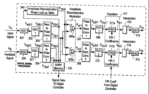
Figure 3 is a block diagram of one embodiment of the digital signal
processor 101B of the multicarrier driver assembly 101. Figures 4A-4D
illustrate
additional detail of the frequency plan, incorporated into the digital signal
processor.
Referring to Figure 3, the input signal V;" is converted by analog-to-digital
converter (ADC) 301. The output of ADC 301 is coupled to the inputs of digital
downconverter (DDC) 302, which translates the signal frequency (75 of Figure
4A) by one quarter of the ADC sample rate (i.e., Fs/4) to baseband (76 of
Figure
4B), using a complex frequency translation. DDC 302 also filters this signal
to
remove the undesired harmonic component at Fs/2 (77 of Figure 4B) to achieve
the frequency plan of Figure 4C. Thus, DDC 302 converts sampled real signals
into complex baseband signals. The output of DDC 302 comprises an in-phase
(I) component and a quadrature-phase (Q) component. Figure 4D shows the
resulting signal spectrum. Note that in one embodiment, the output samples
could be decimated or interpolated by any factor.
The output of DDC 302 is input into the remainder of Figure 3 which
represents one exemplary embodiment of a linearizer that takes the input
signal
and converts it to a number of signals that are applied to amplifier modules
1021.
N in the bank of existing amplifiers. In other words, the linearizer prepares
a
multicarrier input signal for processing by amplifiers. The amplifiers may be
those amplifiers of an existing base station.
This linearizer may include input equalizers (not shown) that equalize
amplitude and phase variations that exist and which are common to all
channels.
In one embodiment, these input equalizers comprise a finite impulse response
12
CA 02362101 2001-08-03
WO 00/46916 PCT/US00/02586
(FIR) filter that utilizes equalizer filter coefficients in a manner well-
known in
the art.
Rectangular to polar (R2P) converter 304 converts the rectangular
coordinate in-phase (I) and quadrature-phase (Q) input to polar coordinate
amplitude and phase format with amplitude and phase components. The phase
component represents the angle modulation component of the input signal
while the amplitude component represents the envelope modulation component
of the input signal.
The phase component is coupled to the input of amplitude reconstruction
modulator 305. Amplitude reconstruction modulator 305 is also coupled to
receive inputs from amplitude reconstruction phase modulation generation
module 340. In one embodiment, the amplitude reconstruction phase
modulation generation module 340 comprises an amplitude reconstruction
phase look-up table that generates a Pmod signal.
In one embodiment, amplitude reconstruction phase modulation
generation module 340 generates Pm~ in response to the amplitude of the input
signal output from R2P 304, referred to as Ar2P, according to the following:
Pm~ = arccos(A)
where A = min(AizP/Elef,1). The value Eref is a predefined reference
magnitude.
In one embodiment, Elef is the clip value. The operation of the amplitude
reconstruction phase modulation generation module 340 provides phase values
for setting the angle between the two summing vectors after the amplification.
This is used to reconstruct the required amplitude values of the amplitude
modulated input signal.
In one embodiment, amplitude reconstruction module 305 supplies the
phase modulation Pmod to adders 305A and 305B contained therein. Note that
P~,~ is added with adder 305A, while Pmod is subtracted with adder 305B. In
other
words, the amplitude reconstruction modulation comprises a set of phase
13
CA 02362101 2001-08-03
WO 00/46916 PCT/US00/02586
modulation signals, Pa~, and Part, one for each output channel, and these
signals
are defined as follows:
Parl = Pr2p1 + Pmod
Pare = Pr2PZ - P~"~
The net result is to combine two constant amplitude vectors and reconstruct
the
amplitude modulation present on the input signal.
The phase modulation signals Pa~, and Pare are coupled to a pair of polar to
rectangular (P2R) converters 307 and 308. P2R converters 307 and 308 convert
the polar coordinate amplitude and phase input signals (the amplifier channel
signals) into rectangular in-phase (I) and quadrature-phase (Q) signals.
The outputs of P2R converters 307 and 308 are coupled to a pair of digital
upconverters (DUCs) 309 and 310 located in each transmit channel. 'The
transmit
I and Q signals for each transmit channel are converted from complex baseband
signals to real signals and interpolated by DUCs 309 and 310.
The outputs of DUCs 309 and 310 are coupled to a pair of equalizers 311,
which equalize amplitude and phase variations that may exist. In one
embodiment, equalizers 311 comprise FIR filters 311a and 311b that operate
using equalizer coefficients generated in the manner described below.
The outputs of equalizer 311 are coupled to two interpolators 315 and 316.
The outputs of interpolators 315 and 316 are coupled to digital-to-analog
converters (DAC) 312 and 313, respectively, which convert the digital signals
to
analog format. These outputs drive the amplifier channels.
Buffer memory 330 stores synchronously captured consecutive samples
from both the input channel (V;") and the feedback channel (V~). Buffer memory
330 maintains an association of the samples downloaded to digital controller
110
for use thereby.
ADC 320 and digital downconverter 321 are included to process the
feedback signal V,~ to produce a sampled feedback signal.
14
CA 02362101 2001-08-03
WO 00/46916 PCT/US00/02586
Figures 5A-D illustrate a frequency plan for frequency conversion
contained within the transmit channels. Figure 5A shows the frequency plan
present at the inputs of DUCs 309 and 310. In one embodiment, DUCs 309 and
310 first interpolate their input signals by inserting zeros between samples
to
increase the sample rate and then filter their input signals to remove the
component at the new Fs/2 where Fs is the new sample rate. Figure 5B
illustrates the frequency plan after half-band filtering. Finally, the signal
is
quarter-band up-shifted (i.e., Fs/4). Figure 5C illustrates the frequency plan
after the quarter-band (Fs/4) up-shifting and selection of only the real part
of the
signal to produce the desired spectrum. Figure 5D illustrates the frequency
plan
at the D/A output after interpolating by 2 on the input. In an alternative
embodiment, polyphase filters are used to further increase the sample rate by
interpolation.
It should be noted that some of the digital signal processing operations
described herein may be performed in software, hardware, or a combination of
the two. Such software may be run on, for example, a dedicated or general
purpose machine, such as a computer system, while the hardware may
comprise, for example, dedicated logic, circuits, etc. Also, although the
above
describes an embodiment that performs digital processing in the polar
coordinate domain, the processing could be performed in the I and Q
(rectangular coordinate) domain.
Calibration Procedure
A model of a linear amplifier based on the principle of amplitude
reconstruction is shown in simplified form in Figure 6. Note that the
individual
amplifiers are not necessarily linear; however, by performing this type of
CA 02362101 2001-08-03
WO 00/46916 PCT/US00/02586
reconstruction, the nonlinear effects on the signal amplitude can be
substantially
reduced and even minimized.
Referring to Figure 6, an input signal u(n) is coupled to the input of
nonlinear function F(u). The nonlinear function F(u) converts the amplitude
modulated signal u(n) to N phase modulated signals with constant amplitude.
In one embodiment, N is 2. The outputs of the nonlinear function F(u) (defined
below) are coupled to a pair of equalizers h, and h2. In one embodiment, the
equalizers hl and hZ are a pair of finite impulse response (FIR) filters. The
outputs of equalizers hl and hz are coupled to power amplifiers gl and gZ. In
one
embodiment, power amplifiers g1 and g2 also include filters, RF upconverters
(including RF filters), digital-to-analog converters (DACs), and isolators.
The
outputs of power amplifiers g1 and g2 are coupled to inputs of a summation
block, the output y(n) of which is the output of the linear amplifier. In one
embodiment, the function summation block comprises power combiner 103
described above. Note that although not shown, in one embodiment, there are
isolators in each path, along with IF and RF filters.
Although Figure 6 is described with two channels, a decomposition by
the non-linear function F(u) may be into N amplitude reconstruction channels.
In such a case, the amplifier model will have g,, g2, ... and the equalizer
will have
h,, h2, ....,hN.
The input signal u(n) is applied to the nonlinear function F(u). The input
signal u(n) is a complex baseband input signal u(n) = a(n) exp(j b(n)) with
16
CA 02362101 2001-08-03
WO 00/46916 PCT/US00/02586
amplitude a(n) and phase modulation b(n). In one embodiment, the amplitude
a(n) is clipped based on its magnitude. In one embodiment, the clipped
amplitude function a (n) is as follows:
a(n), a(n)< A~~p
a(n)= h a(n) >_ A .
~<<p
where Aclip is a predefined clip level which is dependent on the system
hardware. In one embodiment, the clip level is 0.7821.
In response to the input signal u(n), the non-linear function F(u) produces
a pair of frequency modulated signals xl(n) and x2(n). The pair of frequency
modulated signals xl(n) and x2(n) are given by
xl(n) - eJ(b(n)+c(n))
x2(n) = eJ(b(n)-c(n))
where:
c(n) = cos ' ( a (n)) .
The resulting signals x1(n) and x2(n) are processed by equalizers hl and h2
and power amplifiers ggl and gg2. The output of the amplifiers, referred to
herein as wg, (n) and wB~ (n), are summed to generate the output y(n).
If the equalizers h1 and hZ and power amplifiers gl and g2 in each channel
provide constant gain G, then it can be shown that the output y(n) is exactly
equal to a scaled and clipped version of u(n). That is, the amplifier acts as
an
17
CA 02362101 2001-08-03
WO 00/46916 PCT/US00/02586
ideal soft-limiting amplifier. If the clip level is not exceeded, then the
equivalence is exact. This is shown in the derivation below.
y (n) = wg~ (n) + wg2 (n)
= GLej(b(n)+c(n)) + ej(b(n)-c(n)) 1
= Gej(b(n)) LeJ(c(n)) + ej(-c(n))
= 2Gej(b(n)) cos(c(n))
= 2Gej(b(")) cos(cos-' (a(n))
= 2Ga(n)ej(b(n))
2Ga(n)ej(b(n))
Unfortunately, amplifiers g1 and g2 are rarely equal to a frequency
independent constant gain G as assumed above. Any differences in the two
channels (upper and lower paths) and/or frequency response variations can
cause distortion products to appear in the output y(n). In addition, in one
embodiment, amplifiers g1 and g2 have the nonlinear characteristic of high-
power amplifiers. This latter effect is somewhat mitigated by the fact that
amplitude reconstruction relies on constant amplitude signals passing through
the high-power stages (i.e., gl and g2) and consequently the effects of the
nonlinearities are generally slight. Equalizers hl and h2 provide the
necessary
gain, phase and frequency response corrections necessary to balance the two
channels, and the attempt to compensate for the nonlinearities and minimize
distortion. In one embodiment, equalizers hl and h2 are implemented as FIR
filters that can, in principle, provide both gain and phase balance as well as
compensate for the frequency response of each channel separately.
18
CA 02362101 2001-08-03
WO 00/46916 PCT/US00/02586
The overall goal is to make the frequency response of each channel equal
to each other and to be as flat as possible over the band of interest (in that
there
are no dips or spikes or sharp cut-offs, or these are reduced or minimized
with
respect to each other). This is accomplished by use of adaptive equalizers in
an
adaptive system that implements two major functions: i) estimation of the
amplifier transfer functions (referred to herein as system identification),
yielding
a linear amplifer system model; and ii) computation of the equalizer
coefficients
using the amplifier model (referred to herein as adaptive equalization). Also,
constraints are used so that the frequency response of each channel is
approximtely flat. This may be accomplished in two ways: 1) a least squares
constraint for each channel, and 2) a zero-forcing constraint for each
channel.
The degree to which a constraint contributes to the overall reduction or
minimization is controlled by two user-adjustable promoters, y, greater than
or
equal to 0 and y2 greater than or equal to 0, where ~y, + y2 = 1.
In contrast to the prior art, the equalization is performed before the
amplifier (i.e., pre-equalization). In one embodiment, the equalization is
performed in the digital domain before amplification, whereas the
amplification
is performed in analog. In other words, the purpose of the equalization is to
time align, phase align, and magnitude align the signals from the two channels
so that an amplified version of the original input signal to the amplifier may
be
obtained from the summation of the two channels. Also, as described above, in
one embodiment, the equalization is performed on the phase component of the
19
CA 02362101 2001-08-03
WO 00/46916 PCT/US00/02586
amplifier configuration, apart from the amplitude, which is different than the
prior art.
A System Identification Process
A calibration scheme based on the principle of linear least squares is
shown in Figure 7. Referring to Figure 7, actual amplifier 600 shown in Figure
6
is coupled to a amplifier model 700 having a nonlinear processing function
F(u),
a pair of equalizers h, and h2, amplifier models g , and g 2 (vectors), and a
summation block. The nonlinear function F(u) and equalizers hl and hz in
amplifier model 700 are identical to those in amplifiers 600. However,
amplifier
models g , and g 2 (vectors), are only estimates of the actual amplifiers g,
and gz.
The actual amplifiers contain nonlinear components that cannot be modeled the
FIR filters, and even the linear components may not be sufficiently modeled if
the FIR filters do not have enough parameters. This difference may affect the
performance of the equalizers because they are generated from the amplifier
models, i.e., h, and hZ attempt to invert the characteristics of g , and g z
(vectors),
(and not g, and gz, which are not directly available). Note that some vectors
appear in bold.
The nonlinear function F(u) of amplifier model 700 is coupled to receive
the same input signal u(n) as actual amplifier 600. A system identification
block
701 is coupled to receive the output signal y(n) of actual amplifier 600, the
output signal y g(n) of amplifier model 700, and the input signal u(n). In one
embodiment, system identification block 701 is part of digital controller 110.
In
response to these signals, system identification block 701 generates outputs
(not
shown) to the equalizers of both actual amplifier 600 and amplifier model 700,
the nonlinear function F(u) of actual amplifier 600, and the amplifiers of
amplifier mocel 700.
CA 02362101 2001-08-03
WO 00/46916 PCT/US00/02586
Although not shown in Figure 7, buffers receive samples of the input
signal u(n) and capture samples of the outputs of both actual amplifier 600
and
amplifier model 700. System identification block 701 accesses these buffers to
obtain samples when performing one or more of its functions.
A goal of this least squares technique is to compute equalizers hl and hz
such that the actual output y(n) matches a delayed version of the input u(n)
in
the least squares sense (as defined below). In order to achieve this goal, the
amplifier models g 1 and g 2 are estimated such that y(n) matches y(n), also
in
the least square sense.
Normally, when the equalizers are located ahead of the amplifiers (as in
this case), it is difficult to directly compute the least squares estimates
because
the amplifier characteristics are unknown. The gradient from y(n) to each of
the
equalizer input signals, x,(n) and xz(n), is needed to compute the least
squares
estimates, but this requires knowledge of the amplifiers. This problem is
circumvented by computing a reference model of the amplifiers whereby the
actual amplifiers g, and g2 are estimated by linear filters g , and g 2
(vectors).
As mentioned above, the amplifier models and the equalizers may be
represented by FIR filters. Therefore, the transfer functions of the amplifier
models may be written as follows:
N~-1
Gnz)- ~g (i)z-'
-o
Ng -1
GZ(z)- ~gz(i)z '
-o
where Ng is the number of coefficients in each channel of the model.
Similarly,
equalizer may be represented as follows:
21
CA 02362101 2001-08-03
WO 00/46916 PCT/US00/02586
Ne _1
Huz)= ~h~, az_;
r=o
N 1
Hz(Z)_ ~hz~ Z r
=o
where Ne is the number of coefficients in each equalizer. Typically, Ng>_Ne
because Ne is restricted by the hardware, whereas Ng can be somewhat arbitrary
because it is implemented by the controller. In one embodiment, Ng=32 and
Ne 16, although it is desirable that they be as small as possible.
Referring to Figure 7, the equalizer outputs referred to as vg,(n) and vgZ(n)
are given by:
vg,(n)=h,(n)~x,(n)
N -1
_ ~ h~, axe (n - l~ = x~ (n )h~
r=o
vAZ(n) = hz(n)*xz(n)
N -1
_ ~hz,axz(n -l)= xz(n)hz
r=o
where x,(n) _ [x,(n),..., x,(n - Ne + 1)] T , x2 (n) _ [x2 (n),...,xz(n- Ne +
1)] T ,
hl = [h,,l~~~~~hl,e-,] T ~ hz - [hz,l~"'ihz,Ne-1] T , and *denotes
convolution. These can
replaced by vector inner products to simplify the notation.
Computing the Amplifier Models
To compute the amplifer models, let u(n) _ [u(n), u(n-1), . . ., u(n-NS+15)]T
be a vector of the size NS containing the n-th block of samples of the input
signal
u(n). Similarly, define vectors y(n), vg,(n), vgz(n), w gl(n), w g2(n) and y
g(n), where
the vector y(n) comprises the output of actual amplifier 900, the vectors
vg,(n)
22
CA 02362101 2001-08-03
WO 00/46916 PCT/US00/02586
and vgZ(n) are the outputs of the equalizers of either actual amplifier 600 or
amplifier model 700, the vectors vg,(n) and vgz(n) are the first and second
channel
amplifier model signals of amplifier model 700, respectively, and the vector
y g(n) is the output of amplifier model 700.
The amplifier model signals wl(n) and w Z(n) can be expressed in
matrix/vector notation as follows:
~'g ~ (n ) = Vg, (n)g~
~'~'gz ( n) = Vgz ( n)gz
where Vg,(n) and Vgz(n) are Toeplitz matrices formed using the signal vectors
vg,(n) and vgz(n). These matrices may be represented as follows and are only
one
of many possible ways to store the data for this technique.
wg~(n) o of
I vgl (n _ 1 ) vg un) I
~~~ (k) =
I V~, (n o S + 1 ) I
L~ J
rvgl(n) 0 0~
I vgz(n_1) vgZ(n) I
Vgz(n)-I I
I vgz (n-N +1) I
0
J
Note that Vg,(n) and Vg2(n) correspond to the first columns of these matrices,
respectively (though zeros have been appended so that the dimensions of the
matrices are ((NS + Ng) x Ng). The output of the amplifier model is given by
the
following:
23
CA 02362101 2001-08-03
WO 00/46916 PCT/US00/02586
yg (n) = wg~ (n) + wRZ (n )
Since the amplifier model in both channels will be estimated simultaneously,
it
will be convenienct (and more compact) to define the compound coefficient
vector g (vector) _ [gi , g2 JT and the compound data matrix Vg(u) _
[ V g (n), Vg2 (n) J. Thus, the equation for the output of the amplifier model
can be
rewritten as:
Yg (n) = ws ~ (n) + ~'xz (n )
= VR~(n)gW' VR2(n)gz
_ ~Vg~(n)~ V~2(n)
g2 J
=1'g(n)g
with Vg,(n) representing the output of one of the two equalizers and Vg2(n)
representing the other, and Vg(n) representing all of the data for the output
of
the equalizer. Thus, by this representation, the output of amplifier model 700
is
written in terms of the outputs of the equalizers and the amplifier transfer
functions.
Let the cost function associated with estimating g 1 and g 2 (vectors)
C1 m)=al YCn-PI)- yg (n - P2 ) 112
where p, and pz are delays introduced by the actual amplifiers and the model
amplifiers, respectively. For convenience, these are ignored in the
derivations
below. It is important, however, that they be chosen correctly so that the
algorithm will function properly. Note that IIbIl2 = bTb corresponds to the
norm
24
CA 02362101 2001-08-03
WO 00/46916 PCT/US00/02586
squared of the vector b . The real-valued parameter a, compensates for any
gain mismatch at the output.
Substituting the output of the model amplifiers for y g(n) (vector) (and
suppressing p, and p2 ) yields
Cl(n=Ilal yy) - Vgy)g 2
= C al YTCn) - gT Vg (n)Ilal Y(n) - Vg(n)g~
Differentiating with respect to g (vector) yields
7C, (n) _ _2a, VR (n)y(n) + 2V~ (n)g
ag
Solving aC, (n ) l r7g = 0 for g (vector) gives the LS result
g[V~ (n)Vg(n)j'[a~V~ (n)y(n),
~'(n)P~(n)
This expression can be rewritten in terms of the individual coefficient
vectors as
follows:
g, _ Vx (n)Vgt(n) Vg (n)Vgz(n) ~ a~VB (kpOn)
LSz] [Vg (n)V8~(n) Vg (n)VKZ(n)1 [a~VBZ(k)y(n)~
In practice, a matrix would not be inverted directly as in the expressions
above.
Instead, Gaussian elimination (GE) (or another efficient method) would be
employed to solve the following set of equations:
~Vg (n)Vg (n)~ g = ~a, V~ (n)y(n)~
CA 02362101 2001-08-03
WO 00/46916 PCT/US00/02586
Note that the matrix on the left-hand side of the equation above is not
Toeplitz
(though it is symmetric). Since it is only block Toeplitz, as is evident from
the
right-hand side of the expression of the LS result (written in terms of
individual
coefficient vectors), it may not be possible to use a Levinson-type recursion
(instead of GE) to solve for g (vector). (For an N x N matrix, GE requires
o(NZ )
operations, whereas the Levinson algorithm reduces this to o(N) .)
Enhanced Edualizer Process
The equalizers h, and h2 are computed in a manner similar to that used to
generate the amplifier models g , and g z. A block diagram of the system
configuration is shown in Figure 8. Comparing this system with the model in
Figure 7, observe that the equalizers and the amplifier models are transposed.
This can be done without loss of generality because the systems are linear.
The
input signals X,(n) and x2(n) are generated as before, but the intermediate
signals following the models and the equalizers are different from before
because of this interchange. This change is emphasized by using different
notation: ~h,(n) and ~h2(n) are the output signals of the amplifier models,
whereas wh,(n) and w,,2(n) are the output signals of the adaptive equalizers
The new cost function for the adaptive equalizer is
CZ(n) = Y~C2~ (n) +~1- YO~YZ~Czz (n)+ Cz3(n)~+ (1- YaJlCza +' Czs)
where the individual components are given by
C2~(n)=~~az~u(n-P3)-Yh(n-PZ) 2
Czz(n)= a2zX(n-P3)-~'h(n-Pz)II
26
CA 02362101 2001-08-03
WO 00/46916 PCT/US00/02586
z
Cz4 -Ila'zal-Gihyl
Cz5 =Ila'zsl-Gzhzllz
where 1 is a unit vector; the location of the one depends on the system
delays.
C2, (n) is one embodiment of the cost function for the equalization;
minimizing
C2, (n) alone will yield equalizers such that yh(n) approximates u(n) in the
LS
sense. c22(n) and cz3(n) are LS constraints for each channel separately; these
adjust the equalizers so that the intermediate output signals wh,(n) and
wh2(n)
approximate the input signals x, (n) and XZ (n) , respectively. Finally, CZ4
and CZs
are zero-forcing constraints; these adjust the equalizers such that h;(n)
convolved with g(n) ( i = ~,2 ) yields a (Kronecker) delta function, i.e.,
h~ Vin) * g~ ~n)=a2,s~n -P4)
The model amplifier delay is pz (the same as before), p3 is the delay from the
input u(n) to X,(n) (and XZ(n) ), and p4 is the effective (group) delay of the
left-
hand side of (1). (Note that all the p; , i =1, 2, 3, 4 refer back to the
input u(n) .)
For convenience, the delays are suppressed in the derivations below. The a;~
are
scalar constants included to compensate for any gain mismatches among the
signals in the cost function terms. The weighting coefficients y, and yz were
described previously.
Using matrix/vector notation, the output in terms of the equalizer
coefficients h, and h2 may be written as follows:
27
CA 02362101 2001-08-03
WO 00/46916 PCT/US00/02586
yn (n) = wn~ (n) + wnz (n)
= V n~ ( n)~ + Vn2 (n )hz
_ ~Vn~(n)~vn2(n)~hz
= Vn(n)h
where wh,(n) and w,~(n) are the output signal vectors of the equalizers and
rvhl(n) 0 0~
i ~h~(n-1) °hl(n)
Vn~ (n) _
Vn, (n -1V5. + 1 )
0
J
i "hz (n) 0 0 i
vhz(n-1) ~'hz(n)
vn2(n)-
vn2(n-N~+1)
0
J
which are similar in form to Vgl(n) and Vgz(n) matrices given above.
Original Cost Function
Consider the component c2, (n) , which is the cost function of the original
algorithm. Substituting the output in terms of the equalizer coefficients h,
and h2
into the cost function c2, (n)
C (n) Ila u(n) V (n)hli2
21 21 h
_ [oc21 uT (n) - hT Vh (n)yoc2lu(n) - V(n)h
Differentiating with respect to h yields
28
CA 02362101 2001-08-03
WO 00/46916 PCT/US00/02586
a~,(n)--2V,,(n)u(n)+2Vh (n)Vh(n)h
ah
Solving ace, (1,) / ah = o gives the following (partial) LS solution for the
equalizer
coefficients:
~Vn (n)Vh (n))h = La2luh (n)u(n)~
which we will represent by
R2~ (n)h = Pz1 (n)
As was done for the amplifier models, the partial LS solution can be written
in
terms of the two channel coefficient vectors separately, as follows:
VhIT(n)Vhl~n)uhi(n)Vh2(n) hl a,21vh1(")°(")
Vh2(n)uh1(n)uh2(n)uh2(°) J h2 a21uh2(n)°(")
Least-Sguares Constraints
For the cost function in C2, (a) given above, it can be written
Czz(n) _ ~~a22X1(n)-~'m(n)hl~I2
Similarly, for CZ, (n) given above, it can be written
C23 (n) - IIa23x2 (n ) - V,,z(n)h2112
It is clear from the result in the (partial) LS solution for the equalizer
coefficients
that C23(n) and C24(n) given above are minimized, respectively, by
LV , (n)V n ~ (n) ~ h , _ [a zz V > , (n)x 1 (n)
~V n z (n)V n z (n) ~ h 2 = [a z3 V n z (n)X (n) ,
2
29
CA 02362101 2001-08-03
WO 00/46916 PCT/US00/02586
Observe that the components on the left-hand side of these expressions
correspond to the diagonal components on the left-hand side of the LS solution
for the equalizer coefficients (written in terms of two channel coefficient
vectors).
Thus, the equations above may be combined in a similar manner, yielding the
partial LS solution
Vn (n)Vm (n) 0 h' _ azzVn (n)X~ (n)
0 Vh (n)Vnz(n) h2 az3V 2(n)X'-(n)
which will be represented by
Rzz (n)h = PZZ (n)
Note that u(n) in the (partial) LS solution is replaced by x,(n) and XZ(n) in
the
equation for the LS solution given above. Recall that C22(n) and Cz3(n) are
weighted by the same coefficient (~-y,>y2.
Zero-Forcing Constraints
The two remaining cost functions, Cz4 and C25, are zero-forcing constraints;
the equalizers are computed so that the combined equalizer/system model 700
yields a delta function as discussed previously. The cost functions in Cz4 and
c25 given above are not written as functions of n to emphasize that they do
not
depend directly on the data like the other cost functions. Using the
previously
used notation, the partial LS solutions may be written as follows:
T T
~Gi Gu hi - a2aGi 1
~G~ G~ ~ h2 = a Gi 1
30
CA 02362101 2001-08-03
WO 00/46916 PCT/US00/02586
where
~ 8~,~ 0 0 ~
G~ _ I gi, z g~
~ g~0 g
J
r~
~ g2,, 0 0 ~
GZ _ ~ g2.2 g2,1
J
and 1T =(o,...,o,l,o,...,o); the location of the one in this vector is
specified by the
delays of the equalizer and the system model 700. Combining the terms in
yields the following expression:
~G~ G, ~ h, = a,24G;1
~GZG2~ h2 = a25Gz 1
which can be represented as
R Zsh = Pzs
Note that both zero-forcing constraints are weighted by ( t - y, )( 1- y2 ) .
Enhanced Equalizer Coefficients
At this point, the partial LS solutions has been specified for the original
set of
individual cost functions given above. Thus, combining the results in with the
31
CA 02362101 2001-08-03
WO 00/46916 PCT/US00/02586
appropriate weighting of y, and y2, the optimal equalizer coefficients are
computed by solving the following linear system of equations:
~Y~R2On)+WY~)Y2R22O)+WYi)WYz)R2s~h=
~YiP2On)+WYi)YzPzzO)+~1-Y~)~1-Yz)Pz3~
Recall that the gain coefficients a;~ are embedded in the P;~ (cross-
correlation)
vectors. By varying the weightings y; , how much the solution depends on the
original cost function versus the new cost functions (constraints) defined
separately for each channel may be controlled. There are three special cases:
1) Original LS Equalizer: y, =1: RZ, (n)h = P2, (n)
2) Separate LS Equalizers: y, = o and y2 =1: R 22 (n)h = Pzz (n)
3) Zero-Forcing Equalizers: y, = o and y2 = o : R 23h = Pzs
Calibration Procedure Flow
One embodiment of the calibration procedure is shown in Figure 9. In
one embodiment, the calibration procedure is performed by deducted
processing hardware. This processing hardware may comprise hardware, such
as, for example, digital or analog circuitry or, software, such as, for
example, that
which runs on a general purpose or dedicated machine, or a combination of both
hardware and software. In one embodiment, the processing logic comprises
controller 1101.
Referring to Figure 9, the calibration procedure begins by processing logic
obtaining the current equalizer values (processing block 1301). The current
equalizer values comprise normalized equalizer FIR tap values for each
channel.
32
CA 02362101 2001-08-03
WO 00/46916 PCT/US00/02586
In one embodiment, separate matrices of the current equalizer values are
maintained. In an alternate embodiment, a single matrix may be used instead of
the two matrices. In still another embodiment, the values may be stored in
registers or any other type of memory.
Next, processing logic obtains the capture buffer data and reformats the
data to a normalized signal format (processing block 1302). If the data are
captured in a normalized signal format, then the reformatting is not
necessary.
In one embodiment, four thousand samples are stored in the capture buffer
(e.g., buffer memory 330). The capture buffer stores the samples in a matrix
form.
After capturing the buffer data and performing reformatting, processing
logic decomposes the input signal into an amplitude reconstruction channel
pair
(processing block 1303). In one embodiment, the results of the decomposition
produces the baseband waveforms for both channels (x,(n) and x2(n)) as well as
the baseband waveforms after the equalizer.
With the decomposition complete, processing logic estimates the model
FIR coefficient (tap) values for each channel (processing block 1304). As
discussed above, these are the g 1 and g z, values. The FIR tap values attempt
to
make the two or "N" amplitude reconstruction channels all alike. In one
embodiment, the processing logic estimates the model FIR coefficients using
the
baseband waveforms after the equalizer and the delays of actual amplifier 600
and amplifier model 700.
33
CA 02362101 2001-08-03
WO 00/46916 PCT/US00/02586
Using the baseband waveforms, processing logic recomputes the
amplitude reconstruction channel pair (processing block 1306). This channel
pair comprises the baseband waveforms that appear at the output of the
equalizer.
Using the amplitude reconstruction waveforms that appear at the output
of the amplifiers for both channels and the output of the combiner, processing
logic computes new equalizer FIR tap values using the model FIR tap values for
both channels (processing block 1307).
Lastly, processing logic converts and writes the new equalizer FIR tap
values into hardware registers (processing block 1308). The hardware registers
are accessed by actual amplifier 600 to linearize itself as described above.
Therefore, embodiments described herein provide high power
amplification of signal or multiple RF carriers with low intermodulation
distortion within a cellular AMPS base station using the existing AMPS single
carrier amplifiers.
Such embodiments may provide linear amplification for CDMA and GSM
carriers or other digital carriers. The linear application uses the precision
of
digital signal processors and provides the linear amplification in the digital
domain without any critical periodic tuning or alignment. In this manner,
embodiments) described herein provide amplification of one or more than RF
carriers and transmits them from an antenna using saturated or nearly
saturated
amplifiers.
34
CA 02362101 2001-08-03
WO 00/46916 PCT/US00/02586
The linearization described herein may be applied to audio frequency
amplifiers as well.
Thus, a technique is described for multi-carrier signal amplification for
wireless base stations where multiple saturated or nearly saturated amplifiers
are used to implement a linear amplifier. With one embodiment, other protocols
such as, for example, CDMA, can be superimposed on a base station, such as an
AMPS base station.
Whereas many alterations and modifications of the present invention will
no doubt become apparent to a person of ordinary skill in the art after having
read the foregoing description, it is to be understood that any particular
embodiment shown and described by way of illustration is in no way intended
to be considered limiting. Many other variations are possible. For example,
the
amplifier may be a single amplifier or multiple amplifiers as described or may
comprise a number of amplifiers configured to act as a single amplifier. The
application may be that of cellular, PCS, or any other frequency range that
one
may consider. It can be used for wireless local loops, smart antennas, audio
amplifiers, or radar applications. Therefore, references to details of various
embodiments are not intended to limit the scope of the claims which in
themselves recite only those features regarded as essential to the invention.
Thus, a linear amplification technique has been described.