Note: Descriptions are shown in the official language in which they were submitted.
CA 02362216 2001-11-14
ENHANCING ADHESION OF ORGANIC ELECTROSTATOGRAPHIC IMAGING
MEMBER OVERCOAT AND ANTICURL BACKING LAYERS
BACKGROUND OF THE INVENTION
Field of Invention
This invention relates in general to an electrostatographic imaging member,
and in particular, to a process for preparing electrostatographic imaging
members and
to imaging members produced thereby. In particular, the invention provides a
process
for enhancing the adhesion of an overcoat layer to the top outermost organic
layer of
an organic electrostatographic imaging member. Since organic
electrostatographic
imaging members in a flexible belt configuration require an anticurl backing
layer to
ensure that the imaging member belt is sufficiently flat, the process of the
present
invention can also provide improved adhesive bond strength between an anticurl
backing layer and a substrate support layer.
2. Description of Related Art
Electrostatographic imaging members are well known in the art. Typical
electrostatographic imaging members include, for example, ( 1 ) photosensitive
members (photoreceptors) commonly used in electrophotographic (xerographic)
imaging processes and (2) electroreceptors such as ionographic imaging members
for
electrographic imaging systems. An electrostatographic imaging member can be
in a
rigid drum configuration or in a flexible belt configuration, that can be
either a
seamless or a seamed belt. Typical electrophotographic imaging member drums
comprise a charge transport layer and a charge generating layer coated over a
rigid
conducting substrate support drum. However, for flexible electrophotographic
imaging member belts, the charge transport layer and charge generating layer
are
coated on top of a flexible substrate support layer. To ensure that the
imaging
member belts exhibit sufficient flatness, an anticurl backing layer is coated
onto the
back side of the flexible substrate support layer to counteract upward curling
and
ensure imaging member flatness.
A typical flexible electrographic imaging member belt comprises a dielectric
imaging layer on one side of the substrate support layer and an anticurl
backing layer
coated onto the opposite side of the substrate support layer to maintain
imaging
member flatness.
CA 02362216 2001-11-14
2
The top outermost layer, typically the charge transport layer of an
electrophotographic imaging member or the dielectric imaging layer of an
electrographic imaging member, is constantly subjected to mechanical and
chemical
actions with machine subsystems during imaging/cleaning processes. In order to
mitigate erosion of the top outermost layer during these processes, the
outermost layer
can be coated with a thin protective overcoat to provide wear resistance and
extend
the imaging member's functional life. Although the present invention applies
to both
electrophotographic and electrographic imaging members, to simplify the
following
discussion, the discussion hereinafter will focus only on electrophotographic
imaging
members, particularly, imaging members in the flexible belt configuration.
In electrophotography, also known as Xerography, including
electrophotographic imaging or electrostatic imaging processes, the surface of
an
electrophotographic imaging member (or photoreceptor) containing a
photoconductive
insulating layer on a conductive layer is first uniformly electrostatically
charged. The
imaging member is then exposed to a pattern of activating electromagnetic
radiation,
such as light. The radiation selectively dissipates the charge on the
illuminated areas
of the photoconductive insulating layer while leaving behind an electrostatic
latent
image. This electrostatic latent image can then be developed to form a visible
image
by depositing oppositely charged particles on the surface of the
photoconductive
insulating layer. The resulting visible image can then be transferred from the
imaging
member directly or indirectly (such as by a transfer or other member) to a
print
substrate, such as a transparency or paper. The image process can be repeated
many
times with reusable imaging members.
Flexible electrophotographic imaging members can be provided in a number
of forms. For example, the imaging member can be a homogeneous layer of a
single
material, such as vitreous selenium, or it can be a composite layer containing
a
photoconductive layer and another material. In addition, the imaging member
can be
layered. Current layered organic imaging members generally have at least a
flexible
substrate support layer and two active layers. These active layers generally
include (1)
a charge generating layer containing a light absorbing material, and (2) a
charge
transport layer containing electron donor molecules. These layers can be in
any order,
and sometimes can be combined in a single or a mixed layer. The flexible
substrate
support layer can be formed of a conductive material. Alternatively, a
conductive
layer can be formed on top of a nonconductive flexible substrate support
layer.
CA 02362216 2005-O1-13
3
In many modem electrophotographic imaging systems the flexible
photoreceptor belts are repeatedly cycled to achieve high speed imaging. As a
result
of this repetitive cycling, the outermost organic layer of the photoreceptor
experiences
a high degree of frictional contact with other machine subsystem components
used to
clean and/or prepare the photorecptor for imaging during each cycle.
When repeatedly subjected to cyclic mechanical interactions against the
machine subsystem components, photoreceptor belts can experience severe
frictional
wear at the outermost organic photoreceptor layer surface that can greatly
reduce the
useful life of the photoreceptor. For instance, in printers that employ a bias
charging
roller or a bias transfer roller (BCR or BTR), frictional wear can be so
severe that the
outer exposed layer's thickness can be reduced by as much as 10 microns per
100,000
photoreceptor belt revolutions. Ultimately, the resulting wear impairs
photoreceptor
performance to such a degree that the photoreceptor must be replaced.
Replacement
of the.photoreceptor requires product downtime and costly maintenance.
Typically, manufacturers attempt to minimize frictional wear of the outermost
organic layer by applying a protective overcoating to the outermost layer with
various
materials including nylon materials, such as a crosslinked Luckamide overcoat,
so that
the photoreceptor is mechanically robust enough to reach a desired product
life goal.
Unfortunately, although Luckamide and similar materials can provide sufficient
protection against frictional wear, such overcoatings do not adhere well
enough to the
outermost layer of organic photoreceptors to sufficiently extend functional
life to
avoid the onset of premature overcoat delamination. For instance, although
nylon
overcoatings have been found to increase photoreceptor wear resistance and
increase
useful life by as much as four times, to achieve these advantages, it is
necessary to
heat the overcoat materials to an elevated temperature to bring about a cross-
linking
reaction to impart sufficient hardness and wear resistance. Although elevation
of
temperature to achieve total material cross-linking is needed to increase
overcoat
hardness and to enhance wear resistance, unfortunately, this cross-linking
process also
leads to poor adhesion between the overcoating and the top photoreceptor layer
on
which the overcoat is applied. As a result, the overcoating tends to
prematurely
delaminate, thereby negating the intended protective benefits of the
overcoating.
Various methods are generally known in the art to improve adhesion between
successive layers in a photoreceptor. For example, U.S. Patent No. 5,919,514
discloses
the use of plasma or corona discharge on an insulating member (substrate) of
CA 02362216 2001-11-14
4
a donor roll, to increase adhesion and to provide a uniform subsequent metal
coating.
The disclosed process includes the step of applying corona discharge to the
surface of
the donor roll, prior to coating the donor roll substrate with a photo or
thermally
sensitive composition comprised of a polymeric material and a conductive metal
nucleating agent.
Similarly, various methods such as plasma discharge and corona discharge are
known and used for various purposes. For example, U.S. Patent No. 5,635,327
discloses the use of glow discharge decomposition to apply amorphous silicon
containing at least one of hydrogen and a halogen onto a conductive substrate.
Likewise, U.S. Patent No. 5,514,507 discloses using plasma discharge to form a
layer
having amorphous silicon germanium as a main body containing at least
hydrogen,
fluorine and a Group III element.
Another problem commonly associated with flexible photoreceptor belts
during extended machine belt cycling is separation of the anticurl backing
layer.
Premature delamination of the anticurl backing layer from the photoreceptor
belt
substrate support layer, due to poor interfacial adhesion bond strength, can
often
reduce the belt's useful life by as much as 50%. Although various attempts to
eliminate premature delamination have been successful, for example U.S. Patent
No.
5,013,624, such measures are generally highly complex and require innovative
material reformulations.
Despite the above known methods for improving adhesion between
photoreceptor layers, there remains a demand for methods directed to improving
interfacial adhesion between a protective overcoating layer and the outermost
layer of
a photoreceptor onto which the overcoating layer is applied. Because of the
above
problems, there is an urgent need for effective methods of enhancing
interfacial
adhesion between overcoating materials and freshly coated outermost
photoreceptor
layers. There also remains a need for imaging members and photoreceptors
having
improved adhesion between an overcoating layer and an underlying layer, while
still
providing acceptable wear resistance to the imaging members and
photoreceptors.
Furthermore, there is also a need for a simple innovative approach, for
enhancing adhesive bond strength between an anticurl backing layer a substrate
support layer, that can be easily adapted and implemented in photoreceptor
belt
manufacturing.
SUMMARY OF THE INVENTION
CA 02362216 2002-02-13
The present invention is directed to a process for preparing an organic
electrophotographic imaging member, either in a flexible belt configuration or
in a
rigid drum configuration, having at least one charge generating layer and a
charge
transport layer, wherein the imaging member is added with an overcoating layer
S having increased interfacial adhesion bond strength between at least an
outermost
layer and the overcoating layer applied to the outermost layer. The process of
the
present invention comprises exposing the surface of the outermost organic
layer of the
imaging member to a corona effluent, and then immediately applying an overcoat
layer to the treated outermost layer. Since the corona discharge effluent
cleans as well
as activates the outermost surface, it increases the outermost layer's surface
energy to
improve overcoat solution wetting and can thereby enhances chemical bonding to
yield an increase in interfacial adhesion bond strength between the applied
overcoating and the treated outermost layer.
In particular, the present invention provides a process for preparing an
imaging member, comprising:
applying an organic layer to an imaging member substrate;
treating said organic layer with a corona effluent; and
applying an overcoating layer to said organic layer.
The present invention also provides imaging members formed by such a
process. Further, when applied to imaging members of the flexible belt
configuration,
the same corona effluent surface treatment process can be used to improve
adhesion
between an anticurl backing layer and an imaging member substrate support
layer
upon which the anticurl layer is applied.
It is, however, necessary to emphasize that the solvent or solvent mix system
used to prepare the applied coating solution should not dissolve the imaging
member
layer over which the coating solution is applied so that effective adhesion
enhancement can be achieved.
CA 02362216 2005-O1-13
Sa
According to an aspect of the present invention, there is provided a process
for
preparing an imaging member, comprising:
applying an organic layer to an imaging member substrate;
treating said organic layer with a corona effluent; and
applying an overcoating layer to said organic layer.
According to an aspect of the present invention, there is provided a process
for
enhancing adhesion of an overcoat layer to an organic layer of a
photoreceptor, the
process comprising:
treating a surface of an organic layer of an organic photoreceptor with
a corona effluent; and
applying an overcoat layer to the surface of the organic layer.
According to a further aspect of the present invention, there is provided a
process for enhancing adhesion of an anticurl backing layer to a backside of a
flexible
substrate supporting layer of a photoreceptor belt comprising:
treating a backside of a flexible supporting layer of an organic
photoreceptor with a corona effluent; and
applying an anticurl backing layer to the treated backside of the
flexible supporting layer.
According to another aspect of the present invention, there is provided a
process for preparing an electrostatographic imaging member, the process
comprising:
a, applying an organic layer to an imaging member substrate;
b. placing the imaging member substrate, on which the organic layer
has been applied, in a first container;
c. generating a corona effluent by ionizing air with a corona discharge
device that is in a second container;
d. transferring the corona effluent from the corona discharge device to
the organic layer to surface treat the organic layer by directing a flow of
air through
the second container, thereby transferring the corona effluent from the second
container to the first container; and
e. applying an overcoating layer to the surface-treated organic layer to
form the electrostatographic imaging member.
According to a further aspect of the present invention, there is provided a
process for enhancing adhesion of an overcoat layer to an organic layer of a
photoreceptor, the process comprising:
CA 02362216 2005-O1-13
Sb
a. placing the photoreceptor in a first container;
b. generating a corona effluent by ionizing air with a corona discharge
device that is in a second container;
c. transferring the corona effluent from the corona discharge device to
the organic layer to surface treat the organic layer by directing a flow of
air through
the second container so that the corona effluent is transferred from the
second
container to the first container;
d, exposing the organic layer of the photoreceptor to the corona
effluent for a duration of time prior to applying the overcoat layer to the
organic layer;
and
e, applying the overcoat layer to the surface of the organic layer.
According to another aspect of the present invention, there is provided a
process for enhancing adhesion of an anticurl backing layer to a backside of a
flexible
substrate supporting layer of a photoreceptor belt comprising:
a. placing the photoreceptor belt in a first container;
b, generating a corona effluent by ionizing air with a corona discharge
device that is in a second container;
c. transferring the corona effluent from the corona discharge device to
the backside of the flexible supporting layer to surface treat the backside by
directing
a flow of air through the second container so that the corona effluent is
transferred
from the second container to the first container;
d. exposing the backside of the flexible supporting layer to the corona
effluent for a duration of time prior to applying the anticurl backing layer
to the
supporting layer; and
e, applying the anticurl backing layer to the treated backside of the
flexible supporting layer.
BRIEF DESCRIPTION OF THE DRAWINGS
Fig. 1 is a schematic view of an exemplary embodiment of a treatment system
according to this invention.
DETAILED DESCRIPTION OF PREFERRED EMBODIMENTS
CA 02362216 2005-O1-13
6
This invention is directed to a method for enhancing interfacial adhesion
between an overcoating layer and an underlying layer of an organic
photoreceptor by
treating the underlying layer with a corona effluent prior to applying the
overcoating
layer, and an organic photoreceptor prepared by such a method. Further, the
process
of the present invention is equally applicable to flexible organic
photoreceptor belts
that comprise anticurl backing layers.
Although overcoating organic photoreceptors with nylon materials, such as a
crasslinked Luckamide, is known to increase photoreceptor wear resistance and
product life by as much as four times, the temperature elevation needed to
initiate
cross-linking process in order to achieve these advantages has been found to
impair
interfacial adhesion between the resulting overcoating and the underlying
layer, such
as the charge transport layer. Poor interfacial adhesion between the
underlying layer
and the applied overcoating layer leads to premature delaminat3on of the
overcoating,
thereby minimizing the protective benefits of the overcoating. Moreover,
premature
anticurl backing layer delamination, often seen inflexible belt configured
photoreceptors during cyclic machine function, is also an issue that remains
to be
resolved.
According to embodiments of the present invention, an electrophotographic
imaging member is provided, that generally comprises at least a substrate
layer, a
charge generating layer, a charge transport layer, and an overcoating layer.
The
imaging member can be prepared by any of the various suitable techniques,
provided
that the outermost layer is treated by a corona effluent treatment method of
the present
invention, which will be described below, prior to applying the overcoating
layer. As
used herein, the term "outermost layer" refers to the outermost layer of the
photoreceptor design prior to application of an overcoating layer. Thus, while
the
outermost layer is not the final, exposed layer of the completed
photoreceptor, it is the
outermost layer of the incomplete photoreceptor prior to application of a
final
overcoating layer. The "outermost layer" thus likewise can be referred to as
an
underlying layer of the overcoating layer.
According to the present invention, the outermost surface of the
photoreceptor,
commonly the charge transport layer, is treated by corona discharge effluent
to prepare
the surface of the outermost layer. Rather than treating the outermost surface
of the
photoreceptor directly with a corona discharge, embodiments of the present
invention
CA 02362216 2005-O1-13
7
treat the outermost surface of the photoreceptor with a corona discharge
effluent.
Therefore, instead of roughening the surface of the outermost layer, as occurs
during
corona discharge treatment, embodiments of the present invention use corona
discharge effluents to increase surface energy for enhancing coating solution
wetting
as well as providing chemical activation of the outermost layer's surface,
through
cleaning the surface, and, possibly, also creating active sites on the surface
that can
enhance chemical bonding to the applied crasslinked overcoating layer. By
performing these functions, embodiments of the present invention can provide
increased interfacial adhesion between the outermost layer and a subsequently
applied
overcoating layer. In embodiments, such treatment can avoid the use of a
separate
adhesive layer between the outermost layer and the overcoating layer.
Preferably, the
treatment step of the present invention is conducted inline, as a step in the
production
process, that permits fabrication of an imaging member with increased
interfacial
adhesion between the photoreceptor's outermost layer and overcoating layer.
Preferably, in embodiments of the invention, the corona effluent treatment
only affects the outermost layer. That is, the treatment preferably physically
and/or
chemically alters only the outermost layer, such as by cleaning the surface of
the layer
to obtain an ultra clean outermost layer surface to promote overcoating
solution
wetting and intimate contact between the outermost layer and the applied
overcoating
layer: Moreover, such treatment ca.n also enhance chemical bonding between the
surface of the outermost layer and the applied overcoating layer so that the
adhesion
between the outermost layer and the overcoat are further enhanced.
According to the present invention, the specific parameters of the treatment
step will generally depend upon, for example, the specific outermost layer
materials to
be treated, the amount of preparation desired, and/or the specific overcooling
layer
material to be applied.
A suitable method of treatment involves a corona discharge effluent. Corona
discharge treatment is illustrated, for example, in U.S. Patent No. 4,666,735.
A corona
discharge effluent can'be applied to the surface of the outermost layer to be
treated at
any effective stage'during the fabrication of the imaging member. For example,
to yield
best result, corona effluent treatment is preferably performed upon the
surface of the
outermost layer immediately before an overcooling layer is applied. In other
embodiments, however, the surface treatment can be performed with a time
interval
between the
CA 02362216 2001-11-14
surface treatment and the application of the overcoating layer. Thus, for
example, the
overcoating layer can be applied to the surface treated underlying layer
immediately,
or within between about 10 seconds and about 30 minutes after the surface
treatment
to give good result. In yet other embodiments, the overcoating layer can be
applied to
the surface treated underlying layer within about 1 or 2 hours, or 4 or 8
hours, or even
12 or 24 hours or more of the surface treatment to impart satisfactory
outcome.
In addition, the process for improving adhesion between an anticurl backing
layer and a substrate support layer of a flexible photoreceptor belt can be
carried out in
the exact same manner as described above.
Any suitable equipment can be used to treat the outermost surface with corona
effluent, including but not limited to, Enercon Model A 1 corona surface
treatment
device available from Enercon Industries Corporation.
According to the present invention, different parameters of the treatment can
be necessary depending, for example, on the outermost layer material being
treated.
Thus, for example, the power setting, wattage, and the like of the equipment
can be
used to and adjusted to assess the degree of surface preparation, including
but not
limited to, surface cleanliness and surface energy. Adequate and acceptable
processing parameters will be apparent to those skilled in the art based on
the present
disclosure, and/or can be readily determined through routine testing.
Accordingly, the corona discharge device should preferably operate at a power
level and exposure duration sufficient to obtain the objects of the present
invention.
As an example only, a corona discharge device operating at a power level of
about -5
kV in embodiments preferably has an exposure time of at least two minutes, and
preferably from about 2 minutes to about 24 minutes or more, preferably from
about 2
or 3 minutes to about 12 or 18 minutes. However, power levels and exposure
times
outside these values can be used as desired.
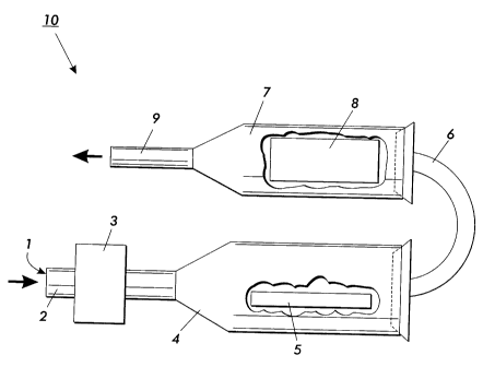
An exemplary embodiment of a treatment system according to the present
invention is depicted in Fig. 1. In this embodiment of the treatment system
10, dry air
is introduced through an opening 1 in a conduit 2. A flow meter 3 is placed in
series
between the opening 1 and a first vessel 4 to control the flow rate of dry air
passing
through the conduit 2 into the vessel 4. The vessel 4 contains a corona
discharge
device 5, and is connected via an adjoining conduit 6 to a second vessel 7.
The '
second vessel 7 contains a photoreceptor 8 and a vent conduit 9. The corona
CA 02362216 2005-O1-13
9
discharge device 5 and the photoreceptor 8 are kept in separate vessels to
insure that the
photoreceptor 8 is only exposed to the effluent of the corona device 5.
Although the vessels in the embodiment of Fig. 1 can be made of various
materials and, can be configured in various shapes, one suitable type of a
vessel is a
glass, tubular shaped vessel. In addition, while various corona devices can be
used
according to the present invention, one suitable corona device is an Enercon
Model Al
corona surface treatment device available from Enercon Industries Corporation.
In operation, a method of treating a charge transport layer of an organic
photoreceptor according to the present invention using the system of Fig. 1
involves
several steps. First, a photoreceptor 8 to be treated is placed in the second
vessel 7.
Next, the corona device 5 is activated to produce a corona effluent. Dry air
is then
introduced through the conduit 2 into the first vessel 4. Although the dry air
can be
introduced into vessel 4 at various flow rates, dry air is preferably
introduced at a flow
rate that is greater than 155 cm3/min, although any suitable flow rate can be
used, as
desired. The dry air transfers the corona effluent from the first vessel
through the
connecting conduit 6 to the second vessel 7. The corona effluent is then
brought into
contact with the outermost layer of the photoreceptor 8 causing surface energy
of the
outermost layer to be increased and causing the surface to be cleaned.
Following the
exposure of the photoreceptor to the corona effluent, the dry air and excess
effluent is
then vented from the second vessel 7 through the vent conduit 9.
The structure of an exemplary imaging member according to the claimed
invention will now be described.
Typically, a flexible or rigid substrate is provided having an electrically
conductive surface. A charge generating layer is then usually applied to the
electrically conductive surface. An optional charge blocking layer can be
applied to
the electrically conductive substrate prior to the application of the charge
generating
layer. If desired, an adhesive layer can be used between the charge blocking
layer and
the charge generating layer. Usually, the charge generating layer is applied
onto the
blocking layer and a charge transport layer is formed on the charge generation
layer
'v 30 (i.e. forming the outermost layer of the photoreceptbr). However, in
some
embodiments, the charge transport layer can be applied prior to or concurrent
with the
charge generating layer, in which case the charge generating layer would
constitute the
outermost layer.
CA 02362216 2001-11-14
The substrate support layer can be opaque or substantially transparent and can
comprise numerous suitable materials having the required mechanical properties
as
well as flexibility. Accordingly, the substrate support layer can comprise a
layer of an
electrically non-conductive or conductive material such as an inorganic or an
organic
5 composition. As electrically non-conducting materials, there can be employed
various
resins known for this purpose including, but not limited to, polyesters,
polycarbonates,
polyamides, polyurethanes, mixtures thereof, and the like. As electrically
conductive
materials there can be employed various resins that incorporate conductive
particles,
including but not limited to, resins containing an effective amount of carbon
black, or
10 metals such as copper, aluminum, nickel, alloys thereof, and the like. The
substrate
support layer can be either of a single layer design, or alternatively, can be
of a multi-
layer design that includes, for example, an electrically insulating layer
having an
electrically conductive layer applied thereon.
The electrically insulating or conductive substrate support layer is
preferably in
the form of a rigid cylinder, drum or belt. In the case of the substrate being
in the
form of a belt, the belt can be seamed or seamless, with a seamless belt being
preferred.
The thickness of the substrate support layer depends on numerous factors,
including desired strength and rigidity, as well as economic considerations.
Thus, this
layer can be of substantial thickness, for example, about 5,000 micrometers or
more,
or it can be of minimum thickness of less than or equal to about 150
micrometers, or
anywhere in between, provided that there are no adverse effects on the final
electrostatographic device. The surface of the substrate support layer is
preferably
cleaned prior to coating to promote greater adhesion of the deposited coating.
Cleaning can be effected by any known process, including, for example, by
exposing
the surface of the substrate layer to plasma discharge, ion bombardment and
the like.
The conductive layer can vary in thickness over substantially wide ranges
depending on the optical transparency and degree of flexibility desired for
the
electrostatographic member. Accordingly, for a photoresponsive imaging device
having an electrically insulating, transparent cylinder, the thickness of the
conductive
layer can be between about 10 angstrom units to about 500 angstrom units, and
more
preferably from about 100 angstrom units to about 200 angstrom units for an
optimum
combination of electrical conductivity and light transmission. The conductive
layer
can be an electrically conductive metal layer formed, for example, on the
substrate by
CA 02362216 2001-11-14
11
any suitable coating technique, such as a vacuum depositing technique. Typical
metals include, but are not limited to, aluminum, zirconium, niobium,
tantalum,
vanadium and hafnium, titanium, nickel, stainless steel, chromium, tungsten,
molybdenum, mixtures thereof, and the like. In general, a continuous metal
film can
S be attained on a suitable substrate support layer, e.g. a polyester web
substrate such as
Mylar available from E. I. du Pont de Nemours & Co., with magnetron
sputtering.
If desired, an alloy of suitable metals can be deposited. Typical metal alloys
can contain two or more metals such as zirconium, niobium, tantalum, vanadium
and
hafnium, titanium, nickel, stainless steel, chromium, tungsten, molybdenum,
and the
like, and mixtures thereof. Regardless of the technique employed to form the
metal
layer, a thin layer of metal oxide generally forms on the outer surface of
most metals
upon exposure to air. Thus, when other layers overlying the metal layer are
characterized as "contiguous" (or adjacent or adjoining) layers, it is
intended that these
overlying contiguous layers can, in fact, contact a thin metal oxide layer
that has
formed on the outer surface of the oxidizable metal layer. Generally, for rear
erase
exposure, a conductive layer light transparency of at least about 15 percent
is
desirable. The conductive layer need not be limited to metals. Other examples
of
conductive layers can be combinations of materials such as conductive indium
tin
oxide as a transparent layer for light having a wavelength between about 4000
Angstroms and about 7000 Angstroms or a conductive carbon black dispersed in a
plastic binder as an opaque conductive layer. A typical surface electrical
conductivity
for conductive layers for electrophotographic imaging members in slow speed
copiers
is about 102 to 103 ohms/square.
After formation of an electrically conductive surface, a hole blocking layer
can
optionally be applied thereto for photoreceptors. Generally, electron blocking
layers
for positively charged photoreceptors allow holes from the imaging surface of
the
photoreceptor to migrate toward the conductive layer. For negatively charged
photoreceptors, the blocking layer allows electrons to migrate toward the
conducting
layer. Any suitable blocking layer capable of forming an electronic barrier to
holes
between the adjacent photoconductive layer and the underlying conductive layer
can
be used. The blocking layer can include, but is not limited to, nitrogen
containing
siloxanes or nitrogen containing titanium compounds such as trimethoxysilyl
propylene diamine, hydrolyzed trimethoxysilyl propyl ethylene diamine, N-
beta(aminoethyl) gamma-amino-propyl trimethoxy silane, isopropyl 4-
aminobenzene
CA 02362216 2005-O1-13
12
sulfonyl, di(dodecylbenzene sulfonyl)titanate, isopropyl di(4-
aminobenzoyl)isostearoyl titanate, isopropyl tri(N-
ethylaminoethylamino)titanate,
isopropyl trianthranil titanate, isopropyl tri(N,N-dimethyl-
ethylamino)titanate,
titanium-4-amino benzene sulfonate oxyacetate, titanium 4-aininobenzoate
isostearate
oxyacetate, [H2N(Cl-i2)4]CI~3S1(OCH3)2 (gamma-aminobutyl)methyl
diethoxysilane,
[H2N(CH2)3]CH3S1(OCH3)? (gamma-aminopropyl)methyl diethoxysilane, mixtures
thereof, and the like, as disclosed in U.S. Patents Nos. 4,291,110, 4,338,387,
4,286,033 and 4,291,110. A preferred blocking layer comprises a reaction
product
between a hydrolyzed silane and the oxidized surface of a metal ground plane
layer.
The oxidized surface inherently forms on the outer surface of most metal
ground plane
layers when exposed to air after deposition.
In a typical flexible photoreceptor belt, the blocking layer can be applied by
any suitable conventional technique such as spraying, dip coating, draw bar
coating,
gravure coating, silk screening, air knife coating, reverse roll coating,
vacuum
15. deposition, chemical treatment and the like. For convenience in obtaining
thin layers,
the blocking layers are preferably applied in the form of a dilute solution,
with the:
solvent being removed after deposition of the coating by conventional
techniques such
as by vacuum, heating and the like. The blocking layers should be continuous
and
have a thickness of less than about 0.2 micrometer because greater thicknesses
can
lead to undesirably high residual voltage.
For rigid photoreceptor drum designs, the blocking layer is typically a
continuous coating layer having a thickness of, for example, less than about 2
micrometers. The blocking layer can be formed of, for example, zirconium
silane or
Luckamide~. A blocking layer having a greater thickness generally requires the
addition of conducting molecules, for example Ti02 doped phenolics, to avoid
undesirably high residual voltage.
An optional adhesive layer can be applied to the hole blocking layer. Any
suitable adhesive layer well known in the art can be used. Typical adhesive
layer
materials include, for example, but are not limited to, polyesters, dupont
49,000
(available from E. I. dupont de Nemours and Company), Vitel~ PE100 available
from
Goodyear Tire & Rubber), polyurethanes, and the like. Satisfactory results can
be
achieved with adhesive layer thickness between about 0.05 micrometer (500
angstrom)
and about 0.3 micrometer (3,000 angstroms). Conventional techniques for
CA 02362216 2005-O1-13
13
applying an adhesive layer coating mixture to the charge blocking layer
include
spraying, dip coating, roll coating, wire wound rod coating, gravure coating,
Bird
applicator coating, and the like. Drying of the deposited coating can be
effected by
any suitable conventional technique such as oven drying, infra red radiation
drying, air
drying and the like.
Any suitable photogenerating layer can be applied to the adhesive or blocking
layer, which in turn can then be overcoated with a contiguous hole (charge)
transport
layer as described hereinafter.
Examples of typical photogenerating layers include, but are not limited to,
inorganic photoconductive particles such as amorphous selenium, trigonal
selenium,
and selenium alloys selected from the group consisting of selenium-tellurium,
selenium-tellurium-arsenic, selenium arsenide and mixtures thereof, and
organic
photoconductive particles including various phthalocyanine pigment such as the
~-
form of metal free phthalocyanine described in U.S. Patent No. 3,357,989,
metal
phthalocyanines such as vanadyl phthalocyanine and copper phthalocyanine,
dibromoanthanthrone, squarylium, quinacridones;available from Dupont under the
tradename Monastral Red, Monastral violet and Monastral Red Y, Vat orange 1
and
Vat orange 3 trade names for dibromo anthanthrone pigments, benzimidazole
perylene, perylene pigments as disclosed in U.S. Patent No. 5,891,594,
substituted 2,4-
diamino-triazines disclosed in U.S. Patent No. 3,442,781, polynuclear aromatic
quinones available from Allied Chemical Corporation under the tradename
Indofast
Double Scarlet, Indofast Violet Lake B, Indofast Brilliant Scarlet and
Indofast
Orange, and the like dispersed in a film forming polymeric binder. Mufti-
photogenerating layer compositions can be used where a photoconductive layer
enhances or reduces the properties of the photogenerating layer. Examples of
this type
of configuration are described in U.S. Patent No. 4,415,639. Other suitable
photogenerating materials known in the art can also be utilized, if desired.
Charge generating binder layers comprising particles or layers comprising a
photoconductive material such as vanadyl phthalocyanine, metal free
phthalocyanine,
benzimidazole perylene, amorphous selenium, trigonal selenium, selenium alloys
such as selenium-tellurium, selenium-tellurium-axsenic, selenium arsenide, and
the
like and mixtures thereof are especially preferred because of their
sensitivity to white
light.
CA 02362216 2005-O1-13
14
Vanadyl phthalocyanine, metal free phthaIocyanine and selenium tellurium
alloys are
also preferred because these materials provide the additional benefit of being
sensitive
to infra-red light.
Any suitable polymeric film forming binder material can be employed as the
matrix in the photogenerating binder layer. Typical polymeric film forming
materials
include, but are not limited to, those described, for example, in U.S. Patent
No.
3,121,006. Thus, typical organic polymeric film forming binders include, but
are not
limited to, thermoplastic and thermosetting resins such as polycarbonates,
polyesters,
polyamides, polyurethanes, polystyrenes, polyarylethers, polyarylsulfones,
polybutadienes, polysulfones, polyethersulfones, polyethylenes,
polypropylenes,
polyimides, polymethylpentenes, polyphenylene sulfides, polyvinyl acetate,
polysiloxanes, polyacrylates, polyvinyl acetais, polyamides, polyimides, amino
resins,
phenylene oxide resins, terephthalic acid resins, phenoxy resins, epoxy
resins,
phenolic resins, polystyrene and acrylonitrile copolymers, polyvinylchloride,
vinylchloride and vinyl acetate copolymers, acrylate copolymers, alkyd resins,
cellulosic film formers, poly(amideimide), styrene-butadiene copolymers,
vinylidenechloride-vinylchloride copolymers, vinylacetate-vinylidenechloride
copolymers, styrene-alkyd resins, polyvinylcarbazole, mixtures thereof, and
the like.
These polymers can be block, random or alternating copolymers.
The photogenerating composition or pigment can be present in the resinous
binder composition in various amounts. Generally, however, the photogenerating
composition or pigment can be present in the resinous binder in an amount of
from
about 5 percent by volume to about 90 percent by volume of the photogenerating
pigment dispersed in about 10 percent by volume to about 95 percent by volume
of
the resinous binder, and preferably from about 20 percent by volume to about
34
percent by volume of the photogenerating pigment is dispersed in about 70
percent by
volume to about 80 percent by volume of the resinous binder composition. In
one
embodiment, about 8 percent by volume of the photogenerating pigment is
dispersed
in about 92 percent by volume of the resinous binder composition.
The photogenerating layer containing photoconductive compositions andlor
pigments and the resinous binder material generally ranges in thickness of
from about
O.I micrometer to about 5.0 micrometers, and preferably has a thickness of
from about
0.3 micrometer to about 3 micrometers. The phatogenerating layer thickness is
CA 02362216 2005-O1-13
generally related to binder content. Thus, for example, higher binder content
compositions generally require thicker layers far photogeneration. Of course,
thickness outside these ranges can be selected providing the objectives of the
present
invention are achieved.
5 Any suitable and conventional technique can be used to mix and thereafter
apply the photogenerating layer coating mixture. Typical application
techniques
include spraying, dip coating, roll coating, wire wound rod coating; and the
like:-
Drying of the deposited coating can be effected by any suitable conventional
technique such as oven drying, infra red radiation drying, air drying and the
like.
10 The electrophotographic imaging member formed by the process of the present
invention generally contains a charge transport layer in addition to the
charge
generating layer. The charge transport layer comprises any suitable organic
polymer
or non-polymeric material capable of transporting charge to selectively
discharge the
surface charge. Charge transporting layers can be formed by any conventional
15 materials aid methods, such as the materials and methods disclosed in U.S.
Patent No.
5,521,047 to Yuh et al. In addition, the charge transporting layers can be
formed as' an
aromatic diamine dissolved or molecularly dispersed in an electrically
inactive
polystyrene film forming hinder, such as disclosed in U.S. Patent No.
5,709,974:
Any suitable and conventional technique can be used to mix and thereafter
apply the charge transport layer coating mixture to the charge generating
layer.
Typical application techniques include spraying, dip coating, roll coating,
wire wound
rod coating, and the like. Preferably, the coating mixture of the transport
layer
comprises between about 9 percent and about 12 percent by weight binder,
between
. about 27 percent and about 3 percent by weight charge transport material,
and
between about 64 percent and about 85 percent by weight solvent for dip
coating
applications. Drying of the deposited coating can be effected by any suitable
conventional technique such as oven drying, infra-red radiation drying, air
drying and
the Like.
Generally, the thickness of the charge transport layer is between about 10 and
about 50 micrometers, but thickness outside this range can also be used. The
charge
. transport layer should preferably be an insulator to the extent that the
electrostatic
charge placed on the charge transport layer is not conducted in the absence of
CA 02362216 2001-11-14
16
illumination at a rate sufficient to prevent formation and retention of an
electrostatic
latent image thereon. In general, the ratio of thickness of the charge
transport layer to
the charge generator layer is preferably maintained from about 2:1 to 200:1
and in
some instances as great as 400:1. In other words, the charge transport layer
is
substantially non-absorbing to visible light or radiation in the region of
intended use
but is "active" in that it allows the injection of photogenerated holes from
the
photoconductive layer, i.e., charge generation layer, and allows these holes
to be
transported through the active charge transport layer to selectively discharge
a surface
charge on the surface of the active layer.
An overcoat layer is applied over the charge transport layer (or over the
otherwise underlying outermost layer, for example where the charge transport
layer
and the charge generating layer are reversed or combined). However, according
to the
present invention, the underlying outermost layer is first surface treated, as
described
above, prior to application of the overcoating layer. The overcoat layer can
comprise,
for example, a dihydroxy arylamine dissolved or molecularly dispersed in a
polyamide
matrix. The overcoat layer can be formed from a coating composition comprising
an
alcohol soluble film forming polyamide and a dihydroxy arylamine.
In these embodiments, any suitable alcohol soluble polyamide film forming
binder capable of forming hydrogen bonds with the hydroxy functional materials
can
be utilized in the overcoating. The expression "hydrogen bonding" is defined
as the
attractive force or bridge occurring between the polar hydroxy containing aryl-
amine
and a hydrogen bonding resin in which the hydrogen atom of the polar hydroxy
arylamine is attracted to two unshared electrons of a resin containing
polarizable
groups. The hydrogen atom is the positive end of one polar molecule and forms
a
linkage with the electronegative end of the polar molecule. The polyamide used
in the
overcoatings should also have sufficient molecular weight to form a film upon
removal of the solvent and also be soluble in alcohol. Generally, the weight
average
molecular weights of polyamides vary from about 5,000 to about 1,000,000.
Since
some polyamides absorb water from the ambient atmosphere, its electrical
property
can vary to some extent with changes in humidity in the absence of a
polyhydroxy
arylamine charge transporting monomer, the addition of charge transporting
polyhydroxy arylamine minimizes these variations. The alcohol soluble
polyamide
should be capable of dissolving in an alcohol solvent, which also dissolves
the hole
transporting small molecule having multi hydroxy functional groups. The
polyamide
CA 02362216 2005-O1-13
17
polymers required for the overcoatings are characterized by the presence of
amide
groups, -CONH. Typical polyamides include the various Elvamide resins, which
are
nylon multipolymer resins, such as alcohol soluble ElvamideTM and Elvamide~ TH
Resins. ElvamideTM resins are available from E. I. Dupont Nemours and Company.
Other examples of polyamides include Elvamide~M 8061, ElvamideTM 8064, and
Elvamide~ 8023. One class of alcohol soluble polyamide polymer is disclosed in
U.S. Patent No. 5,709,974.
The polyamide should also be soluble in the alcohol solvents employed.
Typical alcohols in which the polyamide is soluble include, for example,
butanol,
ethanol, methanol, and the like. Typical alcohol soluble polyamide polymers
having
methoxy methyl groups attached to the nitrogen atoms of amide groups in the
polymer backbone prior to cros~linking include, for example, hole insulating
alcohol
soluble polyamide film forming polymers include, for example, LuckamideTM 5003
from Dai Nippon Ink, Nylon 8 with methylmethoxy pendant groups, CM4000TM from
Toray Industries, Ltd. and CM8000TM from Toray Industries, Ltd., and other N-
methoxymethylated polyamides, such as those prepared according to the method
described in Sorenson and Campbell "Preparative Methods of Polymer Chemistry"
second edition, pg 76, John Wiley & Sons Inc. 1968, and the like, and mixtures
thereof. Other polyamides axe Elvamides from E. I. Dupont de Nemours & Co.
These
polyarnides can be alcohol soluble, for example, with polar functional groups,
such as
methoxy, ethoxy and hydroxy groups, pendant from the polymer backbone. These
film forming polyamides are also soluble in a solvent to facilitate
application by
conventional coating techniques. Typical solvents include, for example,
butanol,
methanol, butyl acetate, ethanol, cyclohexanone, tetrahydrofuran, methyl ethyl
ketone, and the like and mixtures thereof.
When the overcoat layer contains only polyamide binder material, the layer
tends to absorb moisture from the ambient atmosphere and becomes soft and
hazy.
This adversely affects the electrical properties, and the sensitivity of the
overcoated
photoreceptor. To overcome this, the overeoating of this invention also
includes a
dihydroxy arylamine, as disclosed in U.S. Patents Nos. 5,709,974, 4,871,634
and
4,588,666.
The concentration of the hydroxy arylamine in the overcoat can be between
about 2 percent and about 50 percent by weight based on the total weight of
the dried
overcoat. Preferably, the concentration of the hydroxy arylamine in the
overcoat layer
CA 02362216 2001-11-14
18
is between about 10 percent by weight and about 50 percent by weight based on
the
total weight of the dried overcoat. When less than about 10 percent by weight
of
hydroxy arylamine is present in the overcoat, a residual voltage can develop
with
cycling resulting in background problems. If the amount of hydroxy arylamine
in the
overcoat exceeds about 50 percent by weight based on the total weight of the
overcoating layer, crystallization can occur resulting in residual cycle-up.
In addition,
mechanical properties, abrasive wear properties are negatively impacted.
The thickness of the continuous overcoat layer selected can depend upon the
abrasiveness of the charging (e.g., bias charging roll), cleaning (e.g., blade
or web),
development (e.g., brush), transfer (e.g., bias transfer roll), etc., system
employed and
can range up to about 10 micrometers. A thickness of between about 1
micrometer
and about 5 micrometers in thickness is preferred. Any suitable and
conventional
technique can be used to mix and thereafter apply the overcoat layer coating
mixture
to the charge generating layer. Typical application techniques include
spraying, dip
coating, roll coating, wire wound rod coating, and the like. Drying of the
deposited
coating can be effected by any suitable conventional technique such as oven
drying,
infrared radiation drying, air drying and the like. The dried overcoating of
this
invention should transport holes during imaging and should not have too high a
free
carrier concentration. Free Garner concentration in the overcoat increases the
dark
decay. Preferably the dark decay of the overcoated layer should be the same as
that of
the unovercoated device.
The photoreceptors of the present invention can comprise, for example, a
charge generator layer sandwiched between a conductive surface and a charge
transport layer, as described above, or a charge transport layer sandwiched
between a
conductive surface and a charge generator layer. This structure can be imaged
in the
conventional xerographic manner, which usually includes charging, optical
exposure
and development.
Other layers can also be used, such as a conventional electrically conductive
ground strip along one edge of the belt or drum in contact with the conductive
layer,
blocking layer, adhesive layer or charge generating layer to facilitate
connection of the
electrically conductive layer of the photoreceptor to ground or to an
electrical bias.
Ground strips are well known and usually comprise conductive particles
dispersed in a
film forming binder.
CA 02362216 2001-11-14
19
In some cases, such as flexible photoreceptor belts, an anti-curl back coating
can be applied to the side opposite the photoreceptor substrate support layer
to provide
flatness and/or abrasion resistance. These overcoating and anti-curl back
coating
layers are well known in the art and can comprise thermoplastic organic
polymers or
inorganic polymers that are electrically insulating or slightly
semiconductive.
Overcoatings are continuous and generally have a thickness of less than about
10
micrometers.
Any suitable conventional electrophotographic charging, exposure,
development, transfer, fixing and cleaning techniques can be used to form and
develop electrostatic latent images on the imaging member of this invention.
Thus,
for example, conventional light lens or laser exposure systems can be used to
form the
electrostatic latent image. The resulting electrostatic latent image can be
developed by
suitable conventional development techniques such as magnetic brush, cascade,
powder cloud, and the like.
The present invention enhances the interfacial adhesion between overcoat
materials and the outermost (underlying) layer as well as the interfacial bond
strength
between the anticurl backing layer and the substrate support layer of an
organic
photoreceptor using the effluents of a corona discharge. More specifically,
the present
invention is directed to the use of effluents of a corona discharge to treat a
surface of
the outermost layer of an organic photoreceptor prior to the application and
heat
treatment of wear-resistant overcoat materials to achieve necessary adhesion
while
maintaining an overcoat's wear-resistant properties.
While the invention has been described in conjunction with the specific
embodiments described above, it is evident that many alternatives,
modifications and
variations are apparent to those skilled in the art. Accordingly, the
preferred
embodiments of the invention as set forth above are intended to be
illustrative and not
limiting. Various changes can be made without departing from the spirit and
scope of
the invention.
The examples set forth hereinbelow and are illustrative of different
compositions and conditions that can be used in practicing the invention. All
proportions are by weight unless otherwise indicated. It will be apparent,
however,
that the invention can be practiced with many types of compositions and can
have
many different uses in accordance with the disclosure above and as pointed out
hereinafter.
CA 02362216 2001-11-14
EXAMPLES
Example 1:
An electrophotographic imaging member sheet is prepared. The imaging
member includes a support substrate 6063 honed aluminum alloy 340 mm in length
5 with a diameter of 30 mm. The first layer, an undercoat layer (UCL) used as
an
electrical and blocking layer, is applied, as like all other coatings are
applied, by dip
coating technology. A "three-component" UCL containing polyvinyl butyral (6
weight percent), zirconium acety acetonate (83 weight percent) and gamma-
aminopropyl triethoxy silane ( 11 weight percent) are mixed, in the order
listed, with
10 n-butyl alcohol in 60:40 (by volume) solvent to solute weight ratio for the
UCL. The
UCL is applied in a thickness of approximately one micrometer to the honed
substrate
by dip coating. The substrate is next coated with about 0.2 micrometer thick
charge
generating layer (CGL) of hydroxygallium phthalocyanine (OHGaPC) and a
terpolymer VMCH available from Union Carbide of: vinyl chloride (83 weight
15 percent), vinyl acetate ( 16 weight percent) and malefic anhydride ( 1
weight percent),
dissolved in n-butyl acetate (4.5 weight percent solids) in a 60:40 weight
ratio (60
OHGaPC : 40 VMCH). The CGL is subsequently coated with a 24 micrometer thick
(after drying) charge transport layer (CTL) of polycarbonate derived from bis
phenyl Z
(PCZ, available from Mitsubishi Chemicals) and N,N'-Biphenyl-N,N'-bis(3-
20 methylphenyl)-(1,1'-biphenyl)-4,4' diamine dissolved in tetrahydrofuran.
After drying the charge transport layer, the charge transport layer is exposed
to
corona discharge treatment effluent. The corona discharge is operated at -5 kV
for an
exposure time of three minutes.
Twenty-four hours after the corona discharge treatment, an overcoating layer
is
applied to the surface treated charge transport layer. The overcoating layer
is coated
using a solution of Luckamide~ (a polyamide film forming polymer available
from
Dai Nippon Ink). The overcoating layer is dried at 110°C for 30
minutes.
The thus prepared electrophotographic imaging member sheet is tested for
adhesion of the overcoating layer to the underlying charge transport layer.
The
adhesion data is given in Table 1, below.
Examples 2-4:
Electrophotographic imaging member sheets are prepared as in Example 1
above, except that the corona discharge treatment time is set at 6, 12 or 24
minutes,
respectively, for Examples 2, 3 and 4.
CA 02362216 2001-11-14
21
The thus prepared electrophotographic imaging member sheets are tested for
adhesion of the overcoating layer to the underlying charge transport layer.
The
adhesion data is given in Table l, below.
Comparative Example 1:
An electrophotographic imaging member sheet is prepared as in Example 1
above, except that the corona discharge treatment is not performed on the
charge
transport layer.
The thus prepared electrophotographic imaging member sheet is tested for
adhesion of the overcoating layer to the underlying charge transport layer.
The
adhesion data is given in Table l, below.
Table 1
Example Corona Adhesion (g/cm)
Treatment
Time
(min)
1 3 76 58 CNP
2 6 CNP CNP CNP
3 12 CNP
4 24 CNP CNP
Com 1 None 4.1 8.5 3.1
* CNP = Cannot
Peal
Examples 5-9:
Electrophotographic imaging member sheets are prepared as in Example 1
above, except that the corona discharge treatment time is varied, and the
overcoating
layer is applied to the surface treated charge transport layer immediately
after the
surface treatment is completed. The corona discharge treatment times for the
Examples are set forth in Table 2 below.
The thus prepared electrophotographic imaging member sheets are tested for
adhesion of the overcoating layer to the underlying charge transport layer.
The
adhesion data is given in Table 2, below.
Comparative Example 2:
An electrophotographic imaging member sheet is prepared as in Examples S-9
above, except that the corona discharge treatment is not performed on the
charge
transport layer.
CA 02362216 2005-O1-13
22
The thus prepared eleetrophotographic imaging member sheet is tested for
adhesion of the overcoating layer to the underlying charge transport layer.
The
adhesion data is given in Table 2, below.
Table 2
Example Corona Adhesion
Treatment (g/cm)
Time (min)
0.25 0 0.3
6 0.5 1.1 0.8 0.5
7 1 10 14 16
8 2 CNP CNP CNP 5
9 4 CNP CNP CNP CNP
Com 2 0 0 0.3
5 * CNP = Cannot Peal
Comparative Examt~le 3
An electrophotographic imaging member web is prepared by providing a 0.02
micrometer thick titanium layer coated on a PET polyester substrate support
layer
Melinex~ 442, available from TCI Americas, Inc.) having a thickness of 3 mils
(76.2
micrometers) and applying thereto, using a %2 mil gap Bird applicator, a
solution
containing 10 grams gamma aminopropyltriethoxy silane, 10.1 grams distilled
water, 3
grams acetic acid, 684.8 grams of 200 proof denatured alcohol and 200 grams
heptane.
This layer is allowed to dry for 5 minutes at 135°C in a forced air
oven. The resulting
blocking layer has an average dry thickness of 0.05 micrometer measured with
an
ellipsometer.
An adhesive interface layer is prepared by applying with a ~h mil gap Bird
applicator to the blocking layer a wet coating containing 5 percent by weight
based on
the total weight of the solution of polyester adhesive (Mor-Ester 49,000,
available
from Morton International, lnc.) in a 70:30 volume ratio mixture of
tetrahydrofuranlcyclohexanone. The adhesive interface layer is allowed to dry
for 5
minutes at 135°C in a forced air oven. The resulting adhesive interface
layer has a dry
thickness of 0.065 micrometer.
The adhesive interface layer is thereafter coated with a photogenerating layer
containing 7.5 percent by volume trigonal selenium, 25 percent by volume N,N'-
diphenyl-N,N'-bis(3-methylphenyl)-1,1'-biphenyl-4,4'-diamine, and 67.5 percent
by
volume polyvinylcarbazole. This photogenerating layer is prepared by
introducing 8
CA 02362216 2005-O1-13
23
grams polyvinyl carbazole and 140 mls of a 1:1 volume ratio of a mixture of
tetrahydrofuran and toluene into a 20 oz. amber bottle. To this solution is
added 8
grams of trigonal selenium and 1,000 grams of 1/8 inch (3.2 millimeter)
diameter
stainless steel shot. This mixture is placed on a ball mill for 72 to 96
hours.
Subsequently, 50 grams of polyvinyl carbazole and 2.0 grams of N,N'-diphenyl-
N,N'-
bis(3-methylphenyl)-1,1'-biphenyl-4,4'-diamine are dissolved in 75 ml of 1:1
volume
ratio of tetrahydrofuranltoluene. This slurry is placed on a shaker for 10
minutes. The
resulting slurry is thereafter applied to the adhesive interface Layer by
using a I/z mil
gap Bird applicator to form a coating layer having a wet thickness of 0.5 mil
( 12.7
micrometers). However, a strip about 10 mm wide along one edge of the
substrate
bearing the blocking layer and the adhesive layer is deliberately left
uncoated by any
of the photogenerating layer material to facilitate adequate electrical
contact by the
ground strip layer that is applied later. This photogenerating layer is dried
at 135°C
for S minutes in a forced air oven to form a dry photogenerating layer having
a
thickness of 2.0 micrometers.
This coated imaging member web is simultaneously overcoated with a charge
transport layer and a ground strip layer using a 3 miTgap Bird applicator. The
charge
transport layer is prepared by introducing into an amber glass bottle a weight
ratio of
1:1 N,N'-diphenyl-N,N'-bis(3-methylphenyl)-1,1'-biphenyl-4-4'-diamine and
Makrolon~ 5705, a polycarbonate resin having a molecular weight of from about
50,000 to 100,000 commercially available from Farbenfabriken Bayer A.G. The
resulting mixture is dissolved to give a 15 percent by weight solid in 85
percent by
weight methylene chloride. This solution is applied onto the photogenerator
layer to
form a coating which upon drying has a thickness of 24 micrometers.
The approximately 10 mm wide strip of the adhesive layer left uncoated by the
photogenerator layer is coated with a ground strip layer. This ground strip
layer, after
drying at 135°C in a forced air oven for 5 minutes, has a dried
thickness of about 14
micrometers. This ground strip is electrically grounded, by conventional means
such as
a carbon brush contact device during a conventional xerographic imaging
process.
~ anticurl backing layer coating solution is prepared by combining 8.82 grams
of polycarbonate resin of 4,4'-isopropylidene diphenol (MakrolonTM 5705,
having a
molecular weight of about 120,000 and available from Bayer AG), 0.092 gram of
copolyester resin (VitelTM PE-100, available from Goodyear Tire and Rubber
Company) and 90.1 grams of methylene chloride in a glass container to form a
coating
solution
CA 02362216 2001-11-14
24
containing 8.9 percent solids. The container is covered tightly and placed on
a roll
mill for about 24 hours until the polycarbonate and polyester are dissolved in
the
methylene chloride to form the anti-curl coating solution. The anticurl
backing layer
coating solution is applied to the rear surface (side opposite the
photogenerator layer
and charge transport layer) of the imaging member web with a 3 mil gap Bird
applicator and dried at 135°C for about 5 minutes in a forced air oven
to produce a
dried film thickness of about 13.5 micrometers and containing approximately 1
weight
percent Vital PE-100 adhesion promoter, based on the total weight of the dried
anticurl backing layer. The resulting electrophotographic imaging member had a
structure similar to that schematically shown in Figure 1 and was used to
serve as an
imaging member control.
EXAMPLE 10:
An electrophotographic imaging member web is prepared according to the
procedures and using the same materials as those described in Comparative
Example
3, with the exception that the backside of the PET polyester substrate support
layer is
exposed to corona effluents emitted from a Corotron charging device, to clean
and
activate the surface of the substrate support layer, prior to the application
of the
anticurl backing layer coating. The power supplied to the charging device is
about 6
kv and the transport speed of the charging device traversing over the
substrate support
layer surface is about S inches per second.
EXAMPLE 11:
The electrophotographic imaging member webs of Comparative Example 3
and Example 10 are evaluated for anticurl backing layer adhesion to the
substrate
support layer by 180° peel strength measurement. The peel strengths
obtained for the
anticurl backing layer of each of these imaging member webs are assessed for
comparison.
The procedures for 180° peel strengths measurement are carried out by
cutting
a minimum of three 0.5 inch ( I .2 cm.) x 6 inches ( 15.24 cm) imaging member
samples from each of Comparative Examples 3 and Example 10. For each sample,
the anticurl backing layer is partially stripped from the test sample with the
aid of a
razor blade and then hand peeled to about 3.5 inches from one end to expose
the
substrate support layer inside the sample. This stripped sample is then
secured to a 1
CA 02362216 2001-11-14
inch (2.54 cm) x 6 inches ( 15.24 cm) and 0.05 inch (0.254 cm) thick aluminum
backing plate (having the charge transport layer facing the backing plate)
with the aid
of two sided adhesive tape. The end of the resulting assembly, opposite the
end from
which the anticurl backing layer is not stripped, is inserted into the upper
jaw of an
5 Instron Tensile Tester. The free end of the partially peeled anticurl
backing layer is
inserted into the lower jaw of the Instron Tensile Tester. The jaws are then
activated
at a one inch/mm crosshead speed, a two inch chart speed and a load range of
200
grams, to peel the sample at least two inches at an angle of 180°. The
load recorded is
then calculated to give the peel strength of the test sample. The peel
strength is
10 determined to be the load required for stripping the anticurl backing layer
off from the
substrate support layer divided by the width ( 1.27 cm) of the test sample.
The results obtained for 180° peel strength between the anticurl
backing
layer (ACBL) and the substrate support layer (PET), and wear resistance are
listed in
Table 3 below:
15 TABLE 3
Example Corona Peel Strength
Treatment ACBL/PET
on PET ( ms/cm)
Com . 3 None g.4
10 Yes 29.3
The data listed in the table above show that the peel strength of the anticurl
20 backing layer of the invention imaging member of Example 10 is
substantially
increased. The peel strength increase from 8.4 gms/cm for the test sample of
Comparative Example 3 to high of 29.3 gms/cm for the test sample of Example 10
represents a 3.5 times anticurl backing layer adhesion improvement through the
simple corona effluent exposure on the back surface of the imaging member
substrate
25 support layer moments before the application of anticurl backing layer
coating
solution. It is important to point out that the solvent (methylene chloride)
used for the
anticurl backing layer costing solution preparation is not a solvent that
could dissolve
the PET.