Note: Descriptions are shown in the official language in which they were submitted.
CA 02362222 2001-11-14
Case 1940
CM/ca
CORRELATION AND DEMODULATION CIRCUIT FOR A
RECEIVER FOR SIGNALS MODULATED BY A SPECIFIC CODE
The invention concerns a correlation and demodulation circuit for a receiver
for
signals modulated by a first code of a determined repetition length, said
first code
defining a source transmitting said signals. This circuit includes a
correlation stage
connected to control means in particular for configuring said correlation
stage in
normal operating mode or test mode. In normal operating mode, said stage is
intended
to receive intermediate signals corresponding to the modulated signals shaped
in the
receiver modulated signal receiving means. The intermediate signals are then
correlated in a correlator control loop of said correlation stage with a first
code replica
generated by a code generator.
The signals which are modulated in particular tv the carrier frequency, and
which are transmitted by one or several transmitter sources, usually include
messages
which have to be demodulated in the correlation and demodulation circuit. The
code
which modulates said signals to define the transmitter source is usually a
pseudo-
random code. This determined repetition length code is unique for each
transmitter
source so as to be able to recognise which transmitter source the signals
received by
the receiver are coming from. They may be for example signals in the
telecommunication field or positioning signals using satellites, such as GPS
type
signals.
In the case of GPS receivers, the radio-frequency signals are transmitted by
several satellites placed in orbit which are distinguished frorri'each other
by a specific
pseudo-random code, called the Gold code, modulated on the carrier frequency
signals. The Gold code is a digital signal which is formed of 1023 chips and
which is
repetitioned every millisecond. The chips have values of 1 or 0 like a bit.
All the Gold
codes have the characteristic of being orthogonal which consequently means
that by
correlating them with each other the correlation result gives a value close to
0. This
characteristic allows several radio-frequency signals simultaneously coming
from
several satellites to be processed independently for example in several
correlation
channels of the same receiver.
The GPS signals supply position and time data to a receiver for calculating
operations of the X, Y and Z position, speed and universal time. However, in
order to
determine position and time, the receiver has to obtain data from at least
four visible
satellites.
In various fields of use of specific code modulated signal receivers, such as
radio-frequency signals, one has to assure that the parts of the receiver
which allow in
CA 02362222 2001-11-14
-2-
particular the messages to be extracted from the received signals, work
properly.
Operating tests may be performed on said receiver parts either before or after
the
assembly thereof. Of course, said receiver parts have had to undergo several
preliminary steps of elementary tests before their operation can be checked
generally.
During use of a GPS receiver, an operating test of said receiver has to be
performed in close to real conditions in order to assure that each channel of
a
correlation stage is working properly. If this operating test is successful,
this allows the
validity of the position, speed and time calculations for example to be
guaranteed to
the user of the receiver.
By way of example, in particular in the field of telecommunications, US Patent
No. 4,100,531 discloses means for measuring the bit error rate of digital
equipment,
such as a data transmission device. This equipment is tested using pseudo-
random
code (PRN code) test signals supplied by a transmitter and received by a
receiver to
be tested. The receiver tested generates a PRN code replica to be correlated
in a
correlation stage with the signals modulated by the PRN code of determined
length.
One drawback of this equipment is that the encoded test signals are sent by an
external transmitter to the receiver in order to be tested, which does not
allow the test
time to be significantly reduced. Moreover, another drawback is that the
transmitted
signals have to be the image of the real communication signals to constitute a
test
representative of the receiver's operation. This inevitably involves having
additional
noise on the test signals, which is often difficult to produce.
In the field of GPS type receivers, US Patent No. 5,093,800 discloses a test
apparatus capable of generating GPS type radio-frequency signals. These GPS
signals generated by the apparatus are intended to be received by a GPS
receiver to
be tested. In order to do this, the apparatus also includes data relating to
the satellites
so as to be able to generate and transmit signals corresponding to the encoded
signals transmitted by several satellites to the receiver.
One drawback noted with this test apparatus lies in the fact that in order to
be
able to check that the correlation stage of the receiver is working properly,
the test
signals are radio-frequency signals equivalent to the radio-frequency signals
transmitted by satellites. This obviously involves generating additional noise
with the
radio-frequency signals generated in the apparatus in order to check that the
correlation stage is working properly. Moreover, another drawback is that the
receiver
operating test time is relatively long since it is dependent on the repetition
length of the
pseudo-random code, i.e. the Gold code. If the receiver is mounted in a device
powered by a battery or an accumulator, the long test time may also run down
said
battery or said accumulator unnecessarily.
CA 02362222 2001-11-14
-3-
One object of the invention consists in providing a correlation and
demodulation circuit for a receiver for signals modulated by a code capable of
reducing as far as possible the test time representing the operation of said
circuit
overcoming the drawbacks of the test devices or methods of the prior art.
Moreover,
by effecting an operating test of said circuit, parameters linked to the
received signal
noise may be taken into account.
This object, in addition to others are achieved by the correlation and
demodulation circuit described hereinbefore which is characterised in that in
test
phase, said code generator is adapted via control means to generate a replica
of a
second repetition code shorter than the first code for correlation operations
with test
intermediate signals modulated by the second repetition code shorter than the
first
code and supplied to the correlation stage so as to perform a test
representative of the
closed loop operation of the correlation stage more quickly than with signals
modulated by the first code.
One advantage of the correlation and demodulation circuit is that the closed
loop test time of the correlation stage is greatly reduced. This allows the
operating
state of said circuit, and thus of the receiver containing it, to be known
quickly.
In the case of a GPS type radio-frequency signal receiver, the correlation and
demodulation circuit test time may be relatively long if the pseudo-random
code
repetition length is equivalent to the Gold code. Moreover, this test time is
also long if
said circuit includes several correlation channels in the correlation stage.
This is why
the intermediate test signals are supplied to the correlation stage of the
circuit with a
pseudo-random code of reduced length for a quick check off, the circuit's
operation.
Since the radio-frequency signals also include noise, the reduced pseudo-
random code length may be defined so as to take account of this noise. The
reduced
code test signals, which are generated without any.noise, allow correlation
stage
integrator counter output signals to be provided whose power is close to the
power of
the real output signals which include noise. Preferably, the pseudo-random
code
repetition length of the test signals is 31 chips, while that of the Gold code
is 1023
chips.
These intermediate test signals may be generated outside the correlation and
demodulation circuit or preferably inside the circuit by integrated test
signal generating
means. These test signal generating means only take a small amount of space in
the
correlation and demodulation circuit, since they are formed of only forty or
so logic
gates or flip-flops, while the circuit has close to 2 million transistors.
These test signal
generating means are switched on by the control means, i.e. by the
microprocessor
means.
CA 02362222 2001-11-14
-4-
Advantageously, said test signal generating means may be switched on at
periods of time programmed in the microprocessor means. When said circuit is
mounted in the complete receiver, switching-on of said test signal generating
means
prevents intermediate signals being sent by the receiving means of the
receiver to said
circuit. Thus, in test phase, the circuit only receives the intermediate test
signals
originating from the test signal generating means.
These test signals are imposed identically in all the channels of the
correlation
stage for a simultaneous test of the channels. The microprocessor controls
each
channel's code generator, so that it generates a replica of the reduced pseudo-
random
code for each channel in test phase.
It is to be noted that no test signals are provided from outside the complete
receiver. Conversely, noise-free operating check test signals are preferably
applied
instead of the conventional intermediate signals to the correlation and
demodulation
circuit.
The reduction in the correlation and demodulation circuit test time is in
theory
necessary when the circuit is mounted in a modulated signal receiver in order
to
perform a test phase quickly. This reduction in the test time may prevent too
much
energy being consumed in an accumulator or storage-battery if the receiver is
mounted in a portable object, such as a watch or a telephone. However, the
correlation and demodulation circuit can also be tested prior to being mounted
in the
receiver with noise-free test signals supplied to the correlation stage
corresponding to
conventional intermediate signals.
A user can also, on his own initiative, perform a complete test of the
receiver
correlation and demodulation circuit at any time.
The objects, advantages and features of the correlation and demodulation
circuit will appear more clearly in the following description of embodiments
of said
circuit illustrated by the drawings, in which:
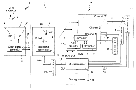
- Figure 1 shows schematically a radio-frequency signal receiver with a
correlation and demodulation circuit according to the invention;
- Figure 2 shows schematically the electronic elements of the test signal
generator of the circuit according to the invention;
- Figure 3a shows a reduced PRN code generator of the test signal generating
means according to the invention;
- Figure 3b shows a PRN code generator which can be configured in normal
operating mode and in test mode for each channel of the correlation stage of
the
circuit according to the invention; and
CA 02362222 2001-11-14
-5-
- Figure 4 shows schematically the elements of a correlator of the correlation
stage according to the invention.
In the following description, the embodiments of the correlation and
demodulation circuit will be explained with reference to a GPS type radio-
frequency
signal receiver. It is to be noted that several elements of the receiver which
are known
to those skilled in the art in this technical field will not be explained in
detail in said
description.
In this type of GPS receiver, the received radio-frequency signals, which are
modulated by a pseudo-random code, called the Gold code, further include
messages
to be demodulated by the correlation and demodulation circuit. The messages
from at
least four satellites thus allow microprocessor means of the circuit to
calculate in
particular the X, Y and Z position, the speed of the receiver andlor the time.
However,
the use of such a correlation and demodulation circuit may also be envisaged
in other
types of receivers for signals modulated by a code of determined repetition
length. For
example, the correlation and demodulation circuit may be used in a
telecommunication
receiver, or in a measuring receiver which use light signals carrying a
determined
code, or in other fields.
The GPS type receiver with the correlation and demodulation circuit is shown
schematically in Figure 1. It is formed of an antenna 2 for receiving GPS
radio-
frequency signals originating from several satellites, means 3 for receiving
and
shaping the radio-frequency signals supplied by antenna 2, and a correlation
and
demodulation circuit 6 receiving intermediate signals IF in complex form at a
frequency
of the order of 400 kHz from receiving means 3.
In receiving means 3, a first electronic circuit 4' first converts the radio-
frequency signals from a frequency 1,57542 GHz into a frequency for example of
179
MHz. A second electronic circuit IF 4" carries out a double conversion to
adjust the
GPS signals first to a frequency of 4.76 MHz then finally to a frequency of
400 kHz by
sampling at 4.36 MHz. Intermediate complex signals IF sampled and quantified
at a
frequency of the order of 400 kHz are thus supplied to the correlation and
demodulation circuit. The intermediate complex signals IF are thus formed of
an in-
phase signal I and a quarter-phase signal Q represented in the Figure by a
bold line
intersected by an oblique line defining 2 bits. However, these intermediate
signals IF
could be defined over 4 bits if a 2-bit conversion had been performed in a
preceding
stage, or 2n bits (n being an integer greater than 1 ).
For the frequency conversion operations, a clock signal generator 5 forms part
of radio-frequency receiving and shaping means 3. This generator is provided
for
example with a quartz oscillator which is not shown, calibrated to a frequency
of the
CA 02362222 2001-11-14
-6-
order of 17.6 MHz. Two clock signals CLK and CLK16 are supplied to the
correlation
and demodulation circuit to clock all of the circuit's operations. The first
clock
frequency CLK may have a value of 4.36 MHz, while the second clock frequency
may
be fixed at 16 times less, i.e. 272.5 kHz used for a large part of the
correlation stage in
order to save on energy consumption.
It is to be noted that the signals supplied by first circuit 4' give, for
example in
half of the cases, signals of different parity (+1 and -1) with 2 output bits
(+3; +1; -1; -3)
with 4 output bits. Account must therefore be taken of this parity for the GPS
signal
demodulating operations in the receiver.
Said correlation and demodulation circuit 6 includes a correlation stage 7
formed of 12 channels 7', a data transfer bus 10 connecting each channel to a
respective buffer register 11, and a data bus 13 connecting each buffer
register to
microprocessor means 12. Storage means 18 connected to the microprocessor form
part of microprocessor means 12 in order to store for example data relating to
each
satellite placed in orbit and carrier frequency and pseudo-random code
parameters for
each satellite. All of the elements forming the correlation and demodulation
circuit can
be made on a single semiconductor substrate, such as a silicon substrate.
At the input of correlation and demodulation circuit 6 are placed test signal
generating means 14 which include a test signal generator 15 and a multiplexer
16.
Multiplexer 16 of test signal generating means 14 receives, at an input,
intermediate
signals IF supplied by receiving means 3 and at another input intermediate
test signals
IF,es,. Said multiplexer 16 is controlled by a control signal Test supplied by
control
means integrated in microprocessor means 12 through control buses 19 and a
buffer
register 11'. Multiplexer 16 could also be integrated in test signal generator
15 if
required.
In normal operating mode without control signal Test, intermediate signals IF
representative of the radio-frequency signals transmitted by several
satellites are
transmitted by multiplexer 16 to correlation stage 7 for all the channels 7'.
Certain
channels are configured differently in normal operating mode via
microprocessor 12 so
that they each search a visible satellite using intermediate signals IF in
order to
demodulate the received GPS messages. Conversely, when microprocessor 12
orders
a test phase, microprocessor 12 sends test control signals in particular to
test signal
generating means 14 via control buses 19. In this test phase, test signal
generator 15
is thus switched on, and multiplexer 16 receiving test signal Test transmits
only
intermediate test signals IFtest generated by generator 15 to correlation
stage 7. Said
test signal generator will be explained in more detail with reference to
Figure 2.
CA 02362222 2001-11-14
- 7 -
Once switched on, test signal generator 15 generates intermediate test signals
IFtest instead of the conventional intermediate signals to perform a test
representative
of the correlation stage in a closed loop. These test signals IFtest are
modulated with a
pseudo-random code of shorter repetition length than the Gold code in order to
perform a closed loop test more quickly. Preferably, the reduced pseudo-random
code
repetition length is 31 chips, i.e. 25-1, whereas the Gold code has a
repetition length of
1023 chips, i.e. 2'°-1.
In the 1023 chips, close to 1000 chips, in proportion, may be considered as
equivalent to the radio-frequency signal noise. Consequently, a reduced code
of 31
chips has been chosen in order to be able to provide noise-free intermediate
test
signals for a test which is representative of the correlation stage.
Of course, for other fields of use of the correlation and demodulation
circuit, the
repetition length of the reduced second pseudo-random code may be 2~"-"'~-1,
whereas
the repetition length of the first pseudo-random code of the received signals
is 2"-1.
The numbers n and m are integer numbers with n greater than 3 and m taking a
determined value between 1 and n-1.
In test phase, microprocessor 12 sends test control signals TMS to test
selectors 17 each placed in a respective channel 7'. Each channel 7' includes
a
correlator 8 receiving signals IF or IF,est and preferably a controller 9
intended to set
into operation via a dedicated material, in particular a signal processing
algorithm for
acquiring a satellite signal and tracking said satellite detected by the
channel. Test
selectors 17 each connected to a respective correlator 8 have the task of
supplying
instructions CS to said correlator in particular for configuring,a pseudo-
random code
generator, which will be explained in more detail with reference to Figure 3b.
In normal operation, no instructions CS are transmitted by selector 17 to
correlator 8, which means that the code generator is intended to generate a
code
replica having an equivalent repetition length to the Gold code. In test phase
however,
upon the command of microprocessor 12, selector 17 sends instructions CS for '
configuring the code generator so that it generates a pseudo-random code
replica
having a shorter repetition length than the Gold code. This reduced pseudo-
random
code must thus be a pseudo-random code modulated on the intermediate test
signals
in test phase.
Control signals TMS are in theory defined as a two-bit control word for normal
operation or various test modes. If TMS equals 00 in binary digits, then no
test
instruction CS is transmitted for normal operation. If TMS equals 11 in binary
digits,
the closed loop test mode is imposed to check that all the channels 7' of
correlation
stage 7 are working properly with intermediate test signals IF,es, introduced
at the
CA 02362222 2001-11-14
input. If TMS equals 01 in binary digits, a test can be undertaken of
correlator module
8 of each channel via a test vector generator which is not shown, controlled
by
microprocessor 12. If TMS equals 10 in binary digits, a test can be undertaken
of
controller module 9 of each channel via the test vector generator. In the
present
invention, the signals TMS preferably take the values 00 or 11.
In an alternative embodiment which is not shown, all the selectors 17 could
form part of microprocessor means 12. Likewise, instructions CS for each
correlator 8
could transit via buses 10 and 13.
At the same time that selector 17 sends instructions CS, microprocessor 12
transmits via buses 13 and 10 parameters relating to the pseudo-random code to
be
searched, and to the carrier frequency of the intermediate test signals. These
parameters are transmitted for configuring all the channels 7' in test phase,
as occurs
also in normal operation, but individually for each channel. However, in test
phase, the
parameters are the same for all the channels so that the intermediate test
signals IFtest
with a reduced unique pseudo-random code are processed in all the channels
simultaneously and in an identical way.
As indicated hereinbefore in normal operation, registers 11 of each channel
are
capable of receiving configuration data or parameters originating from
microprocessor
12 and storage means 18 which are associated therewith for each correlation
channel
7'. Via registers 11, data concerning the GPS messages, the state of the PRN
code,
the frequency increment relating to the Doppler-effect, pseudo-ranges and
other data
can be transmitted to microprocessor 12 after correlation and locking onto a
specific
satellite. ,.
In test phase, said registers 11 receive the results of the closed loop test,
as
well as the messages to be processed by the microprocessor. After the test,
the
microprocessor can thus check whether all the correlation channels are
operating
correctly independently of the exterior before setting the correlation and
demodulation
circuit in normal operation. .,
It is also to be noted that these registers 11 can accumulate data during the
correlation phase which will be used during the satellite acquisition and
tracking
operations without necessarily being transferred automatically to
microprocessor 12.
In an alternative embodiment, a single block of registers 11 may be envisaged
for all the channels 7' of the correlation stage, given that certain data
placed in the
register block is common to each channel.
Given that each channel 7' includes a controller 9 for all the satellite
acquisition
and tracking phases, microprocessor 12 may be of reduced size. This
microprocessor
12 may for example be an 8-bit CooIRISC-816 microprocessor by EM
Microelectronic-
CA 02362222 2001-11-14
_g-
Marin SA, Switzerland. However, a microprocessor of larger dimensions, for
example
a 32-bit microprocessor could be used to avoid placing a controller 9 in each
channel.
This microprocessor of larger size would have, in such case, to take care of
all the
satellite acquisition and tracking procedure tasks in normal operation and in
test phase
according to the invention.
Figure 2 shows schematically the different units forming test signal generator
15. This test signal generator is switched on at the command of the
microprocessor as
explained previously. As soon as it is switched on, it generates intermediate
test
signals IF,es~ intended to be introduced into the correlation stage to be
tested in a
closed loop. The noise-free intermediate test signals IFtest have to be
designed in the
same way as the intermediate signals extracted from the radio-frequency
signals
shaped in the receiver. However, the intermediate test signals or substitution
signals
have to be modulated with a pseudo-random code of shorter length than the Gold
code in order to reduce the correlation stage test time.
Test signal generator 15 includes an 8-bit numerically controlled oscillator
(NCO) 151 for the code clocked by the clock signals CLK, a small PRN code
generator
152, a message generator 154, an 8-bit numerically controlled oscillator (NCO)
153 for
the carrier frequency clocked by clock signals CLK and two signal mixers 155
and 156.
The two 8-bit oscillators 151 and 153 have a frequency resolution of the order
of 17
kHz which is defined by the clock frequency CLK of 4.36 MHz divided by 28.
In test phase, the two 8-bit numerically controlled oscillators 151 and 153
each
receive an 8-bit binary word from the microprocessor. The first oscillator 151
receives
a code increment for generating a clock signal PRN-CLKs to dock small PRN code
generator 152 which follows. The second oscillator 153 receives a carrier
frequency
increment for generating carrier signals, of which one is an in-phase signal
and the
other is a quarter-phase signal. The value of the carrier frequency does not
have much
importance for the closed loop test of the correlation stage. Consequently,
this carrier
frequency can take a value of 400 kHz like the conventional intermediate
signals, or a
lower value.
Small PRN code generator 152, shown in more detail in Figure 3a, receives
clock signal PRN-CLKs from oscillator 151 in order to generate pseudo-random
code
of reduced repetition length. The repetition length of this code is preferably
31, i.e. 25-
1, as explained hereinafter.
The frequency of clock signal PRN-CLKs is a function of the code increment
introduced at the input of numerically controlled oscillator 151. If the code
increment is
fixed at a value of 24, which is 11000 in binary digits, clock frequency PRN-
CLKs
equals 24 times 17 kHz, i.e. 408 kHz. The code increment could of course be
fixed
CA 02362222 2001-11-14
-10-
higher so as to approximate the frequency of 1.023 MHz for a correlation stage
code
generator in normal operation. However, the value of 408 kHz of frequency PRN-
CLKs
has been chosen in order to allow the test phase to approximate the real
processing of
said correlation stage in normal operation.
The output signals of the correlation stage, as explained with reference to
Figure 4, have to be equivalent whether they are conventional intermediate
signals,
which include a noise approximately 16 dB greater than the useful signals, or
noise-
free intermediate test signals supplied at the input of the correlation stage.
The object
is to take account of the inherent radio-frequency signal noise to do a quick
test of the
correlation stage, close to reality, with noise-free test signals.
In order to provide intermediate test signals similar to conventional
intermediate
signals, a message has to be placed at frequency of 50 Hz on the carrier
frequency
signals. This allows the microprocessor to check at the end of the test that
each
channel has managed to demodulate the correct message. In order to do this, a
message generator 154 is clocked by an epoch signal (1 ms) to give a message
at 50
Hz (modulo 20-epoch).
The message from message generator 154 and the reduced PRN code from
small PRN generator 152 are mixed in mixer 155. The output of this mixer 155
is also
mixed or modulated on the loop carrier in mixer 156 to generate intermediate
test
signals IF,est.
Figure 3a shows small pseudo-random code generator 152 in more detail, the
structure of said generator being well known to those skilled in the art in
this technical
field. Since it has to generate a code length of 31, it includes in an encoder
G,S and in
an encoder G2S a series of five flip-flops 30 defined by the reference FF and
the
number of each flip-flop. A state transfer of each flip-flop 30 is produced
from flip-flop
FF1 to flip-flop FF5 at each clock stroke PRN-CLKs.
In first encoder G,S, flip-flops 30 FF3 and FF5 each have an output added in
XOR type adder 34. The output of adder 34 is introduced into flip-flop FF1 in
order to
generate a first encoded signal G,S at the output of the last flip-flop FF5 at
each clock
stroke PRN-CLKs.
In second encoder G2S, flip-flops 30 FF2 to FF5 each have an output added in
XOR type adder 32. The output of adder 32 is introduced in flip-flop FF1 in
order to
generate a second encoded signal G2S at the output of the last flip-flop FF5
at each
clock stroke PRN-CLKs.
First and second encoded signals G,S and G2S are also added in a XOR type
adder 33 in order to generate encoded signal GS which corresponds to the
output
signal from small PRN code generator 152.
CA 02362222 2001-11-14
-11-
Figure 3b shows a conventional pseudo-random code generator 25 used in
each correlator of the correlation stage. The structure of this generator is
well known to
those skilled in the art in this technical field for the purpose of generating
a Gold code
replica in normal operation. However, this code generator 25 also includes
multiplexers 46 to 48 in order to be able also to configure said generator in
test phase.
In test phase, this code generator 25 has to be configured to generate a
pseudo-
random code replica generated in the test signal generator, i.e. a code having
a
repetition length of 31 (25-1 ).
Pseudo-random code generator 25 includes a first encoder G, in which ten flip-
flops 40, defined by the reference FF and the number of each flip-flop, are
placed in
series, a second encoder G2 in which ten flip-flops are also placed in series,
and a
time shift selector G2 (TAP selector) to define a specific satellite code. In
normal
operation, flip-flops FF3 and FF10 of encoder G, each have an output added in
XOR
type adder 41. The output signal from flip-flop FF10 passes freely (shown in
dotted
lines in the Figure) through multiplexer 46 if no instruction CS is applied to
said
multiplexer 46. The output of adder 41 is introduced at the input of flip-flop
40 FF1 in
order to generate a first encoded signal G~ at the output of the last flip-
flop FF10 at
each clock strode PRN-CLK. This clock signal PRN-CLK in normal operation has a
value of approximately 1.023 MHz while in test phase it has to have a value of
approximately 408 kHz as a function of the intermediate test signals.
In test phase, an instruction CS is imposed on multiplexer 46 so that only the
outputs of flip-flops 40 FF3 and FF5 are added in adder 41. This configuration
corresponds to encoder G,s, explained with reference to Figure 3a, to generate
an
output signal Gas.
In encoder G2, flip-flops FF2, FF3, FF6, FFB, FF9 and FF10 each have an
output added in XOR type adder 42. The output of adder 42 is introduced at the
input
of first flip-flop 40 FF1 through multiplexer 47. In normal operation, the
output of
multiplexer 42 passes freely (shown in dotted lines in the Figure) through
multiplexer
47 if no instruction CS is imposed on said multiplexer 47. A second encoded
signal G2
is thus generated at the output of the last flip-flop 40 FF10 of second
encoder G2 at
each clock stroke PRN-CLK.
The outputs of flip-flops FF2 to FF5 of encoder G2 are introduced into XOR
type adder 45 the output of which is placed at the input to multiplexer 47. In
test
phase, an instruction CS is imposed on multiplexer 47 so that the output of
adder 45 is
introduced at the input of first flip-flop FF1 instead of the output of adder
42. This
configuration corresponds to encoder G2s, explained with reference to Figure
3a, to
generate an output signal G2s.
CA 02362222 2001-11-14
-12-
Selector G2 includes in particular a XOR type adder 43 which adds the output
signals from two flip-flops selected from among the ten flip-flops 40, for
example flip-
flops 40 FF3 and FF7 of second encoder G2 to generate a specific code of a
determined satellite. The addition by adder 43 of selector G2 also generates a
certain
delay which is well known to those skilled in the art in this technical field.
The output of this adder 43 passes freely (shown in dotted lines in the
Figure)
through a multiplexer 48 if no instruction CS is imposed on said multiplexer
48. Thus,
in normal operation, the output of selector G2 can be added with output G, in
a XOR
type adder 44 to give output signal G. In this case, output G defines the
generation of
a Gold code replica specific to a determined satellite.
In test phase, an instruction CS is imposed on multiplexer 48 so that only
outputs G~ and G2 are added in adder 44 in order to generate a signal which
corresponds to signal GS explained with reference to Figure 3a.
Figure 4 shows the different electronic elements of a correlator of the
correlation stage which is well known to those skilled in the art in this
technical field.
For more details relating to the various elements of this correlator, the
reader may
refer to the teaching drawn from the book " Understanding GPS Principles and
Applications " at chapter 5 by Philip Ward and editor Elliott D. Kaplan
(Artech House
Publishers, USA 1996) ISBN edition number 0-89006-793-7, and in particular to
Figures 5:8 and 5.13 which show in large lines all the elements of Figure 4.
It is to be
noted that in the Figure, the lines shown in bold with an oblique bar define a
certain
number of parallel bits.
In test phase, all the correlators of the correlation stage channels are
configured in the same way for the test representing the operation of the
correlation
and demodulation circuit. For the sake of simplification in the following
description,
only one of the correlators is described.
The correlator includes a carrier mixer 20, a code mixer 21, integrator
counters
22, code discriminators 23 and carrier discriminators 26, numerically
controlled
oscillators for the code 24 and the carrier 27, a pseudo-random code generator
25,
and a sin/cos table 28 for the carrier.
First of all, carrier mixer 20 receives at one input either intermediate
signals IF
in normal operation, shown by a dotted line, or intermediate test signals
IF,es,, in test
phase. These intermediate signals are complex signals, i.e. they are formed of
an in-
phase signal I and a quarter-phase signal Q in accordance with the formula (I
+ iQ).
The choice of signals reaching mixer 20 is imposed by the microprocessor
control
means as explained hereinbefore. These intermediate signals are processed in a
PRN
code control loop and a carrier control loop.
CA 02362222 2001-11-14
- 13-
In mixer 20, intermediate signals IF~est are multiplied on the one hand by the
Cosines minus i times the Sinus of the internally generated carrier replica in
order to
extract in-phase signal I from the intermediate complex signals, and on the
other hand
by the minus Sinus minus i times the Cosines of the internally generated
carrier
replica, in order to extract the quarter-phase signal Q from the intermediate
signals.
After this carrier correlation operation, signals I and Q are inputted in a
code
mixer 21 in order to find the PRN code equivalence with that generated
internally. In-
phase signal I and quarter-phase signal Q are each multiplied on the one hand
by an
early replica E of the PRN code and on the other hand by a late replica t- of
the PRN
code to give four output signals IE, I~, QE and Q~. In each correlation stage
channel,
only the early and late replicas, which are spaced by a half chip have been
kept
without taking account of the intermediate punctual replica.
The four correlation signals IE, I~, QE and Q~ are inputted into integrator
counters 22 which are pre-detection elements. The four output values IES, l~s,
QES and
Q~s of integrator counters 22 are represented by 10 bits which corresponds to
a
complete cycle of the Gold code. However, only 8 most-significant bits are
used in the
code and carrier control loops.
In normal operation, a complete set of output values IES, l~s, QES and Q~s is
obtained after each millisecond or each epoch, since the code repetition
length is 1023
chips with a code clock frequency of 1.023 MHz. Conversely, in test phase with
a code
repetition length reduced to 31 chips and a code clock frequency of 408 kHz, a
complete set of output values is obtained after approximately each 76 E~s.
This value of
76 ~s corresponds to the division of 31 by 408 kHz.
In order to provide the complete set in normal operation or in test phase,
integrator counters 22 begin counting following the beginning or end of each
code
sequence. Thus, it may be estimated that the time gain for obtaining the
output values
which correspond to the integration time ratio, i.e. (1 ms/7ti ps), multiplied
by the code
repetition length ratio, i.e. 1023/31. The time gain for the closed loop test
of the
correlation and demodulation circuit is approximately 435 times less than the
test time
achieved if the pseudo-random code has a repetition length of 1023. This gain
could
even be 1000 times less if the code clock frequency were fixed at 1023 MHz in
test
phase, since the integration time would pass from 76 us to approximately 31
ps.
Two other output values IPS and QPS corresponding to the pseudo-punctual
values are obtained by adding the two output signals IES and I~s for the value
IPS, and
the two signals QES and Q~s for the value QPS.
In the PRN code control loop, the four output signals IES, I~s, QES and Q~s
are
introduced into a code discriminator 23 which performs the energy calculating
CA 02362222 2001-11-14
-14-
operations for said output signals. A value accumulation during a certain
number of
integration cycles, for example 16 cycles, is performed in code discriminator
23. This
discriminator 23, which also includes a filter, supplies a filtered code phase
loop
increment to a code numerically controlled oscillator (NCO) 24. This phase
loop
increment allows the phase to be adjusted to generate the code replica. This
oscillator
24 thus receives for example a filtered 28-bit binary word from discriminator
23.
At the beginning of a search procedure, a code phase increment INCR-C is
provided via the microprocessor and parameter input and output registers in
order to
fix the start value of the code clock frequency which oscillator 24 has to
provide. Of
course, the value of this increment INCR-C is different if the circuit is in
normal
operating mode or test phase.
The clock frequency signal PRN-CLK is supplied to PRN code generator 25 to
clock the generation of the early and late replicas of the pseudo-random code.
If an
instruction CS is imposed on code generator 25, this means that the generator
is
configured in test phase to generate a code replica with a repetition length
of 31.
Likewise, in test phase, the increment INCR-C supplied to numerically
controlled
oscillator 24 is such that the clock frequency PRN-CLK at the output of the
oscillator
preferably has a value of 408 kHz.
In the carrier control loop, the pseudo-punctual output signals IPS and QPS
are
inputted into carrier discriminator 26. A value accumulation is performed
during a
certain number of integration cycles, for example 16 cycles, in carrier
discriminator 26.
This discriminator 26 which also includes a filter, supplies a filtered
carrier loop
increment to a carrier numerically controlled oscillator (NCO) ~7. This
carrier loop
increment allows the frequency to be adjusted to generate the carrier replica.
This
oscillator 27 thus receives for example a filtered 24-bit binary word from
discriminator
26.
As for the code control loop at the beginning of a search procedure, a
frequency increment INCR-P.is inputted in particular via the microprocessor.
Frequency increment INCR-P allows the carrier frequency generated by
oscillator 27
to be fixed initially at a comparable value to the carrier frequency of the
intermediate
signals. Of course, the value of this increment INCR-P is different if the
circuit is in
normal operating mode or test phase.
The output signals from numerically controlled oscillator 27 are supplied to a
sin/cos table 28 so that the latter gives two complex signals to mixer 20. The
complex
signals (Cosx-iSinx) and (-Sinx-iCosx) are multiplied in mixer 20 with the
intermediate
complex signals to provide an in-phase signal I and quarter-phase signal Q.
CA 02362222 2001-11-14
-15-
As described hereinbefore, the fact of choosing a repetition length of 31
chips
for the pseudo-random code modulated on the intermediate test signals allows
an
inherent noise in the radio-frequency signals having a code repetition length
of 1023
chips, to be taken into account in the circuit test phase.
The conventional intermediate signals IF supplied to the correlation stage
include noise which is approximately 16 dB greater than the useful signals.
Account
must therefore be taken of the signal to noise ratio (SNR) of the real signals
on the
output signals provided by integrator counters 22 in order to have comparable
values
with the intermediate test signals which are noise-free. Normally, output
signals
appear with an SNR comprised between 15 and 20 dB when the code replica is in
phase with the intermediate test signal code.
If a test of the correlation stage were performed with noise-free radio-
frequency
signals generated outside the receiver, there would be a risk of saturation as
regards
integrator counters 22. This is why in order to have a test representative of
the
operation of the correlation stage with radio-frequency test signals, it would
be
necessary to add noise to said signals. Conversely, with the intermediate test
signals
of the present invention, no noise has to be added, since there is no
saturation
observed in the output value accumulation of the integrator counters.
The power of the integrator output signals depending on the radio-frequency
signals received by the receiver is given by the formula PS = (C/No)Ta2 where
(C/No)T,
with T having a value of 1 ms, represents the signal to noise ratio (SNR) and
a2
represents the mean noise power. The intermediate test signals thus generate
integrator counter output signals with a comparable output power to the output
power
of the real radio-frequency signals which include noise. This thus allows a
closed loop
operating test, which is close to reality, to be performed on the correlation
stage with
noise-free test signals having a pseudo-random code reduced to 31.
At the end of the test phase, the intermediate signal messages are
demodulated in each output channel of integrator counters 22 in order to
supply data
to microprocessor. As a function of the test result and data received, the
microprocessor can check whether each correlation stage channel is working
properly.
As a result of the reduction in the pseudo-random code repetition length, the
test time
is greatly reduced while guaranteeing a closed loop test comparable to a real
operating test. More than 90% of the elements can thus be tested in this
closed loop
test mode.
This closed loop test operation can be repetitioned at determined periods of
time, as explained previously, as a function of programming the microprocessor
means. Of course, this programming is useful when the receiver with the
correlation
CA 02362222 2001-11-14
-16-
and demodulation circuit, which includes the test signal generator, is mounted
in a
portable object powered by a battery or an accumulator. This portable object
may of
course be a watch or a portable telephone for example in which it is necessary
to save
power consumption even in test phase.
Nonetheless, it is entirely possible to envisage performing this test before
the
operations for mounting the correlation and demodulation circuit in the
receiver have
occurred. In such case, the closed loop test of the correlation stage of the
circuit may
be performed on a test bench, or even at the end of the production line of the
circuits
on the wafers.
Of course other embodiments of the correlation and demodulation circuit may
also be envisaged by those skilled in the art without departing from the scope
of the
invention defined by the claims. The circuit which can be configured in normal
operating mode and in test mode may be used in any receiver for signals
modulated
by a determined code repetition length. The intermediate test signals may be
supplied
by a test signal generator which is located for example on the test bench
rather than
the generator being integrated in the circuit. However, since the test signal
generator
only includes forty or so logic gates or flip-flops, whereas the circuit has
close to 2
million transistors, this constitutes only a minute additional space on the
circuit.