Note: Descriptions are shown in the official language in which they were submitted.
CA 02362907 2001-08-13
1
DESCRIPTION
RECORDING AND REPRODUCING APPARATUS
5~ Technical Field
The present invention relates to a digital signal
apparatus for recording and reproducing digital video signals
and relates to an apparatus for recording external input video
signals.
Background Art
With recent development of digital signal processing
technologies, apparatus for recording and reproducing
high-efficiency coded digital data of video signals etc.,
for example, digital video cassette tape-recorders ( referred
to hereinafter as DVC), have become popular.
A method for recording external input video signals such
as composite signals, etc., with this recording and
reproducing apparatus has been proposed in Japanese Patent
Application Laid-Open Hei 7 No. 177469.
Fig . 8 shows one case of the above proposal . In Fig . 8 ,
101 designates an I/O block, 102 a VSP block, 103 a DRP bloc~C,
104 a control block, 105 an input video signal processing
circuit, 106 a shuffling memory, 107 an orthogonal
transformation circuit , 108 a framing circuit , 109 a PTG memory,
CA 02362907 2001-08-13
r
2
110 an encoder, 111 a decoder, 112 an ECC memory, 113 a deframing
circuit, 114 an inverse orthogonal transformation circuit,
115 an output video signal processing circuit, 116 a
synchronization separator circuit, 117 a synchronization
detecting circuit, 118 a multiplexer, 119 a vertical and
horizontal synchronization separator circuit, 120 an I/O
control signal generator circuit, 121 an I/O PLL circuit,
122 a VSP control signal generator circuit, 123 a 2VSPPLL
circuit, 124 a DRP control signal generator circuit, 125 a
DRPPLL circuit, 126 a multiplexer. 127 a PBPLL circuit, 128
a reference synchronization generator and 129 a frame pulse
generator circuit.
The recording and reproducing apparatus shown in Fig . 8
is comprised of I/O block 101(input/output processor) as an
input/output portion for handling input and output of video
signals, VSP(Video Signal Processing) block 102 (compressing
and expanding processor) for effecting predetermined
processes on video data, a DRP(Data Recording Playback) block
103 (recording and reproducing processor)for performing
recording and reproducing processes for recording and
reproduction of video data and control block 104 for generating
clock signals required for blocks 101 to 103 and performing
the whole control of the apparatus.
Recording and reproduction of an externally input,
composite signal, for example, using this recording and
CA 02362907 2001-08-13
r
3
reproducing apparatus Will be described hereinbelow.
To begin with, in control block 104, a synchronizing
signal is extracted at synchronization separator circuit 116
from the input composite signal and the synchronizing signal
is supplied 'to vertical and horizontal synchronization
separator circuit 119 by way of multiplexer 118 when the
synchronizing signal is detected by synchronization detecting
circuit 117. Here, a synchronizing signal can be supplied
to vertical and horizontal synchronization separator circuit
119 byway of multiplexer 118 even if no synchronization signal
has been detected by synchronization detecting circuit 117
for a predetermined period of time.
In vertical and horizontal synchronization separator
circuit 119 , the synchronizing signal is separated into the
vertical synchronizing signal and horizontal synchronizing
signal. The phase of the horizontal .synchronizing signal is
drawn by I/OPLL circuit 121 to create a horizontal
synchronizing signal of exact timing, which is supplied to
I/O control signal generator circuit 120. This I/0 control
signal generator circuit 120 generates an I/0 control signal
whilst generating the 13.5 I~iz clock signal which is
recommended by the International Telecommunication Union
(ITU-R) based on horizontal synchronization signal as a
reference signal. These signals are supplied to I/O block
101.
CA 02362907 2001-08-13
4
The vertical synchronizing signal is obtained by frame
pulse generator circuit 129 by detecting the frame length
of video signal, and when the result falls within the range
between t1% of the standard frequency, frame pulses (to be
referred to hereinbelow as the external input synchronizing
signal) are generated based on the supplied vertical
synchronizing signal. When the result falls equal to or
greater than +1% or equal to or smaller than -1% of the standard
vertical synchronizing signal, independent frame pulses (to
be referred to hereinbelow as the internal free-running
synchronizing signal) of +1% or -1% of the standard vertical
synchronizing signal, respectively, are generated and
supplied to 2VSPPLL circuit 123.
When the synchronizing signal is switched from the
external input synchronizing signal to the internal
free-running synchronizing signal, the counter for the
internal running synchronizing signal is reset by the supplied
vertical synchronizing signal, to thereby assure the
continuity of the output frame pulses. On the other hand,
for switching the synchronizing signal from the internal
free-running synchronizing signal to the external input
synchronizing signal, a window with a predetermined width
is provided so that switching will be performed when the phase
appears within the window, to thereby assure the continuity
of the output frame pulses.
CA 02362907 2001-08-13
.
2VSPPLL circuit 123 draws the phase of the frame pulses
so as to create frame pulses of exact timing, which are supplied
to VSP control signal generator circuit 122. Provided from
VSP control signal generator circuit 122 to VSP block 102
5 are a 18 MHz clock signal and a VSP control signal formed
based on the 18 MHz clock signal.
DRPPLL circuit 125 draws the phase of the timing signal
supplied from 2VSPPLL 123 so as to produce a 41.85 MHz clock
signal set exactly in phase, which is supplied to DRP control
signal generator circuit 124 by way of multiplexer 126.
Supplied from DRP control signal generator circuit 124 to
DRP block 103 are the 41.85 MHz clock signal and a DRP control
signal produced based on the 41.85 MHz clock.
Next, in I/O block 101, the input composite signal is
sampled and digitized by input video signal processing circuit
105 and further shaped into luminance data Y and chrominance
data C. These signals are then written into shuffling memory
106 based on the 13.5 MHz clock signal supplied from control
block 104.
In VSP block 102 , based on the 18 MHz clock signal supplied
from control block 104 , the video data is read out from shuffling
memory 106 and then the data is data compressed through
orthogonal transformation circuit 107 and shaped into video
data of one picture frame by framing circuit 108, which is
added with the parity and then written into PTG memory 109.
CA 02362907 2001-08-13
6
In DRP block 103, the video data is read out from PTG
memory 109 based on the 41.85 MHz clock signal supplied from
control block 104 and is subjected to predetermined coding
processes by encoder 110 and output to the recording head
(not shown).
Next, the playback operation of this recording and
reproducing apparatus will be described hereinbelow.
The video data is reproduced by a reproducing head ( not
shown) in the playback mode and supplied to decoder 111.
Here, in control block 104, the video data processed
through the above decoder 111 ( in DRP block 103 ) is supplied
to P8PLL circuit 127 , where a 41. 8g MHz clock signal is generated,
which is supplied to DRP control signal generator circuit
124 via multiplexer 126. Supplied from DPR control signal
generator circuit 124 to DRP block 103 are the 41.85 MHz clock
signal and the DRP control signal. In DRP control signal
generator circuit 124, the capstan speed is controlled based
on the pilot signal recorded on the tape . That is , this allows
the playback head to trace the recording track exactly, hence,
it is possible to reproduce the video data correctly.
Reference synchronization generator 128 generates a
synchronizing signal, which is supplied via multiplexer 118
to vertical and horizontal synchronization separator circuit
119. The phase of the vertical synchronizing signal separated
by vertical and horizontal synchronization separator circuit
CA 02362907 2001-08-13
7
119 is drawn by 2VSPPLL circuit 123 by way of frame pulse
generator circuit 129 so as to allow VSP control signal
generator circuit 122 to generate a 18 MHz clock signal and
a VSP control signal, which are supplied to VSP block 102.
Also, the phase of the horizontal synchronizing signal
separated by vertical and horizontal synchronization
separator circuit 119 is drawn by I/OPLL circuit 121 so as
to allow I/O control signal generator circuit 120 to generate
a 13.5 MHz clock signal and I/O control signal, which are
supplied to I/O block 101.
In DRP block 103, the reproduced data is supplied to
decoder 111 as above, where the data is subjected to the
predetermined decoding process, and the decoded data is
written into ECC memory 112 based on the 41. 85 MHz clock signal
supplied from control block104 whilst being error-corrected.
In VSP block 102, the data is read out from ECC memory
112 based on the 18 MHz clock signal supplied from control
block 104 , and is supplied via deframing circuit 113 to inverse
orthogonal transformation circuit 114, where the data is
subjected to inverse orthogonal transformation based on the
VSP control signal, and is written based on the 18 MHz clock
signal into shuffling memory 106 so that one frame of video
data is formed.
In I/O block 101, the video data is read out from shuffling
memory 106 based on the 13.5 MHz clock signal supplied from
CA 02362907 2001-08-13
V 1
control block 104 and is transformed into the composite data
through output video signal processing circuit 115 based on
the I/0 control signal whilst being converted into analog
form and is output externally.
In this way, the video data can be recorded in accordance
with the external input synchronizing signal when the vertical
synchronizing signal of the external input video data during
recording falls within the range between tl% of the standard
frequency and can be recorded in accordance with the 1%
incremented or decremented internal free-running
synchronizing signal when the synchronizing signal falls equal
to or greater than +1% or equal to or smaller than -1% of
the standard frequency. Further, since upon switching from
the external input synchronizing signal to the internal
free-running synchronizing signal or vice versa, switching
between the output vertical synchronizing signals can be
performed keeping continuity, it is possible to make an
accurate drum servo control on the rotational rate of the
recording head.
Also in reproducing, the video data recorded on the tape
can be correctly reproduced.
Nevertheless, since writing to and reading from the
shuffling memory are asynchronous, if data reading starts
before the completion of writing of one frame of data, the
data before being overwritten, 1 . a . , of the previous old frame
CA 02362907 2001-08-13
9
will mix in the readout data. Further, if writing of the next
frame of data starts before the completion of reading of one
frame of data, the data after being overwritten, 1.e., of
the new frame will mix in the readout data. These phenomena
are considered to occur frequently especially when the length
of the vertical synchronizing signal constantly falls out
of the range between t1% of the standard signal. However,
Japanese Patent Application Laid-Open Hei 7 No. 177469 has
no reference to this problem.
Moreover, there is a possibility that video data of an
external input might be recorded with a lack of order in some
cases depending upon the types of input sources. Examples
include discontinuity between fields When tape of scenes taken
with breaks is reproduced and input, discontinuity between
fields due to channel change during input from a tuner, increase
or decrease in the number of lines in one frame, mixture of
different types of frame data, continuous input of unpaired
fields in non-interlaced signal input such as from a game
machine etc. , synchronous failures due to blank signal input
and phase discontinuity of the synchronizing signal after
recovery.
Disclosure of Invention
The present invention has been configured as hereinbelow
in order to solve the above problems.
CA 02362907 2002-02-04
1~
That is, a recording and reproducing apparatus for.
recording and reproducing digital video signals, includes:
a memory for at least three frames ; a writing means for writing
externally input video data into the memory based on the
synchronizing signal of the digital video signal; a first
readout means for reading video data from the memory based
on the synchronizing signal; a second readout means for reading
video data from the memory based on a free-running
synchronizing signal generated separately; and a page
LO management means for performing management of frame pages
in the memory by at least controlling the timing of writing
video data into the memory and the timing of readout , based
on the synchronizing signal, wherein the first readout means
and second readout means are switched over from one to another
in accordance with the instruction' from the page management
means.
Here, the page management means comprises: a frame length
detecting means for detecting the difference of the frame
length of the synchronizing signal from the predetermined
standard value; a first internal counter for generating the
first frame reference signal, which is greater than the
standard value; a second internal counter for generating the
second frame reference signal, which is shorter than the
standard value; and a window pulse generator for generating
a window pulse based on the synchronizing signal, and the
CA 02362907 2002-02-04
11
operation is carried out so that , when the detection result
of the frame length detecting means shows that the frame length
agrees with the standard value, the first readout means reads
out video data from the memory; when the frame length is greater
than the standard value, the second readout means using the
first frame reference signal, reads out video data from the
memory; when the frame length is shorter than the standard
value, the second readout means using the second frame
reference signals, reads out video data from the memory; when
the operation is switched from the first readout means to
the second readout means , the first internal counter and second
internal counter are reset; and switching from the second
readout means to the first readout means is performed when
the first frame reference signal or the second frame reference
signal appears within the window pulse.
Further, it .is preferred that the page management: means
comprises: a field determination means for determining the
fields; and a discontinuity detecting means for detecting
a discontinuity between fields, and when the discontinuity
detecting means detects a field discontinuity in the fields
determined by the field determining means, the page to be
written in and the page to be read out in the memory are retained .
It is also preferred that the page management means
comprises: a line count detecting means for detecting the
number of lines in one frame, and when the line count detected
CA 02362907 2002-02-04
12
by the line count detecting means differs from the previously
set number of lines , the page to be written in and the page
to be read out are retained.
Moreover, the page management means may comprise: a blank
detecting means for detecting a blanked period of the
externally input digital video signal; and a masking means
for forcibly muting the video signal read out from the memory
when the blank detecting means detects a blanked period.
Also, the page management means may comprise: an interlace
mode determining means for determining whether the externally
input digital videa signal is of interlaced or non-interlaced
data; and a field reallocating means which, when the interlace
mode determining means has determined the externally input
digital video signal to be of non-interlaced data, effects
field reallocation to convert the data into interlaced format .
Here, it is preferred that the contents in the page to
be written in and in the page to be read out in the memory
are retained when the determined result from the interlace
mode determining means changes.
Further, it is preferred that when the determined result
from the interlace mode determining means changes, the
determined result is monitored for a previously determined
period of time, then the contents in the page to be written
in and in the page to be read out in the memory are retained.
CA 02362907 2001-08-13
13
Brief Description of Drawings
Fig.i is a block diagram showing a recording and
reproducing apparatus according to the present invention.
Fig.2 is a block diagram showing, in detail, an external
input control circuit of a recording and reproducing apparatus
according to the present invention.
F~.g.3 is a flowchart showing the processing sequence
of an external input control circuit of a recording and
reproducing apparatus according to the present invention.
Fig.4 is a diagram showing a memory configuration for
one frame in the standard mode 525/60 system.
Fig . 5 is a timing chart for explaining reading and writing
of data when external input video data is disordered.
Fig. 6 is a timing chart for explaining reading and writing
of data when the period of reading is shorter than the period
of writing.
Fig. 7 is a timing chart for explaining reading and writing
of data when the period of reading is greater than the period
of writing.
Fig. 8 is a block diagram showing a conventional recording
and reproducing apparatus.
Best Mode for Carrying Out the Invention
One embodiment of the present invention will hereinbelow
CA 02362907 2001-08-13
14
be described.
First, explanation will be made on shuffling of video
data.
Orthogonal transformation is performed in order to
compress and record video data. For this purpose, in order
to reduce variations in the amount of information and improve
the compression efficiency, shuffling ( rearrangement of video
data) is performed.
In order to simply effect the aforementioned shuffling
process, a method (bank method) may be used wherein, with
two memories each capable of storing one frame of video data
provided, data is written into one of them while the previous
frame data is being read from the other in the order different
from that when the data was written in.
However,conventionallymemory devices were high in price
and the memory for two frames needed for the above bank method
was too large in capacity and this method presented poor cost
performance. To solve this problem, a shuffling process using
a memory for one frame only was used.
Referring to Fig.4 one example of performing the
shuffling process with a memory for one frame only will be
described. Fig. 4 is a diagram showing a memory configuration
for one frame in the standard mode 525/60 system. In Fig.4,
51 designates a Y-signal DCT block, 52 a Cr-signal DCT block,
53 a Cb-signal DCT block, 54 a macro block, 55 a super block.
CA 02362907 2001-08-13
First, writing to the memory is preformed by writing
the first field of data into 240 alternate, horizontal lines
and then writing the second field of data into 240 horizontal
lines in a similar manner.
5 Next, readout of the memory is performed by the smallest
units, called DCT blocks, each made up of eight samplings
in the horizontal direction and eight samplings in the vertical
direction . Six DCT blocks , 1 . a . , four Y-signal DCT block 51,
one Cr-signal DCT block 52 and one Cb-signal DCT block 53
10 are grouped together to form one macro block 54. Further,
twenty-seven macro blocks are grouped into one super block
55. Read out first is the super block 55 With hatching in
Fig.4. That is, Y-signal DCT blocks 51, namely YO to Y3,
Cr-signal DCT block 52 and Cb-signal DCT block 53 are read
15 out in order mentioned in macro block 54 units. When five
super blocks 55 each having 0 to 26 macro blocks 54 have been
read out, the position of reading moves down to the super
block 55 in the next row and starts reading therefrom.
Then, the next frame of data is written into the super
block 55 from which data has been read out. Thus, data is
successively written into the blocks from which data has been
read out, to thereby realize the shuffling process with memory
for one frame only.
Next , the above problem , 1 . a . , the phenomenon of mixture
of data between two adjacent frames in the method of shuffling
CA 02362907 2001-08-13
16
processing using memory for one frame only will be described.
When the period of reading is shorter than the period of writing,
writing gradually fails to keep up with the pace of reading
so that data is read out from the super block 55 from which
writing has yet to be done, thus data having the data from
the pervious frame mixed therein is read out . When the period
of reading is greater than the period of writing, reading
gradually fails to keep up with the pace of writing so that
data of the next frame is written into the super block 55
from which reading has yet to be done, thus data having the
data for the next frame mixed therein is read out.
Thus, when shuffling is performed using memory for one
frame only, if the period of writing and the period of reading
differ from each other, datamixtur~ofad~acentframesoccurs.
Further, since the rule of address rounding of writing/reading
breaks down, there is a possibility that restoration cannot
be obtained unless address rounding is reset, posing
difficulties in using this method.
However, because of recent price reduction due to
development of memories into large capacities and mass
production, if an external memory is used, multipurpose memory
has become advantageous in cost over dedicated memory for
one frame only. Use of a 16 Mbit DRAM, which is currently
most available with a favorable cost-effectiveness, makes
it possible to provide memory space for three frames even
CA 02362907 2001-08-13
17
for the standard mode 625/50 system( 4 . 75 Mbits ) , needing the
largest amount of data for one frame . As a result , it becomes
possible to use the aforementioned bank method. Next, a
comparison will be made between a process of shuffling based
on the bank scheme using memory for two frames and that using
memory for three frames, when the period of writing and that
of reading differ from each other.
First, the case where the period of reading is shorter
than the period of writing will be described using drawings .
Fig . 6 shows the case where the period of reading is shorter
than the period of writing, (a) showing the case using memory
for two frames and (b) showing the case using memory for three
frames . X in the drawings indicates the point ( on 216th line
in the second field in the standard mode) at which a sufficient
enough amount of data has been written in to start reading
while shuffling, and reading is performed for the data located
downstream of the position X. Meanwhile, Y in the drawings
indicates the point of reading end and if writing starts before
this point, the data will become mixed up. It is also assumed
that the first frame of the memory is A, the second frame
is B and the third frame is C.
In Fig . 6 ( a ) , since Al would be read out earlier before
the point X at which writing of Al is finished, BO is read
twice . Since writing of Bl starts before the point Y at which
reading of BO is finished, the read out data is the mixture
CA 02362907 2001-08-13
18
of BO and Bl . Then, since reading of Al is performed but writing
of A2 starts before the point Y at which reading Al is finished,
the read out data is the mixture of A1 and A2. Similarly,
for reading of Bl, the read out data is the mixture of B1
and B2. Then, for reading of A2, the correct reading free
from data mixture can be restored since the next writing of
A3 will not start before the point Y of the reading end.
In Fig . 6 ( b ) , since CO would be read out earlier before
the point X at which writing of CO is finished; BO is read
twice. Since writing of A1 starts after the end of writing
of C0, the second reading of BO is performed normally without
any data mixture, and no mixture of data will occur after
and downward.
Therefore, When shuffling is performed using memory for
two frames, mixed up data is read out from the frame during
the period in which reading and writing overlap . Depending
upon the phase difference between the period of reading and
the period of writing, mixed data portions and normal data
portions appear periodically. In this case, a time lag
equivalent to two frames exists within the data 1n the mixed
data portion. When shuffling is performed using memory for
three frames , no data mixture will occur by reading data twice .
Next, the case where the period of reading is greater
than that of writing will be described using drawings.
Fig . 7 shows the case where the period of reading is greater
CA 02362907 2001-08-13
19
than that of Writing, and ( a ) showing the case using memory
for two frames and(b) showing the case using memory for three
frames . X in the drawings indicates the point ( on 216th line
in the second field in the standard mode) at which a sufficient
enough amount of data has been written in to start reading
while shuffling, as in Fig.6. Reading is performed for the
data located downstream of the position X. Meanwhile, Y in
the drawings indicates the point of reading end also as in
Fig.6, and if writing starts before this point, the data will
become mixed up. It is also assumed that the first frame of
the memory is A, the second frame is B and the third frame
is C.
In Fig.7(a), since writing of H1 starts before the point
Y at which reading of BO is finished, the read out data is
the mixture of HO and 81. Then , since reading of Al is performed
but writing of A2 starts before the reading end point Y, the
read out data is the mixture of Al and A2. Similarly, for
reading of B1, the read out data is the mixture of B1 and
B2 , and for reading of A2 , the read out data is the mixture
of A2 and A3. For the next reading, since the start point
of reading has passed by the point X at which writing of A3
is finished, A3 is read out without reading B2 , whereby normal
reading free from data mixture is restored.
In Fig.7(b) , after reading of Bl, A2 is read out without
reading C1 since the start point of reading of A2 has passed
CA 02362907 2001-08-13
the point X at which writing of A2 is finished, whereby normal
reading free from data mixture can be restored.
Therefore, when shuffling is performed using memory for
two frames, mixed up data is read out from the frame during
5 the period in which reading and writing overlap. Depending
upon the phase difference between the period of reading and
the period of writing, mixed data portions and normal data
portions appear periodically. It should be noted that, in
this case, a time lag equivalent to two frames exists within
10 the data in the mixed data portion. When shuffling is
performed using memory for three frames, no data mixture will
occur by dropping data.
As described above, when writing to and reading from
the shuffling memory are asynchronous, use of memory for three
15 frames makes it possible to perform shuffling without any
mixture of data.
Next, description will be made of a recording and
reproducing apparatus used in the present embodiment using
a shuffling memory for three frames.
20 Fig.l is a diagram showing one example of a circuit of
a recording and reproducing apparatus used in the present
embodiment . In Fig .1, 1 designates an I /O block, 2 a VSP block,
3 a DRP block, 4 a control block, 5 an input video signal
processing circuit, 6 a shuffling memory, 7 an orthogonal
transformation circuit, 8 a framing circuit, 9 a PTG memory,
CA 02362907 2001-08-13
21
an encoder, 11 a decoder, 12 an ECC memory, 13 a deframing
circuit, 14 an inverse orthogonal transformation circuit,
an output video signal processing circuit, 16 a
synchronization separator circuit, 17 a vertical and
5 horizontal synchronization separator circuit, 18 an I/O PLL
circuit, 19 a multiplexer, 20 an I/O control signal generator
circuit, 21 a 13.5 M~iz clock generator circuit, 22 4/1 PLL
circuit, 23 a frequency divider, 24 a frame pulse generating
counter, 25 a VSP control signal generator circuit , 26 a DRPPLL
10 circuit, 27 a DRP control signal generator circuit, 28 an
external input control circuit, 29 a phase comparator and
30 a data masking circuit.
The recording and reproducing apparatus shown in Fig.l
is comprised of I/O block 1(input/output processor) as an
15 input/output portion for handling input and output of video
signals, VSP(Video Signal Processing) block 2 (compressing
and expanding processor) for effecting predetermined
processes on video data, a DRP ( Data Recording Playback ) block
3 (recording and reproducing processor)for performing
recording and reproducing processes for recording and
reproduction of video data and control block 4 for generating
clock signals required for blocks 1 to 3 and performing the
whole control of the apparatus.
The recording and reproducing operations of an externally
input, composite signal, for example, in this recording and
CA 02362907 2002-02-04
22
reproducing apparatus will be described.
To begin with, in control block 4 , a synchronizing signal
is extracted at synchronization separator circuit 16 from
the input composite signal and is supplied to vertical and
horizontal synchronization separator circuit 17.
In vertical and horizontal synchronization separator
circuit 17, the synchronizing signal is separated into the
vertical synchronizing signal and horizontal synchronizing
signal. I/OPLL circuit 18, using the horizontal
synchronizing signal as a reference signal, forms a 13.5 MHz
clock signal which is recommended by the International
Telecommunication Union (ITU-R}. This clock signal is
supplied to I/O control signal generator circuit z0 via
multiplexer 19. In I/O control signal generator circuit 20,
an I/O control signal is formed and supplied along with the
13.5 MHz clock signal to I/O block 1.
The vertical synchronizing signal is used in external
input control circuit 28 as a reference for generation of
a frame pulse as an external input synchronizing signal when
the frame length of the video signal is standard. When the
frame length of the video signal is of anon-standard frequency,
an internal free-running synchronizing signal from a
free-running counter is used as a reference to generate a
frame pulse. The generated frame pulse is supplied to phase
comparator 29.
CA 02362907 2001-08-13
23
In 13 . 5 MHz clock generator circuit 21, a clock signal
of 13.5 MHz is formed and supplied to 4/1PLL circuit 22 and
DRPPLL circuit 26. In 4/1PLL circuit 22, the 13.5 MHz clock
signal is multiplied by 4 so as to create a 54 MHz clock signal
and this 1s supplied to frequency divider 23. In frequency
divider 23, the 54 MHz clock signal is divided by 3 so as
to create a 18 MHz clock signal and this is supplied to FP
counter 24 and VSP control signal generator circuit 25.
In FP counter 24, a frame pulse is generated based on
the counts of the 18 MHz clock signal, and is supplied to
VSP control signal generator circuit 25, phase comparator
29 and external input control circuit 28 . In phase comparator
29, the frame pulse from FP counter 24 and the reference frame
pulse input from external input control circuit 28 are compared.
The result is supplied to 13.5 MHz clock generator circuit
21 so as to perform control the signals into phase. In VSP
control signal generator circuit 25, the 18 MHz clock signal
from frequency divider 23 and a VSP control signal generated
based on the frame pulse from FP counter 24 are supplied along
with the 18 MHz clock signal to VSP block 2. In external input
control circuit 28, a page control signal for the shuffling
memory and a masking signal are generated and supplied to
VS block 2.
In DRPPLL circuit 26, the 13.5 MHz clock signal from
13.5 MHz clock generator circuit 21 is multiplied by 31/10
CA 02362907 2001-08-13
24
to form a 41.85 MHz clock signal, which is supplied to DRP
control signal generator circuit 27. In DRP control signal
generator circuit 27, based on the 41.85 MHz clock signal,
a DRP control signal is generated, which is supplied together
with the 41.85 MHz clock signal to DRP block 3.
Next, in I/O block 1, the input composite signal is sampled
and digitized by input video signal processing circuit 5 and
further shaped into luminance data Y and chrominance data
C. These signals are then written into shuffling memory 6
based on the 13 . 5 MHz clock signal supplied from control block
4 in accordance with the page management from external input
control circuit 28.
In VSP block 2 , based on the 18 MHz clock signal supplied
from control block 4, the video data is read out from shuffling
memory 6 in accordance With the page management from external
input control circuit 28. The readout data is masked in data
masking circuit 30 in accordance with the masking signal from
external input control circuit 28. Then the data is data
compressed through orthogonal transformation circuit 7 and
shaped into video data of one picture frame by framing circuit
8 , which is added with tl~e parity and written into PTG memory
9.
In DRP block 3 , the video data is read out from PTG memory
9 based on the 41.85 MHz clock signal supplied from control
block 4 and subjected to predetermined coding processes by
CA 02362907 2001-08-13
encoder 10 and output to the recording head (not shown).
Next,~the playback operation of this recording and
reproducing apparatus Will be described.
First, in control block 4 the 13:5 MHz clock signal
5 generated from 13.5 MHz clock generator circuit 21 is
multiplied by 31/10 in DRPPLL circuit 26 to form a 41.85 MHz
clock signal, which is supplied to DRP control signal generator
circuit 27. In DRP control signal generator circuit 27, based
on the 41. 85 MHz clock signal, a DRP control signal is generated
10 and supplied together with the 41. 85 MHz clock signal' to DRP
block 3. In DRP control signal generator circuit 27, the
capstan speed is controlled based on the pilot signal supplied
from the reproducing head (not shown) via decoder 1l and
recorded on the tape . That is , this allows the playback head
15 to trace the recording track exactly, hence, it is possible
to reproduce the video data correctly.
The 13.5 MHz clock signal generated from 13.5 MHz clock
generator circuit 21 is supplied to 4 / iPLL circuit 22 , where
the signal is multiplied by 4 so that a 54 MHz clock signal
20 is generated and supplied to frequency divider 23. In
frequency divider 23, the 54 MHz clock is divided by 3 to
generate a 18 MHz clock signal, which is supplied to FP counter
24 and VSP control signal generator circuit 25 . In FP counter
24, a frame pulse, based on the counts of the 18 MHz clock
25 signal, is generated and supplied to VSP control signal
CA 02362907 2001-08-13
26
generator circuit 25.
In VSP control signal generator circuit 25 , the 18 MHz
clock signal from frequency divider 23 and the VSP control
signal generated based on the frame pulse from FP counter
24 are supplied together with the 18 MHz clock signal to VSP
block 2.
In frequency divider 23 , the 54 MHz clock signal is divided
by 4 into a 13.5 MHz clock signal, which is supplied via
multiplexer 19 to I/O control signal generator circuit 20.
In I/O control signal generator circuit 20, I/O control signal
is formed and supplied together with 13.5 MHz clock signal
to I/O block 1.
In DRP block 3 , the video data reproduced by the playback
head (not shown) is supplied to decoder 11, where the data
is subjected to the predetermined decoding process, and the
decoded data is written into ECC memory 12 based on the 41.85
MHz clock signal from control block 4 whilst being
error-corrected.
In VSP block 2 , the video data is read out from ECC memory
12 based on the 18 MHz clock signal supplied from control
block 4 , and is supplied via deframing circuit 13 to inverse
orthogonal transformation circuit 14, where the data is
subjected to inverse orthogonal transformation based on the
VSP control signal, and is written based on the 18 MHz clock
signal into shuffling memory 6 so that one frame of video
CA 02362907 2001-08-13
27
data will be formed.
In I/O block 1, the video data is read out from shuffling
memory 6 based on the 13.5 MHz clock signal supplied from
control block 4 and is transformed into the composite data
through output video signal processing circuit 15 based on
I/O control signal whilst being converted into analog form
and is output externally.
Now, external input control circuit 28 will be described
in further detail.
Fig.2 is a block diagram showing, in detail, external
input control circuit 28. In Fig.2, 31 designates an external
synchronizing signal processing circuit, 32 a field
discontinuity detecting circuit, 33 a line count error
detecting circuit,34 an interlace/non-interlace determining
circuit, 35 a reference page generating circuit, 36 a blank
detecting circuit, 37 a mask signal generating circuit, 38
a frame length determining circuit, 39 a long-frame reference
pulse generator circuit, 40 a short-frame reference pulse
generator circuit and 41 a multiplexer.
First, a case where the external input video signal is
disordered will be described.
Field discontinuity detecting circuit 32 makes field
discontinuityjudgement from the input vertical synchronizing
signal and horizontal synchronizing signal and also holds
the result of the field discontinuity judgement as to the
CA 02362907 2001-08-13
28
previous field.
Similarly, from the vertical synchronizing signal and
horizontal synchronizing signal, line count error detecting
circuit 33 determines whether the number of lines in one field
meets the predetermined value. If not, the error flag is set.
This circuit also holds the line count determination result
as to the previous field.
Next, interlace/non-interlace determining circuit 34
checks, field by field, the field discontinuity judgment and
the field discontinuity judgement as to the previous field
from field discontinuity detecting circuit 32 in accordance
with the vertical synchronizing signal, and sets the flag
and outputs a lst/2nd field pseudo-reallocating signal when
the number of field discontinuity exceeds a predetermined
count. Here, when the field continuity is normalized, the
flag is reset only after the number of normal continuity has
exceeded a predetermined count.
External synchronizing signal processing circuit 31
detects the start of a frame based on the input vertical
synchronizing signal and horizontal synchronizing signal,
but detects the start of a frame in accordance with the ist/2nd
field pseudo-reallocating signal when the flag at
interlace/non-interlace determining circuit 34 is set.
Based on these results , reference page generating circuit
35 performs page management of the shuffling memory. First,
CA 02362907 2001-08-13
a9
in accordance with the frame start signal from external
synchronizing signal processing circuit 31, the page is fixed
at the timing of frame start. In the interlaced mode, the
reference page is updated only when none of the line count
judgment, the previous field line count judgement, the field
discontinuity judgement and the previous field discontinuity
judgement is of error. In the non-interlaced mode; the
reference page is updated only when none of the line count
judgement and the previous field line count judgement is of
error. Other than the above, the reference page will not be
updated and is retained as is . Based on this reference page,
at the frame start of the external synchronization, the page
to be written in is set by adding 1 to the reference page
while the value of the reference page is set as is for the
page to be read at the leading edge of the frame pulse.
On the other hand, the masking signal is generated in
a manner as follows. When a blank signal is input, no
horizontal synchronizing signal comes in. Therefore, blank
detecting circuit 36 measures the interval between horizontal
signals so as to determine that the input signal is blank
when the interval exceeds the predetermined value. This
circuit also checks the value of line count judgement from
line count error detecting circuit 33 and sets a horizontal
synchronizing signal error flag when a decision of blankness
has been made or when a line count error has been detected.
CA 02362907 2001-08-13
Masking signal generating circuit 37 checks the horizontal
synchronizing signal error flag at the leading edge of a frame
pulse and outputs a masking signal when the error flag is
continuously kept being set for a predetermined number of
5 times.
Next, a case where the frame length of the external input
video signal varies.
Based on the frame start signal from external
synchronizing signal processing circuit 31, frame length
10 determining circuit 38 determines the frame length. When the
frame is long, the LONG flag is up while the SHORT flag is
up when the frame is short. This circuit also generates a
window pulse for switching timing. When the LONG flag is up,
an internalfree-running synchronizing signal, which is longer
15 by the predetermined length than the standard frame length,
is created by long-frame reference pulse generating circuit
39 and output from multiplexer 41. When the SHORT flag is
up, an internal free-running synchronizing signal, which is
shorter by the predetermined length than the standard frame
20 length, is created by short-frame reference pulse generating
circuit 40 and output from multiplexer 41. When the frame
length is normal with neither LONG flag or SHORT flag up,
the frame start signal 1s output as an external input
synchronizing signal from multiplexer 41.
25 In order to set the external input synchronizing signal
CA 02362907 2001-08-13
31
in phase With the internal free-running synchronizing signal
upon signal switching, the internal free-running counters
of long-frame reference pulse generating circuit 39 and
short-frame reference pulse generating circuit 40 are reset
by the frame start signal when the operation is made based
on the external input synchronizing signal. For switching
the operation from the internal free-running synchronizing
signal to the external input synchronizing signal, phase
matching is achieved by restraining the switching by checking
the window pulse generated by frame length de ermining circuit
38 until the internal free-running synchronizing signal
appears within the window pulse.
The processing flow of the above external input control
circuit is shown in Fig.3.
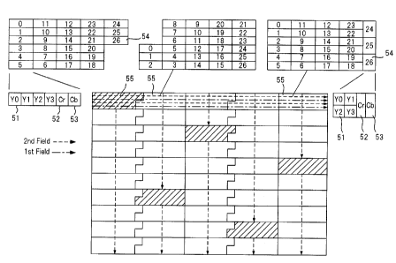
Referring to Fig.S, description will be made of how the
processing operations as above perform data reading and
writing when the external input video data is disordered.
Fig.5(a) shows a case where field discontinuity(the 1st
fields appearing in series ) occurs due to a scene connection
or the like. In Fig.5(a), since the first field of A2 is
detected by field detection after Writing of the first field
of Al, field discontinuity occurs so that the field error
flag is set and the page A to be written in and the page C
to be read out are retained. That is, the data of A2 is
overwritten on the page A on which only the first field data
CA 02362907 2001-08-13
32
of Al has been written in, and page retention is released
after the previous field error flag is reset so that the data
of A2 is read out and normalized video data is output.
Although not illustrated, when the second fields appear
in series, normalized video data is output by retaining
appropriate pages in the same manner.
Next, Fig.5(b) shows a case where the operation is
switched from the interlaced mode to the non-interlaced
mode(having the first fields only) . In Fig.5(b) , since the
first field of A2 is detected by field detection after writing
of the first field of A1, field discontinuity occurs so that
the field error flag is set and the page A to be written in
and the page C to be read out are retained.
However, since the first field of A3 is detected by field
detection after writing of the first field of A2 and the first
fields are successively detected downward, the field error
flag is kept up. The field discontinuity count is reset when
the field error flag is set up and counts up while both the
field error flag and the previous field error flag are up
so as to count how many times the field error has continued.
When the field error has continued for a predetermined number
of times ( four times in the figure ) , the non-inter flag is
set to generate a pseudo-field reallocating signal, whereby
the pseudo-first field and pseudo-second field of A7 are
written in. Thereafter, page retention is released so that
CA 02362907 2001-08-13
33
data B7 and the following data are seguentially written in
while A7 and the following are read out after readout of C0,
so that normalized video data is output.
The same operation is carried out for the non-interlaced
process for the secondfields only. Although not illustrated,
where the operation is switched from the non-interlaced mode
to the interlaced mode, the non-inter flag is reset when the
count of successive releasing of the field errors reaches
a predetermined number of times . Then the pages are retained
until the switching is completed, so that normalized video
data is output.
Next, Fig.S(c) shows a case where the number of lines
has varied (reduced). In Fig.5(c), the number of lines in
the first field of A1 is determined to be lower than the
predetermined value, so that the line count error flag is
set and the page A to be written in and page C to be read
out are retained. Data of A2 is written over the page A on
which data of A1 with an insufficient number of lines has
been written in, and page retention is released after the
reset of the previous field error flag so that data of A2
is read out . Thus , normalized video data is output . Though
not illustrated, when the number of lines has increased,
normalized video data will be output by retaining appropriate
pages in the same manner.
2 5 Next , Fig . 5 ( d ) shows a case of blank input . Blank input ,
CA 02362907 2001-08-13
34
which generally lacks input synchronizing signals, is
considered to be classified into three cases : the first case
where the vertical synchronizing signal does not come in,
the second case where the horizontal synchronizing signal
does not come in and the third case Where neither the vertical
synchronizing signal nor the horizontal synchronizing signal
comes in. Fig.5(d) shows the case Where the vertical
synchronizing signal does not come in. In Fig.5(d), the
vertical synchronizing signal stops coming in while the first
field of A1 is being Written in. In this case, however, the
horizontal synchronizing signal continues making its function,
so that the count of lines is determined to be greater than
the predetermined value . Therefore, the line count error flag
is set and the page A to be Written in and page C to be read
out is retained.
Then, the horizontal synchronization error flag Which
is given by logical OR between the line count error flag and
the horizontal synchronizing signal frequency error flag (not
shown) is set. Since the line count error flag is kept up
downward, the horizontal synchronization error flag also
remains being set. The horizontal synchronization error
count is reset when the horizontal synchronization error flag
is set and counts up while both the horizontal synchronization
error flag and the previous frame horizontal synchronization
error flag are up so as to count the number of times the
CA 02362907 2001-08-13
horizontal synchronization error has continued. When the
horizontal synchronization error has continued for a
predetermined number of times (four times in the figure),
the BLANK flag is set to mask the readout data with a black
5 mute signal, for example.
Although not shown, both the cases where no horizontal
synchronizing signal comes in and where neither vertical
synchronizing signal nor horizontal synchronizing signal
comes in are assumed as a case where no horizontal synchronizing
10 signal comes in. That is, when the horizontal synchronizing
signal stops coming in, the horizontal synchronizing signal
frequency error signal ( not shown ) is set so that the horizontal
synchronization error flag which is given by logical OR between
the line count error flag and the horizontal synchronizing
15 signal frequency error flag becomes set. Thereafter, the
operation is followed in the same manner as above by counting
the number of times the horizontal synchronization error has
continued. When the horizontal synchronization error has
continued for a predetermined number of times, the BLANK flag
20 is set to mask the readout data.
As has been described heretofore, video data can be
recorded based on the internal free-running synchronizing
signal when the vertical synchronizing signal in the external
input video data does not appear at the standard frequency
25 during recording and can be recorded based on the external
CA 02362907 2001-08-13
36
input synchronizing signal when it appears at the standard
frequency. It is also possible to perform switching between
the external input synchronizing signal and the internal
free-running synchronizing signal without causing any phase
jump. Further, use of a shuffling memory for three frames
makes it possible to avoid mixture of data within one frame,
and management of frame pages and forcible masking of video
data make it possible to output normal video data even if
the external input video data has been disordered.
Industrial Applicability
According to the present invention, use of a shuffling
memory for three frames as in the manner described above makes
it possible to perform normal recording by avoiding mixture
of frame data. Further, even if the synchronizing signal of
external input video data such as a composite signal etc.,
is disordered, the irregularity of the external input
synchronizing signal is detected so as to make management
of frame pages in the shuffling memory for three frames and
perform forced masking of video data, thus making it possible
to record normalized video data. Therefore, it is possible
to provide a recording and reproducing apparatus which is
improved in image quality in the recording mode.
Further, since the external input synchronizing signal
and the internal free-running synchronizing signal can be
CA 02362907 2001-08-13
37
switched smoothly, this enables accurate drum servo control
on the rotational rate of the recording head, thus leading
faithful recording of an input signal.