Note: Descriptions are shown in the official language in which they were submitted.
CA 02363336 2001-09-18
WO 00/59141 PCT/US00/08372
PREDISTORTION ARRANGEMENT USING MIXERS IN NONLINEAR
ELECTRO-OPTICAL APPLICATIONS
BACKGROUND OF THE INVENTION
The present invention relates generally to predistortion compensation in
nonlinear
electro-optical applications and, more particularly, to a predistortion
arrangement which
includes at least one mixer for producing second or higher order
intermodulation products
which are useful in distortion compensation. The invention is particularly
well suited for
production in integrated circuit form.
Nonlinear distortion is problematic in the use of nonlinear electro-optical
devices
such as, for example, lasers and modulators. One prior art approach, as
described in U.S.
patent number 4,992,754, issued to Blauvelt et al., relies on predistorting an
input signal in
an attempt to counteract the nonlinearity of the electro-optical device in a
way which is
intended to provide an overall linear transfer function. As described by the
'754 patent, prior
art techniques generally divide an input signal along two or more electrical
paths and
generate predistortion along one or more of the paths.
Figures 1 and 2 correspond to Figures 1 and 3, respectively, taken from the
'754
patent with reference numbers applied to the figures consistent with the
present description.
Figure 1 illustrates a prior art predistortion arrangement generally indicated
by the reference
number 10. Arrangement I0 includes input and output directional couplers 12a
and 12b,
respectively, a time delay circuit 16 in a signal path 18 and a distortion
path 20. The latter
includes a distortion generator 22, an amplitude adjust section 24, a
frequency tilt adjust
section 26 and a phase adjust section 28 arranged in series along distortion
path 20.
Referring to Figure 2, the '754 patent contemplates an implementation 30 of
the
block diagram of Figure 1, however, no provision is made for distortion
generator 22 (see
Figure 1). Implementation 30 does provide distortion path 20 including
amplitude adjust
section 24, frequency tilt adjust section 26 and phase adjust section 28 all
of which are
indicated within dashed lines. A detailed accounting of the components in
Figure 2 is not
necessary for reasons which will become evident, however, the presence of
certain
components should be noted. Specifically, a number of magnetic/inductive
components are
present. In particular, directional couplers 12a and 12b are normally
implemented using
CA 02363336 2001-09-18
WO 00/59141 PCT/US00/08372
transformers. Also, distortion path 20 includes a transformer 30 serving as a
signal splitter,
inductors L1 and L2 following frequency tilt adjust section 26 and a
transformer T2
connected to directional coupler 12b. As will be seen, the presence of these
inductive
components is considered to be particularly disadvantageous in accordance with
the
teachings of the present invention.
Referring to Figure 3, which corresponds to Figure 2 of the '754 patent having
reference numbers applied consistent with the present description, one
implementation of a
distortion amplifier (see item 22 in Figure 1 ) is illustrated in the form of
a push-push
amplifier generally indicated by reference number 32. Once again, it is of
interest here that
amplifier 32 includes aforementioned splitter transformer 30. It is submitted
that the specific
implementations used in the ' 754 patent, and in the prior art generally,
share at least one
disadvantage related to requirements for magnetic components which, in turn,
imposes
limitations on the adaptability of predistortion in compensating for the
nonlinearity of
electro-optical devices, as will be further described.
The present invention provides a highly advantageous drive arrangement
utilizing a
predistortion for driving nonlinear electro-optical devices in a heretofore
unseen manner
which resolves the foregoing limitations.
SUMMARY OF THE INVENTION
As will be described in more detail hereinafter, there is disclosed herein a
predistortion arrangement. This arrangement, like the prior art circuits
illustrated in Figures
1-3, develops predistortion for using an input signal to drive a nonlinear
device having a
drive input. However, the present invention includes first means for sampling
a portion of
the input signal. The sampled portion of the input signal is introduced to at
least one
predistortion path including a mixer responsive to the sampled portion of the
input signal for
producing at least second order intermodulation products of the input signal.
The second
order intermodulation products are then conditioned. Combining means then
combine the
conditioned second order intermodulation products with the sampled input
signal in a way
which produces a predistorted drive signal compensated for second order
distortion for use
in driving the drive input of the nonlinear device.
2
CA 02363336 2001-09-18
WO 00/59141 PCT/US00/08372
In one aspect of the invention, the sampling means and the combining means are
provided using resistive networks. In one feature, the use of the resistive
networks eliminates
the need for directional couplers incorporating magnetic components.
Accordingly, in one
feature, the predistortion arrangement including the mixer and the resistive
networks may be
provided in the form of an integrated circuit.
In another aspect of the invention, higher order intermodulation products may
be
generated using one or more additional predistortion paths. each of which
relies on the use of
mixers to generate the higher order intermodulation products.
BRIEF DESCRIPTION OF THE DRAWINGS
The present invention may be understood by reference to the following detailed
description taken in conjunction with the drawings briefly described below.
FIGURE I is block diagram of a predistortion circuit which is representative
of
Figure 1 from U.S. patent number 4,992,754, illustrating the overall design
including its use
of directional couplers.
FIGURE 2 is a schematic diagram of the circuit shown in Figure 1 and is
representative of Figure 3 from U.S. patent number 4,992,754, illustrating
again the use of
directional couplers as well as other magnetic components.
FIGURE 3 is a schematic diagram of a distortion amplifier which is
representative of
Figure 2 from U.S. patent number 4,992,754, shown here to illustrate the use
of a
transformer in the amplifier.
FIGURE 4 is a block diagram of a predistortion arrangement manufactured in
accordance with the present invention, shown here to illustrate the components
of the overall
arrangement.
FIGURE 5 is a schematic diagram of one embodiment of a second order products
path, manufactured in accordance with the present invention, which may form
part of the
arrangement of Figure 4, shown here to illustrate details of its construction.
CA 02363336 2001-09-18
WO 00/59141 PCT/US00/08372
DETAILED DESCRIPTION OF THE INVENTION
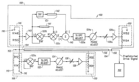
Having previously described Figures 1-3, attention is immediately directed to
Figure
4 which illustrates a predistortion arrangement manufactured in accordance
with the present
invention and generally indicated by the reference numeral 100 for use in
driving a nonlinear
electro-optical device 102 such as, for example, a laser diode or modulator.
Arrangement
100 includes an input 103 into which a suitable RF signal is fed. The signal
may comprise a
broad band signal for use in modulating the intensity of the output of the
particular nonlinear
electro-optical device 102 to be driven. As one example, a broad band signal
may comprise
television signals, in accordance with the NTSC standard. The overall
bandwidth of the
signal may be 860 MHz or more encompassing 128 or more NTSC signals. It is to
be
understood that the NTSC standard is used herein for exemplary purposes only
and that any
suitable signal format may be employed.
Predistortion arrangement 100 includes a fundamental signal path 104 and one
or
more predistortion paths. In the present example, a first predistortion path
is indicated within
a dashed line designated by the reference number 106 while a second
predistortion path is
indicated within another dashed line designated by the reference number 108.
The first
predistortion path generates intermodulation products of the second order
while the second
predistortion path generates intermodulation products of the third order.
Therefore, first
predistortion path 106 may be referred to as a second order products path
while second
predistortion path 108 may be referred to as a third order products path. The
first
predistortion path will be discussed in detail immediately hereinafter.
Still referring to Figure 4, first predistortion path 106 includes a resistive
voltage
divider network 110 indicated within a dashed line made up of resistors Rl 12
and 8114
connected from fundamental signal path 104 in series to a ground 116. An
attenuated signal
is taken from the junction of resistors 8112 and 8114 and provided to the
Local Oscillator
(hereinafter LO) input of a mixer 120a. At the same time, the attenuated
signal is also
provided to the Radio Frequency (hereinafter RF) input of mixer 120a. In
accordance with
the present invention, mixer 120a functions in a broad band manner to generate
second order
intermodulation products at the Intermediate Frequency (hereinafter IF)
output. Presently, it
is preferred to use a double balanced active mixer as mixer 120 for reasons
including high
LO-IF isolation, and RF-IF isolation . In a preferred embodiment, a Gilbert
cell design is
utilized such as is incorporated in the IAM-81008 mixer which is available
from Hewlett-
Packard. A double balanced active mixer design includes characteristics of
high gain and
4
CA 02363336 2001-09-18
WO 00/59141 PCT/US00/08372
relatively high isolation between the IF output and RF and/or LO inputs.
Irrespective of the
specific mixer which is used, it is important to note that the present
application requires the
ability to produce intermodulation products corresponding to a broad
bandwidth. Therefore,
the use of mixer 120a in this application causes concerns to arise which are
not present in
frequency limited applications such as that of doubling of a particular
frequency. These
concerns include bandwidth capabilities of the mixer as well as the phase
linearity of the
mixer. It is to be understood that any mixer design, either currently
available or to be
developed, is contemplated for use herein so long as the requisite
characteristics are
provided.
Second order intermodulation products produced at the IF output of mixer 120a
are
passed to a series of compensation sections which prepare the second order
intermodulation
products for proper combination with the fundamental signal. Initially, the
second order
intermodulation products are provided to a slope adjust section 122 which
compensates for
amplitude variations occurring with respect to frequency change. Following
slope adjust
compensation, the second order intermodulation products enter a phase adjust
compensation
section 124 and, thereafter, pass through an amplitude compensation section
126 which is
followed by an amplifier 128. It should be noted that amplifier 128 is
considered as optional
for reasons to be explained at an appropriate point below. It is noted that
the compensation
sections may be arranged in a different order than that illustrated. A
specific implementation
of the compensation sections will be described below.
Continuing to refer to Figure 4, the second order intermodulation products are
then
provided to an output resistive network 130 indicated within a dashed line and
including
resistors 8132 and 8134. The second order intermodulation products are coupled
into a
delay line 136 on the fundamental signal path. The purpose of delay line 136
is to introduce
a delay along the fundamental signal path which matches the delay of the
second order
products along first predistortion path 106. Figure 4 illustrates connection
of output resistive
network 130 in a tapped manner to the overall delay line 136. Such a tapped
delay line may
be provided, for example. using a microstrip line formed on a printed circuit
board. As
illustrated, the line may be tapped so as to provide further delay for another
portion of the
circuitry.
Still referring to Figure 4, third order distortion products path 106 is
similar to the
second order path with the addition of a number of components. Specifically,
the additional
5
CA 02363336 2001-09-18
WO 00/59141 PCT/US00/08372
components include delay lines 141 and 142, an amplifier 143, an attenuator
144, a summing
section 145 and another mixer. It is noted that all of the mixers used herein
may include the
same part number and, therefore, have been identified with the common
reference number
120, but with a different letter appended to this common reference number for
purposes of
clarity. Therefore, the mixers in the third order path have been identified
using the reference
numbers 120b and 120c. An input resistive network 146 within a dashed line
includes
resistors 8148 and 8150 and provides a portion of the overall input signal to
amplifier 143.
The amplified portion of the input signal is then fed to mixer 120b which
produces second
order intermodulation products in the same manner as mixer 120a, described
above, by
providing the same input signal to the RF and LO inputs of the mixer. The
second order
intermodulation products produced at the IF output of mixer 120b are then fed
to the RF
input of mixer 120c. The latter also receives, at its LO input, the amplified
portion of the
input signal delayed by delay line 141. Delay line 141 includes an electrical
length matching
the electrical length of mixer 120b so that the signal arrives at mixer 120c
with the proper
phase.
Using the second order products and the delayed amplified portion of the input
signal, mixer 120c generates third order intermodulation products at its IF
output. Once
again, it is important to understand that third order products should be
produced
corresponding to the entire bandwidth of the fundamental signal. In this
regard, the concerns
discussed above with regard to the use of mixer 120a in the second order
products path are
of even more concern since the required bandwidth and phase linearity are more
difficult to
achieve with the cascade of two mixers than with the single mixer used for
generating
second order products . The third order intermodulation products are then
received by the
non-inverting input, (+), of summing section 145. Further suppression of the
fundamental
signal is achieved by using attenuator 144 and delay line 142 in cooperation
with summing
section 145, serving as a fundamental cancellation network I ~ 1. The need for
fundamental
cancellation using attenuator 144, delay line 142 and summing section 145 will
be addressed
at an appropriate point below. For the moment, it should be mentioned that the
present
invention contemplates provisions for fundamental cancellation in any suitable
manner in the
third order products path. Moreover, it is noted that the implementation of
summing section
145, attenuator 144 and delay line 142, for example, in the form of a
microstrip line, is
considered to be within the skill of one of ordinary skill in the art.
6
CA 02363336 2001-09-18
WO 00/59141 PCT/US00/08372
During the operation of the third order products path, attenuator 144 receives
a
portion of the fundamental signal and reduces its level to an appropriate
attenuated value.
The attenuated fundamental signal is then delayed by delay line 142 which is
configured to
match the delay encountered by the fundamental signal and accountable to
mixers I20b and
120c in producing the third order products. The attenuated fundamental signal
is provided to
an inverting input, (-), of summing section 145. With an appropriate level of
the fundamental
signal present in the summing section, the fundamental or base band signal is
substantially
canceled so as to avoid a significant interaction with nonlinearities in the
compensation
sections which follow on the third order products path.
Still describing the third order products path, the compensation sections in
the third
order products path are functionally equivalent to the series of compensation
sections
included in the second order distortion path and, therefore, are designated
using identical
reference numbers with the letter "a" appended thereto. Accordingly, these
compensation
sections are indicated as slope adjust section 122a, phase adjust compensation
section 124a
and amplitude compensation section 126a, which are followed by an amplifier
128a. As
mentioned above with regard to amplifier 128, amplifier 128a is considered as
being
optional. It is to be understood that design details of these compensation
sections within the
third order products path may differ with regard to corresponding sections in
the second
order products path, for example, due to the need to compensate for the
additional
components in the third order path and the differences between the second and
the third
order distortion produced in the nonlinear device to be predistorted. It
should also be
understood that the present invention contemplates using other products paths
to produce
higher order (i.e., greater than third order) products by adding mixers, for
example, to third
order path 108 of Figure 3.
From amplifier 128a, the third order products are provided to an output
resistive
network 150 comprised of resistors 8152 and 8154 which introduces the third
order
products back onto the fundamental signal line for combining with the
fundamental signal
and with the second order products at a point 156 following delay line 136. It
is noted that
the delay introduced between the tap at which the second order products are
introduced to
the fundamental signal path and point 156 may be in the form of a separate
delay line having
an appropriated lumped value. The final predistorted drive signal is then
provided to non-
linear electro-optical device 102.
7
CA 02363336 2001-09-18
WO 00/59141 PCT/US00/08372
Having generally described the structure of predistortion arrangement 100,
attention
is now directed to specific details of its operation with attendant
advantages. First
considering second order predistortion path 104, it should be appreciated that
mixer 120, as
specified, provides significant levels of isolation of the fundamental signal
in the
compensation section of the path. That is, mixer 120a reduces the level of the
fundamental
signal at its IF output to a level at least 20 dB below the level of the
second order
intermodulation products. It is recognized herein that this reduction in the
fundamental
signal is attributable to the fourier transform of the square of the
fundamental signal having
only second order terms and a DC term, which is easily eliminated, and the
high RF-IF and
LO-IF isolation of the mixer. As one advantage associated with this low
fundamental level,
any of the various functional blocks along the second order products path
i.e., slope adjust
section 122, phase adjust section 124 and amplitude adjust section 126, may be
permitted to
exhibit some degree of nonlinearity above levels which would normally be
considered as
being acceptable, since the overall effect of such nonlinearity is directly
dependent upon the
level of the fundamental signal with which it is interacting. That is, the
lower the
fundamental signal, the more nonlinearity may be permitted. One advantage of
the present
invention, therefore, is the ability to use lower cost components in the
compensation
sections. Another advantage, when implementing a voltage controlled
compensation circuit,
is the ability to reduce current consumption of the compensation network.
Referring to Figures 1 and 4, the directional couplers shown in Figure 1
provide the
following functions: ( 1 ) they efficiently sample and inject signal; (2)
coupler 12a isolates
the device to be predistorted from distortion reflected from the distortion
generator (item 22
in Figure 1); and (3) coupler 12b isolates the distortion compensation network
(items 24, 26,
28 in Figure 1 ) from the fundamental signal. This is important for reasons
described
previously. All of these functions can be performed by resistive sputters and
combiners if
extra gain is provided in the distortion path. Active mixer 120a in Figure 4,
such as a Gilbert
cell, is highly desirable for providing this extra gain. Moreover, if
additional isolation of the
distortion compensation network is desired, amplifier 128 may be added and
8132 adjusted.
This may be necessary if a high level of second order predistortion is
required, if the
distortion compensation network has too much loss, or if highly nonlinear
components are
used in the distortion compensation network.
CA 02363336 2001-09-18
WO 00/59141 PCT/US00/08372
Still considering second order predistortion path 104, it should be
appreciated that the
combination of mixer 120 with input resistive network 110 and, in fact, with
output resistive
network 130 is highly advantageous. The use of output resistive network 130 is
facilitated as
a result of the gain of mixer 120a. Inherently, the resistive networks
advantageously provide
no frequency dependent attenuation which would serve to reduce bandwidth. It
should be
appreciated that amplifier 128 is considered as optional in view of specific
values chosen for
8132 and 8134. That is, if the value of 8132 is great enough, leakage of the
fundamental
signal into the compensation sections has been found to be at an acceptable
level without the
need for amplifier 128. This holds even in instances where more significant
levels of
nonlinearity are permitted in the compensation section, as described above.
Still further
advantages associated with the combination of mixer 120a and the resistive
networks will be
described.
With continuing reference to Figure 4, attention is again directed to third
order
products path 108. While the fundamental signal is suppressed to a level
significantly below
that of the second order products produced by mixer 120b , this level of
suppression is not
possible in the products of mixer 120c. The output of mixer 120c is the cube
of the
fundamental signal. The Fourier transform of the cube of the fundamental has
9.SdB more
power in the fundamental than in the desired third order products. Therefore,
further
suppression of the fundamental signal is desirable. Fundamental cancellation
network 151
has been found to be suitable in this application not only for the reason that
sufficient
cancellation is achieved, but also since the use of magnetic components (i.e.,
inductors) is
avoided, as will be further discussed. Moreover, with the addition of
fundamental
cancellation network 151, it is considered that the third order products path
shares the
advantages of the second order products path. For as example, if the value of
8154 is great
enough, leakage of the fundamental signal into the third order path
compensation sections
has been found to be at an acceptable level without the need for amplifier
128a. However,
the values of 8152 and 8154 may be adjusted in view of isolation, and gain
provided in the
presence of amplifier 128a as described above with regard to amplifier 128.
Referring to Figures 1 and 2, the reader is reminded of the discussions above
relating
to the '754 patent. The latter utilizes directional couplers 12a and 12b which
do provide
isolation of the fundamental signal. At first appearance, therefore, the use
of directional
couplers seems advantageous since isolation is provided. However, in
accordance with the
present invention, the use of directional couplers is considered to be
unacceptable for a
9
CA 02363336 2001-09-18
WO 00/59141 PCT/US00/08372
number of reasons, irrespective of isolation provided thereby. One reason for
which it is
desirable to avoid the use of directional couplers resides in their cost. The
resistive networks
used herein are insignificant in cost as compared with directional couplers.
An even more
compelling reason for using the configuration disclosed by the present
invention will be
described immediately hereinafter.
Referring to Figures 1, 2 and 4, as mentioned previously, directional couplers
12a
and 12b (Figures I and 2) are typically implemented using magnetic components.
The
present invention recognizes that the use of these components is particularly
disadvantageous since present technologies are incapable of providing such
magnetic
components as part of an overall integrated circuit. That is, if a
predistortion circuit is to be
provided in the compact form of an integrated circuit, the need for
directional couplers
should be eliminated. The predistortion arrangement of the present invention,
as depicted in
Figure 4, serves this purpose. The combination of mixer 120 with the input and
output
resistive networks is readily provided in integrated circuit form. Moreover,
predistortion
arrangement 100 has also eliminated the need for other inductive components
such as the
transformers which are used in the predistortion path of the '754 patent while
providing still
further advantages through the manner in which the compensation circuitry is
implemented
along the predistortion path.
Attention is now directed to Figure 5 which illustrates one embodiment of a
predistortion arrangement for generating second order products which is
manufactured in
accordance with the present invention and generally indicated by the reference
number 170.
For purposes of clarity, reference numbers corresponding to like components in
Figure 4 will
be used whenever possible. Second order intermodulation products path 106 is
indicated and
forms part of drive arrangement 170. During operation, the fundamental signal
enters the
predistortion path at a junction 180 of capacitor C182 and resistor 8184.
Capacitors C182
and C186 block DC from either end of delay line 136. Input resistive network
110 sends
most of the fundamental signal through adjustable delay line 136 along primary
path 104,
however, a small amount of the fundamental signal is coupled into the RF (pin
no. 4) and LO
(pin no. 5) ports of Gilbert cell mixer 120a by resistors 8184, 8188, and
8190. These latter
resistors are preferably selected to drive the RF port of the mixer harder
than the LO port
since the LO port is buffered internal to the mixer. It is noted that the
configuration of input
resistive network 110 varies slightly from its configuration in Figure 4. Such
modifications
are considered as within the scope of the present invention. C 192, C I 94 and
C 196 are DC
CA 02363336 2001-09-18
WO 00/59141 PCT/US00/08372
blocking capacitors for the RF, LO, and IF (pin no. I ) ports of Gilbert mixer
120a. C 198
and C200 provide a suitable RF ground below SOMHz. Second order
intermodulation
products are produced at the IF output of mixer 120a (pin no. I ).
Still referring to Figure 5, the second order products then pass through phase
adjust
section 124, slope adjust section 122 and amplitude adjust section 126. Phase
adjust section
includes varactors D202a and D202b. Resistors 8204, 8206, 8208 and 8210 are
needed to
bias the varactors in both phase adjust section 124 and slope adjust section
122. An external
phase control voltage is provided on a line 212. The control voltage is
coupled through 8214
and filtered by capacitors C216 and C21.8. Slope adjust section 122 includes
varactors
D220a and D220b. An external slope adjust signal is provided on a line 222 and
is filtered
by resistor 8224 cooperating with capacitors C226 and C228. Capacitor C230
serves as a
DC block and couples the second order products signal to amplitude adjust
section 126.
Continuing with a description of predistortion arrangement 170, the amplitude
of the
second order products is adjusted using a pin diode attenuator including PIN
diodes D232a
and D232b that are biased by a resistor 8233. Note that amplifier 128 (Figure
2) is not used
here. An external amplitude control voltage is provided on a line 234 via
resistor 8236 and
capacitor C238 for biasing the PIN diodes. Capacitor C240 couples the second
order
products to output resistive network 130 which is made up of resistors 8242
and 8244. As
mentioned above and in this example, the gain of mixer 120a allows use of a
relatively large
resistance for 8242 in the absence of amplifier 128 (Figure 4) for limiting
the leakage of the
fundamental signal in the reverse direction into the compensation sections.
Thus, the second
order products are combined with the fundamental signal at a point 246 along
primary path
104 following delay line 136.
Having described predistortion arrangement 170, it should be mentioned that
the
phase, slope and amplitude adjustments provided thereby are somewhat
interactive.
However, it should be appreciated that implementation of the circuit in a way
which
provides for an external control voltage for each section is highly
advantageous since
computer control is readily providable to these control lines. At the same
time, as a result of
the high isolation performance provided by mixer 120a, this external control
configuration
overcomes the difficulty inherent in the introduction of nonlinearity
exhibited by the
varactor diodes.
11
CA 02363336 2001-09-18
WO 00/59141 PCT/US00/08372
Referring to Figures 4 and 5, while predistortion arrangement 170 has been
implemented using discrete components, it is to be understood that the
entirety of the
arrangement, with the present exception of delay line 136, may be provided in
the form of an
integrated circuit. The latter may include a configuration which is different
from the specific
configuration shown in Figure 5 so long as equivalent functionality is
achieved. Moreover,
the present invention contemplates providing the entirety of predistortion
arrangement 100
(Figure 4), with the possible exception of its delay lines, in the form of an
integrated circuit.
In this regard, as described above, such integration is accomplished through
the elimination
of inductive components by using mixers in combination with resistive networks
in the
highly advantageous manner described above. Delay lines may be provided, for
example, in
the form of microstrip lines arranged in proximity to a predistortion
integrated circuit that is
manufactured in accordance with the present invention or by a coaxial cable.
Since the predistortion arrangement disclosed herein may be provided in a
variety of
different configurations. it should be understood that the present invention
may be embodied
in many other specific ways without departing from the spirit or scope of the
invention.
Therefore, the present examples and methods are to be considered as herein,
but may be
modified within the scope of the appended claims.
12