Note: Descriptions are shown in the official language in which they were submitted.
CA 02363422 2001-09-18
[PCT/EP00/02479]
METHOD FOR COMPENSATING FOR THE DISPERSION OF CO-TRANSMITTED
OPTICAL SIGNALS HAVING DIFFERENT WAVELENGTHS
The present invention is directed to the field of dispersion
compensation as applied to co-transmitted optical signals
having different wavelengths, in optical communications
networks.
In optical communications networks set up in known methods
heretofore, one installed, almost exclusively, standard
single-mode fibers having an attenuation of about 0.4 dB/km
and a dispersion minimum at 1310 nm.
To an increasing degree, the wavelength range of around 1550
nm is used for optical communications. This is due to the
lower attenuation of approximately 0.2 dB/km, the increasing
use of wavelength division-multiplex transmission, and the
availability of a virtually perfected optical-fiber light
amplifier, the EDFA (erbium doped fiber amplifier), which can
be used to amplify several channels simultaneously within a
broad range of around 1550 nm.
One deficiency of the above approach is that the transmission
bandwidth and the amplifier distances are limited by the high
dispersion of standard single-mode fibers of about 17 ps/nm x
km at 1550 nm. Therefore, for longer transmission routes and
bandwidths in the Gb/s range, it is necessary to install
dispersion-compensating elements.
It is generally known to use dispersion-compensating fibers
(DCF) which exhibit a high negative dispersion. -100ps/nm x km
is given as a typical value for the dispersion of a DCF.
Accordingly, 17 km of DCF are needed to compensate for the
dispersion of a 100 km long standard single-mode fiber. The
NY01 397580 v 1
CA 02363422 2001-09-18
compensation fibers are wound onto spools, which must be at
least 10 cm in diameter to avoid loss of curvature. There are
several drawbacks associated with using a
dispersion-compensating fiber DCF for dispersion compensation:
- A substantial length of a relatively expensive, special
fiber is needed.
- The fiber spool has large dimensions. This can lead to
problems in line repeater stations or in cable jointing
chambers, particularly when working with multi-core
optical cables.
- A supplementary attenuation is added. Due to their
special core structure, dispersion-compensating fibers
exhibit an attenuation of about 0.5 dB/km, i.e., a fiber
length of 17 km yields an attenuation of about 9dB.
The above described properties and possible applications of
dispersion-compensating fibers DCF, as well as the wavelength
division-multiplex transmission and optical-fiber light
amplifiers are described in detail in "Optische
Telekommunikationssysteme" [Optical Telecommunications
Systems] by H. Hultzsch, Damm Publishers, Gelsenkirchen (1996)
p. 123 and pp. 296-298.
Another dispersion compensation method is based on the use of
optical fiber gratings (see likewise in "Optische
Telekommunikationssysteme" [Optical Telecommunications
Systems] by H. Hultzsch, Damm Publishers, Gelsenkirchen (1996)
pp. 152 - 153). However, optical fiber gratings of about one
meter length are required to compensate for dispersion over
broad wavelength ranges, e.g., the EDFA range of 1530 nm -
1570 nm. The manufacturing of very long optical fiber gratings
having the necessary tolerances with respect to the grating
constants and the requisite long-term stability is expensive
NY01 397580 v 1 2
CA 02363422 2001-09-18
and is still in the development stage.
The technical objective of the present invention is directed
to an economical approach that requires little overall space
to compensate for the dispersion of co-transmitted optical
signals having different wavelengths 1~.
The achievement of the objective in accordance with the
present invention is based on the use of photonic crystals.
Photonic crystals are periodic arrays of dielectric materials
having high and low dielectric constants, alternately disposed
as one-, two-, or three-dimensional gratings having periods of
A/3 and rod or cubic diameters of A/6. See J. D. Joannopoulus
et al.: Photonic Crystals: Molding the Flow of Light, ISBN
0-691-03744-2 (1995).
In accordance with the present invention, co-transmitted
optical signals of different wavelengths which, after
propagating through a line section, exhibit dispersion-induced
transit-time differences, are coupled via an optical fiber
input E into an arrangement configured as a network, which is
made up of photonic crystals Kl through Kn positioned one
after another on an optical waveguide 2. Photonic crystals Kl
through Kn are, therefore, optically connected to one another.
Photonic crystals K1 through Kn are formed in such a way that
they reflect or divert signals of a specific wavelength and
allow signals having other wavelengths to pass through,
unattenuated. For example, the formation of first photonic
crystal K1 is such that it exclusively reflects the signals of
a first wavelength. Optical signals of other wavelengths pass
through photonic crystal K1, unattenuated, and are coupled
into the downstream photonic crystal K2. Of those signals
transmitted through first photonic crystal K1, the subsequent,
second photonic crystal K2 reflects, in turn, only those
signals having a second wavelength. It likewise permits the
signals having other wavelengths to pass through. In
accordance with this principle, the signal continues to be
NY01 397580 v 1 3
CA 02363422 2001-09-18
passed on by a photonic crystal to a further photonic crystal
until the signals of all wavelengths have been reflected by
photonic crystals K1 through Kn assigned to them.
Since the positive dispersion value of the signals coupled
into the optical fiber input is known for the individual
wavelengths, path lengths, which are afflicted by negative
dispersion in the array made up of successively ordered
photonic crystals K1 through Kn, are defined in accordance
with the individual wavelengths, are dimensionally designed to
alter or completely cancel the dispersion differences of the
signals of the individual wavelengths. Before the signal of a
defined wavelength is reflected in one of the successively
ordered photonic crystals K1-Kn, it has already traveled a
path length up to the element reflecting the defined
wavelength in the photonic crystal and acted upon by such a
negative dispersion. This path length is defined by the
distance between optical fiber input E and the reflecting
mirror in photonic crystal K1 through Kn in question.
The dispersion-compensated signals of different wavelengths
reflected by the photonic crystals are again coupled into a
shared optical fiber output A to be retransmitted by a
suitable module, such as an optical circulator 1.
The method of the present invention shall now be explained in
greater detail on the basis of five exemplary embodiments.
Assuming the case where optical signals transmitted with
different wavelengths Vii, e.g. , three wavelengths lei, ~i+1, Ai,z.
exhibit dispersion-induced transit-time differences after
propagating through a line section, the specific embodiments
are especially directed to once again compensating for these
transit-time differences. However, these approaches also
include the option of setting a predistortion including
defined transit-time differences for the signals of the
individual wavelengths, for example for the wavelengths lei,
NY01 397580 v 1 4
~i+1 ~ ~i+2
CA 02363422 2001-09-18
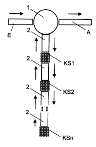
Figure 1 depicts an arrangement for compensating for
dispersion, where the optical signals afflicted by
transit-time differences are coupled via a shared optical
fiber input E into an optical circulator 1. The optical
signals afflicted by transit-time differences are coupled by
optical circulator 1 into a module made up of photonic
crystals KSl through KSn which are disposed one after another
as selective reflection filters on a waveguide 2.
In this context, each of photonic crystals KS1 through KSn is
tuned to only reflect the signals having a specific wavelength
of those signals coupled in via optical circulator 1, but to
allow the signals of the other wavelengths to pass through. It
is the actual transit-time difference of the signals of the
particular wavelength that determines which photonic crystal
KS1 through KSn is designed as a reflection filter for which
wavelength. The greater the transit-time difference is, the
longer the optical path must also be that the signal needs to
travel until complete dispersion compensation is attained.
This path can be precisely calculated. In one exemplary
embodiment including, for example, three different
wavelengths, this would signify that photonic crystal KS1 only
reflects the signals of wavelength 1~i to optical circulator 1.
The light of wavelengths Ai+~. 1~i+2 is transmitted through
photonic crystal KS1, unattenuated, to photonic crystal KS2.
Photonic crystal KS2 is tuned to only reflect the signals of
wavelength ~i+1. The signals of wavelength 1~i+2 pass through,
unattenuated, to photonic crystal KS3. Photonic crystal KS3 is
tuned to only reflect the signals of wavelength 1~i+2.
Consequently, all signals coupled in via optical circulator 1
are re-reflected to optical circular 1. The now
dispersion-compensated signals having the three wavelengths ?~i,
~i+~, and Ai+2 are again coupled by optical circulator 1 into
the shared, optical fiber output A, and retransmitted via
NY01 397580 v 1 5
CA 02363422 2001-09-18
appropriate downstream devices.
Figure 2 illustrates the transmission as a function of the
wavelength for the three photonic crystals KS1-KS3 designed as
selective reflection filters.
The specific embodiment pictured in Figure 3 differs from the
approach according to Figure 1 in that tunable dispersion
shifters NLO1-NLOn are additionally interposed in waveguides 2
between photonic crystals KS1-KSn designed as selective
reflection filters. The tunable dispersion shifters NLO1-NLOn
make further dispersion compensation possible in addition to
the fixed path distances encumbered by negative dispersion. In
this context, dispersion shifters NLOl-NLOn are preferably
tuned to enable the sum of fixed and adjustable dispersion
shifting to compensate for the dispersion differences among
the individual wavelengths.
The dispersion-compensating arrangement reproduced in Figure 4
is directed to a specific embodiment that functions without
optical circulator 1. In this example, photonic crystals KD1
through KDn are tuned to deflect signals of a particular
wavelength. Photonic crystals KD1 through KDn, which are
successively ordered on waveguide 2, are specifically designed
as drop filters, which laterally deflect optical signals of a
desired wavelength out of waveguide 2 and allow optical
signals of other wavelengths to pass through to the downstream
photonic crystal. The signals, which are filtered out
laterally in dependence upon their wavelength by photonic
crystals KD1 through KDn designed as drop filters, are
optically transmitted via waveguide sections to photonic
crystals KAl through KAn designed as adders and are mutually
coupled again via optical fiber output A to be further
transmitted. The described arrangement eliminates the need for
optical circulator 1 that is still required in the first
exemplary embodiment. The signals of the various wavelengths
are again present, without transit-time differences, at the
NY01 397580 v 1 6
CA 02363422 2001-09-18
output of photonic crystal KA1 designed as an adder. The
dispersion-compensation arrangement pictured in Figure 4,
_ including photonic crystals KD1 through KDn designed as drop
filters and photonic crystals KA1 through KAn designed as
adders, is set up to compensate for the dispersion of the
signals of the various wavelengths, in accordance with the
dispersion to be expected at suitable geometric distances 3.
In this instance, the arrangement is set up to include
variable transmission (wavelength 1 through wavelength n),
which is selected on the basis of the design and the period
intervals of waveguides 2. Waveguides 2 are interrupted by
regions in which the signals are coupled out of photonic
crystals KD1-KDn in dependence upon their wavelength lei, due to
the geometry of the three-terminal region, and are coupled
again into the corresponding photonic crystals KA1-KAn
designed as adders, and are summed. All signals are then
coupled again into optical fiber output A. In this manner, the
transit-time displacement caused by dispersion is compensated
for all signals. It is necessary to manufacture and install
specially adapted components for the various paths of the
network, as is the case in all dispersion-compensation
techniques. A certain standardization can be achieved, for
example, also by employing standardized distances between the
stations where the dispersion compensation is carried out.
Figure 5 shows an arrangement which essentially corresponds to
that of Figure 4. This arrangement is likewise made up of
optical fiber input E, of photonic crystals KDl through KDn
designed as drop filters and configured on waveguide 2, of
photonic crystals KA1-KAn designed as adders, and of the
shared optical fiber output A.
Additionally situated on the optical paths between the
deflecting outputs of photonic components KD1 through KDn
designed as drop filters and the inputs of the photonic
components KA1 through Kan designed as adders are dispersion
shifters NLO1 through NLOn, whose dispersion-shifting effect
NY01 397580 v 1 7
CA 02363422 2001-09-18
is able to be individually tuned for each wavelength before
the signal is fed back via photonic crystals KA1 through KAn,
designed as adders, into shared optical fiber output A. The
desired dispersion is set by applying different voltages at
dispersion shifters NLO1-NLOn or through the action of other
physical parameters, such as temperature, magnetic field, etc.
In the process, dispersion shifters NLO1-NLOn can be loaded
with one or a plurality of voltages and be made of a plurality
of nonlinear optical materials. Dispersion shifters NLO1
through NLOn are preferably connected via planar waveguides 4,
or also via photonic crystal waveguides, in each case to
photonic crystals KA1 through KAn assigned to them as adders.
By selecting appropriate materials and rating the voltage for
the individual wavelengths, one can roughly or even finely
tune the desired additional dispersion. Nonlinear optical
elements NLO of this kind make it possible for the set-up
according to Figure 5 to be adapted within certain limits to
the particular conditions of the application. Thus, an
arrangement in accordance with Figure 5 has universal
applicability. Non-linear, optical dispersion shifters
NLO1-NLOn can be made, for example, of photonic crystal
structures which are filled with liquid crystals. Also
conceivable is the use of crystal rod or hole structures
filled with non-linear, optical polymers. These structure are
constructed in an electrical field that is tuned as a function
of the required, non-linear optical dispersion shifting. In
this context, the specific, optically non-linear dispersion
shift is determined as a function of the compensation path
length for the individual wavelengths.
If dispersion shifters NLO1 through NLOn are optically
inserted between photonic crystals KD1-KDn, formed as drop
elements, and photonic crystals KA1 through KAn functioning as
adders, then the tuning is carried out separately for each
wavelength. Therefore, this arrangement makes it possible to
individually adjust the required dispersion shift for each
individual wavelength.
NY01 397580 v 1 8
CA 02363422 2001-09-18
Alternatively, in another advantageous specific embodiment in
accordance with Figure 6, dispersion shifters NLO1 through
NLOn can be positioned in the optical path (waveguide 2)
between the individual photonic crystals KD1-KDn designed as
drop filters. In this case, dispersion shifters NLO1-NLOn act
on different wavelengths simultaneously. The action of
dispersion shifters NLO1 through NLOn adds up in the process
for the various wavelengths from dispersion shifter to
dispersion shifter. The signals are fed back again via the
waveguides between photonic crystals KD1-KDn designed as drop
filters and photonic crystals KA1-KAn designed as adders,
which sum up the signals and feed them back again into optical
fiber output A.
The approach of the present invention makes it possible to
assemble high-quality, photonic-crystal add-drop filters,
which are approximately 1000 times shorter than conventional
diffraction gratings that are configured as chirped gratings
at a length of approximately 100 cm. The approach of the
present invention makes it possible to construct a
dispersion-compensation arrangement that is accommodated on a
chip of a few centimeters in size. This chip component has the
advantage of a greater temperature stability, so that it can
also be used for larger temperature ranges. In addition, in
the specific embodiments according to Figures 4, 5, and 6, the
need is eliminated for cost-intensive circulator 2. Besides
improving operation, the present invention provides a much
more economical approach than one based on the known,
conventional structures. The electrically tunable dispersion
shifters NLO1 through NLOn make it possible to adapt the
approach on an individual basis to the particular
requirements, even given different path lengths.
Solid-state waveguide technology can be used to implement the
practical design of the dispersion-compensation arrangement of
the present invention by employing three-dimensional additive
lithography or electrolytic, light-supported etching of
NY01 397580 v 1 9
CA 02363422 2001-09-18
silicon, including appropriate patterning of the apertured
mask.
NY01 397580 v 1 10
CA 02363422 2001-09-18
Table of Reference Numerals
E optical fiber input
A optical fiber output
1 optical circulator
2 waveguides
3 geometric distances between the photonic crystals
4 planar waveguides
K1-Kn photonic crystals
KS1-KSn photonic crystals designed as selective reflection
filters
KD1-KDn photonic crystals designed as drop elements
KA1-KAn photonic crystals designed as adders
NLO1-NL04 dispersion shifters
?~ wavelength
NY01 397580 v 1 11