Note: Descriptions are shown in the official language in which they were submitted.
CA 02363609 2001-11-20
Doc. No. 10-425 CA(2) Patent
CONTROL SYSTEM FOR OPTICAL CROSS-CONNECT SWITCHES
MICROFICHE APPENDIX
[0001 ] Not Applicable.
TECHNICAL FIELD
[0002] The present invention relates to optical cross-connect switches, and in
particular to a
control system for an optical cross connect capable of detecting and
correcting mirror positioning
errors within the optical cross-connect.
BACKGROUND OF THE INVENTION
[0003] Optical matrix cross-connects (or switches) are commonly used in
communications
systems for transmitting voice, video and data signals. Generally, optical
matrix cross-connects
include multiple input and/or output ports and have the ability to connect,
for purposes of signal
transfer, any input port/output port combination, and preferably, for N x M
switching applications,
allow for multiple connections at one time. At each port, optical signals are
transmitted and/or
received via an end of an optical waveguide. The waveguide ends of the input
and output ports are
optically connected across a switch core. In this regard, for example, the
input and output waveguide
ends can be physically located on opposite sides of a switch core for direct
or folded optical path
communication therebetween, in side-by-side matrices on the same physical side
of a switch core
facing a mirror, or they may be interspersed in a single matrix arrangement
facing a mirror.
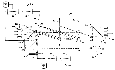
[0004] Establishing a connection between an input port and a selected output
port involves
configuring an optical path across the switch core. One known way to configure
the optical path
involves the use of one or more movable mirrors interposed between the input
and output ports. In
this case, the waveguide ends remain stationary and the mirrors are used to
deflect a light beam
propagating through the switch core from the input port to effect the desired
switching.
Micro-electro-mechanical mirrors known in the art can allow for one- or two-
dimensional targeting to
optically connect any input port to any output port. For example, United
States Patents Nos.
5,914,801, entitled MICROELECTROMECHANICAL DEVICES INCLUDING ROTATING
PLATES AND RELATED METHODS, which issued to Dhuler et al on June 22, 1999;
6,087,747,
entitled MICROELECTROMECHANICAL BEAM FOR ALLOWING A PLATE TO ROTATE IN
RELATION TO A FRAME IN A MICROELECTROMECHANICAL DEVICE, which issued to
Dhuler et al on July 11, 2000; and 6,134,042, entitled REFLECTIVE MEMS
ACTUATOR WITH A
LASER, which issued to Dhuler et al on October 17, 2000, disclose micro-
electro-mechanical mirrors
that can be controllably moved in two dimensions to effect optical switching.
1
CA 02363609 2001-11-20
Doc. No. 10-425 CA(2) Patent
[0005] One of the major challenges of designing an optical cross-connect (OXC)
switch using
tiltable Micro-Electro-Mechanical Switch (MEMS) mirrors is the need to
accurately control each of
the mirrors so that low fiber-to-fiber losses can be maintained over the
operation lifetime of the
switch. The major obstacle to creating an optical switch is the necessary
control for precisely
addressing each of the mirrors to achieve accurate switching with low loss.
Small errors in angle over
the optical path length of the switch can easily result in large coupling
errors.
[0006] United States Patents Nos. 6,097,858, entitled SENSING CONFIGURATION
FOR
FIBER OPTIC SWITCH CONTROL SYSTEM, and 6,097,860, entitled COMPACT OPTICAL
MATRIX SWITCH WITH FIXED LOCATION FIBERS, both of which issued to Laor on
August 1,
2000, disclose switch control systems for controlling the position of two-
dimensionally movable
mirrors in an optical switch. Laor discloses a complex control system for
detecting angle deviation.
Because the optical path includes first and second reflections (in a Z
pattern) between launching a
focused beam and coupling a switched beam to a selected output port, a
cumulative error will be
detected at the output. That is, the coupling error of the switched beam into
the output port will be the
aggregate of the angular positioning errors of both of the involved mirrors.
Determination of the
angle error of each mirror is complex and difficult.
[0007] Accordingly, a control system for an optical cross connect, in which
angle position errors
of each involved mirror is unambiguously detected and controlled, remains
highly desirable.
SUMMARY OF THE INVENTION
[0008] Accordingly, an object of the present invention is to provide a control
system for an
optical cross connect, in which angle position errors of each involved mirror
is unambiguously
detected and controlled.
[0009] Thus an aspect of the present invention provides a control system for
an optical
cross-connect having a switch core defined by a pair of opposed MEMS mirror
arrays designed to
selectively define an optical path between a pair of waveguides of the optical
cross-connect. The
control mechanism includes an optical element having optical power disposed in
the optical path
between the MEMS arrays; a respective optical sensor associated with each MEMS
mirror; and a
feedback control between the optical sensor and its associated MEMS mirror.
[0010] Due to the location of the optical element having optical power, a
light beam switched
through the cross-connect encounters the optical element having optical power
three times: a first
encounter between the input waveguide and a first MEMS mirror; a second
encounter between the
first MEMS mirror and a second MEMS mirror in the opposite MEMS array; and a
third encounter
between the second MEMS mirror and the output waveguide. As a result,
positioning errors of each
2
CA 02363609 2001-11-20
Doc. No. 10-425 CA(2) Patent
involved mirror cause characteristic perturbations in geometric properties of
the light beam arriving at
the output waveguide, and these perturbations can be unambiguously related to
the specific mirror in
question. For example, a positioning error of the first mirror causes a
lateral offset of the propagation
path of the light beam arriving at the output waveguide, while a positioning
error of the second mirror
causes an angular offset of the propagation path of the light beam arriving at
the output waveguide. It
is therefore possible to unambiguously relate geometric properties (angle or
lateral position) of the
path of light beams arriving at the output waveguide to a specific mirror.
[0011 J Thus each optical sensor is designed to detect a predetermined
geometric property (i.e.,
either lateral or angular position) of a respective light beam arriving at an
associated waveguide from
a respective MEMs mirror. The feedback control can then actively control the
respective mirror,
based on the detected geometric property, to optimize coupling of the light
beam into the waveguide.
[0012] Advantageously, one wavefront sensor and feedback control is provided
for each mirror.
Each mirror of each array can therefore be checked and corrected,
simultaneously, in real time.
BRIEF DESCRIPTION OF THE DRAWINGS
[0013] Further features and advantages of the present invention will become
apparent from the
following detailed description, taken in combination with the appended
drawings, in which:
[0014] FIGs. la and lb schematically illustrate an optical cross-connect in
which the present
invention may be deployed;
[0015] FIG. 2 is a schematic illustration showing principle elements of a
control system in
accordance with a first embodiment of the present invention, deployed in the
optical cross-connect of
FIG. 1;
[0016] FIGS. 3a and 3b schematically illustrate principle elements and
operation of a wavefront
sensor usable in the embodiment of FIG. 2;
[0017] FIGs. 4a and 4b schematically illustrate principle elements and
operation of a position
sensor usable in the embodiment of FIG. 2;
[0018] FIG. 5 is a schematic illustration showing principle elements of a
control system in
accordance with a second embodiment of the present invention, deployed in the
optical cross-connect
of FIG. 1 and
3
CA 02363609 2001-11-20
Doc. No. 10-425 CA(2) Patent
[0019) FIG. 6 is a schematic illustration showing principle elements of a
control system in
accordance with a third embodiment of the present invention, deployed in the
optical cross-connect of
FIG. 1.
[0020) It will be noted that throughout the appended drawings, like features
are identified by
like reference numerals.
DETAILED DESCRIPTION OF THE PREFERRED EMBODIMENT
[0021) The present invention provides a control system for controlling the
angular position of
mirrors used to switch light beams between input and output waveguides of an
optical cross-connect.
FIG. 1 illustrates principle elements of an optical cross-connect in which the
present invention may be
deployed.
[0022] As shown in FIG. 1, an optical cross-connect 2 includes a switch core 4
defined by a pair
of opposed arrays 6a-6b of Micro-Electro-Mechanical Switch (MEMS) mirrors 8
separated by an
optical element having optical power 10. Each array 6 lies in a focal plane of
the optical element 10,
and may be provided as a 1-dimensional linear array or 2-dimensional matrix of
as many as 4000 (or
more) MEMS mirrors 8. Each MEMS mirror 8 is individually controlled to switch
a received light
beam to any desired location on the opposite array 6. In order to simplify
illustration, only one
MEMS mirror 8 is shown in each array 6.
[0023] The optical element having optical power 10 may be either a mirror or a
lens. In the
illustrated embodiments, the optical element 10 is shown as a lens for ease of
illustration only. In
embodiments in which the optical element 10 is a mirror, the optical paths
illustrated in the appended
figures are "folded" about the plane of the optical element 10, but are
otherwise closely similar to
those illustrated in the figures. The use of a mirror as the optical element
10 may have an advantage
over a lens, in that a mirror enables folding of optical paths, and thereby
permits a more compact
design.
[0024) While not essential for the proposes of the present invention, the
optical element 10 is
preferably a true Angle-To-Offset (ATO) element whose focal length
approximately corresponds to
the near zone length (multi mode) or Rayleigh range (single mode) of light
propagating through the
cross-connect. The use of a true ATO element means that the size (i.e., the
cross-sectional area) of a
beam switched through the cross-connect 2 is substantially the same at both
input and output
waveguides. This feature is useful for optimizing coupling of the beam between
the input and output
waveguides. However, it is not strictly necessary for controlling mirror
positions in accordance with
the present invention. On the other hand, in all cases, the element 10
operates to convert between
parallel and angular converging/diverging beams, which is also a
characteristic of a true ATO
4
CA 02363609 2001-11-20
Doc. No. 10-425 CA(2) Patent
element. Accordingly, for the purposes of the present invention, the term
"ATO" will be used in
describing the element 10, even though true ATO functionality is not strictly
required.
[0025] A pair of fiber bundles 12 are arranged along a common optical axis 14
on opposite sides
of the switch core 4. Each fiber bundle 12 includes an array of waveguides 16,
each of which
terminates in a collimator 18 that operates to guide a light beam into (and/or
out of) the associated
waveguide 16. The number and arrangement of waveguides 16 in each fiber bundle
12 will normally
correspond with the number and arrangement of MEMS mirrors 8 within each array
6, so that there
will be a one-to-one correspondence between each waveguide 16/collimator 18
and a MEMS mirror 8
on the opposite side of the switch core 4.
[0026] Each MEMS array 6 is provided with an optical bypass 20 (e.g., a hole
or optically
transparent region) through which light beams propagating to/from each
waveguide 16 can enter/leave
the switch core 4. The propagation paths of light beams emerging from each
waveguide 16 are made
to converge within the optical bypass 20. In the embodiment of FIG. 1, this is
accomplished by
means of a relay lens 22 positioned between each fiber bundle 12 and the
nearest MEMS array 6, and
separated from the MEMS array 6 by a distance that approximately corresponds
with the focal length
of the relay lens 22. This arrangement facilitates a compact switch core
design while enabling a light
beam to propagate between each waveguide 16 and its corresponding MEMS mirror
8 on the opposite
side of the switch core 4.
[0027] An optimum propagation path 24 of a light beam through the cross-
connect is illustrated
by the solid line A-H in FIG. la. Thus, a light beam enters the optical cross-
connect 2 through a
respective input waveguide 16 (at A), is deflected by the relay lens 22 (at
B), and enters the switch
core 4 through optical bypass 20a (at C). As the input light beam propagates
through the switch core
4, it is deflected by the lens 10 (at D), and made incident upon a first MEMS
mirror 8a (M1, at E) of
optical array 6a. Mirror M1 8a has a fixed association with the input
waveguide, but is independently
movable to enable the light beam to be deflected to any MEMS mirror 8 within
the opposite MEMS
array 6b. Thus, in the illustrated example, mirror M1 8a is positioned to
switch the light beam
through the lens 10 (at F), to a second MEMS mirror 8b (M2, at G) of the
opposite optical array 6b.
Mirror M2 has a fixed association with an output waveguide 16 (at H), and is
positioned to switch the
light beam to that output waveguide 16, via the lens 10, second optical bypass
20b and output relay
lens 22b.
[0028] As shown in FIG. 1, the ideal propagation path 24 of the light beam
(i.e., yielding
optimum coupling of light between the input and output waveguides) follows the
solid line between
points A and H. As will be appreciated, obtaining this ideal path is entirely
dependent on the
accuracy with which the involved mirrors M1 8a and M2 8b are controlled. The
effect of a
CA 02363609 2001-11-20
Doc. No. 10-425 CA(2) Patent
positioning error of mirror M1 8a is illustrated by dashed lines in FIG. la,
while the effect of a
positioning error of mirror M2 8b is illustrated in by dashed lines in FIG.
lb.
[0029] As shown in FIG. la, an error in the angular position of mirror M1 8a
causes a lateral
offset of the light beam arriving at mirror M2 8b. Provided that this offset
beam still falls on mirror
M2 8b, the lateral offset will be translated (by the lens 10 and relay lens
22b) into a corresponding
lateral offset of the light beam arriving at the output collimator 18b (at H).
As shown in FIG. lb, an
error in the angular position of mirror M2 causes a corresponding angular
offset of the light beam
arriving at the output collimator 18b (at H), via the lens 10 and relay lens
22b. Clearly, angular errors
in both mirrors M1 and M2 will be compounded, so that the light beam arriving
at the output
collimator 18b (at H) would exhibit both lateral and angular offsets.
[0030] The present invention provides a control system for actively
controlling the angular
position of the mirrors within the switch core 4. The system of the invention
is based on recognition
that the angular and lateral offsets of a light beam arriving at a collimator
18 can be unambiguously
related to one of the involved mirrors. These geometric properties are caused
by the transformation of
the light on the optical path through the lens 10, one pass causing a Fourier
transformation of the
signal resulting in an angular offset, while two passes does not transform the
signal, but results in a
lateral offset. Principle components and operations of the present invention
are described below with
reference to a first preferred embodiment illustrated in FIGs. 2-4. Principle
components and
operations of second and third preferred embodiments are then described with
reference to FIGS. 5
and 6, respectively.
[0031] In general, the control system of the present invention includes at
least one light source
for directing a pilot light through the switch core; a respective optical
sensor array arranged to detect a
geometric property of a pilot light arriving at each collimator 18 of a
respective fiber bundle 12; and a
feedback path which operates to control the angular position of each MEMS
mirror, based on the
detected geometric feature.
[0032] In principle, the system of the invention can utilize "live" (i.e.,
traffic-carrying) light
beams as the pilot light for detection and control of miwor position. However,
out-of-band pilot light
is preferable, as this enables dynamic control of the mirrors, in real-time,
with minimum interference
with live traffic within the cross-connect. As will be appreciated, the
detected geometric property can
be either the angle or the lateral position of the pilot light. The feedback
path operates by comparing
the detected geometric property to a reference to determine an offset (or
error) from the ideal path,
and then controls the associated mirror to minimize this offset.
6
CA 02363609 2001-11-20
Doc. No. 10-425 CA(2) Patent
[0033] As shown in Fig. 2, a first preferred embodiment of the invention
comprises a pilot light
source 26 arranged to inject a pilot light 28 into the switch core 4
substantially collinear with live
traffic; a pair of optical sensor arrays 30,32 arranged to detect respective
geometric features of the
pilot light 28 emerging from the switch core 4; and a feedback path 34 between
each optical sensor
array 30,32 and each mirror 8 of a respective MEMS array 6. Optical sensor
array 30 includes one
wavefront sensor 36 for each mirror 8 of MEMS array 6a, as will be described
in greater detail below.
Similarly, optical sensor 32 includes a position sensor 38, as will also be
described in greater detail
below. This arrangement enables simple optical detection and mirror control of
every MEMS mirror
8 within the switch core 4
[0034] Thus, as shown in FIG. 2, an optical source 26 (S1) is provided for
inserting a pilot light
28, which counter-propagates with live traffic light beams (propagating from A-
H). As may be
appreciated, the pilot light 28 can be inserted to co-propagate with live
traffic, if necessary or desired.
However, where possible, it is preferable to insert the pilot light 28 to
counter-propagate with live
traffic, as this tends to minimize interference. The area of the pilot light
28 may be expanded (as
shown) to cover a size approximately equal to that of a respective
input/output fiber bundle 12 to
eliminate the need for additional collimating optics. If desired, a hole plate
40 can be inserted into the
path of light emerging from the source 26 to create multiple beamlets, if a
single wide pilot light is not
deemed appropriate.
[0035] The pilot light 28 is preferably out-of-band, in that the wavelength of
the source 26
preferably lies outside the expected operating range of the live traffic, so
that monitoring can be
concurrent with (and independent of) the live traffic. The pilot light 28 is
collimated by a collimating
lens 42, and combined substantially co-linearly with the respective fiber
bundle 12 using, for example,
a WDM beam combiner 44 placed between the fiber bundle 12 and its relay lens
22. This enables the
pilot light 28 to enter and propagate through the switch core 4 co-linearly
with live traffic, such that
the pilot light 28 will be affected by positioning errors of the MEMS mirrors
8 substantially
identically to that of the live traffic.
[0036] As may be seen in FIG. 2, pilot light 28 emerging from the switch core
4 is split from the
live traffic using, for example, a WDM sputter 46 placed between the optical
bypass 20a and the relay
lens 22a. The wavelength sensitive WDM splitter 46 is designed to at least
partially reflect pilot light,
while allowing live traffic wavelengths to pass through unaffected. This beam
sputter 46 may be
provided as either a single component or a combination of a beam sputter and a
filter. A pilot relay
lens 48 then images the pilot light 28 onto optical sensor arrays 30 and 32.
The pilot relay lens 48 is
preferably arranged such that one of its focal points is coextensive with that
of the relay lens 22 (i.e.,
within the optical bypass 20), so that the geometric properties of the pilot
light 28 arriving at the
optical sensor arrays 30 and 32 correspond directly with those of live traffic
arriving at the collimators
7
CA 02363609 2001-11-20
Doc. No. 10-425 CA(2) Patent
18 of the output fiber bundle 12b. In order to facilitate imaging of the pilot
light 28 onto both optical
sensor arrays 30 and 32, a semi-transparent beam sputter 50 can be used to
split the pilot light 28 in a
manner well known in the art.
[0037] Consequently, pilot light 28 originating from source S 1 26 is inserted
into the switch core
4 through WDM combiner 44 and relay lens 22b; passes through the switch core 4
with reflections
from MEMS mirror M2 8b (at G), then M1 8a (at E); and is imaged onto the
optical sensors OS1 30
and OS2 32 by the WDM sputter 46, pilot relay lens 48 and semi-transparent
beam sputter S0. Due to
the imaging properties of the switch core 4, there is a one-to-one-to-one
correspondence between each
collimator 18 of the input fiber bundle 12a, a MEMS mirror M1 8a of the first
MEMS array 6a; and a
wavefront sensor 36 of OS 1 30a. Furthermore, once an optical path (from A to
H) has been set up
through the switch core 4, there is a one-to-one-to-one correspondence between
each collimator 18 of
the input fiber bundle 12a, a MEMS mirror M2 8b of the second MEMS array 6b;
and a position
sensor 38 of OS2 32. This arrangement means that each sensor 36, 38 is
uniquely associated with
one MEMS mirror 8b of array 6b.
[0038] Thus, for example, pilot light 28 arriving at the optical sensor array
OS 1 30 from mirror
M1 8a is imaged on a unique one of the wavefront sensors 36 within the array
30. It is therefore
possible to define a respective feedback path 34a between each wavefront
sensor 36 of the array 30
and its associated mirror 8a in the MEMS array 6a, thereby enabling
simultaneous control of every
mirror 8a in the MEMS array 6a. A similar situation holds for optical sensor
array OS2 32: pilot light
28 arriving at the optical sensor OS2 32 from mirror M2 8b (via M1 8a) is
imaged on a unique one of
the position sensors 38 within the array 32, so that a respective feedback
path 34b can be provided
between the each position sensor 38 of the optical sensor array OS2 32 and the
involved mirror M2 8b
in the MEMS array 6b, to thereby enable simultaneous control of every mirror
in the MEMS array.
The difference between the two feedback loops is that the relationship between
each mirror M1 8a of
the first MEMS array 6a, and an associated wavefront sensor 36 of OS1 30 is
fixed by the imaging
properties of the switch core 4. On the other hand, the relationship between
each mirror M2 8b of the
second MEMS array 6b, and an associated position sensor 38 of OS2 32 is
dependent on the optical
path mapped through the switch core 4 (from A to H).
[0039] As shown in FIG. 3a, each wavefront sensor 36 comprises a micro-lens 52
coupled to an
array of photodetectors 54. In the embodiment of FIGS. 3a and 3b, a set of
four photodetectors 54 lie
in a focal plane of the micro-lens 52, and are arranged to define a quadrant
detector 56. Alternatively,
a Charge-Coupled Diode (CCD) array can arranged in the focal plane of the
micro-lens 52 to operate
as the quadrant detector 56. In either case, the micro-lens 52 images the
pilot light 28 as a light spot
58 on the quadrant detector 56. As may be seen in FIG. 3a, the location of the
light spot 58 on the
quadrant detector 56 is substantially unaffected by a lateral offset of the
pilot light 28. However, an
8
CA 02363609 2001-11-20
Doc. No. 10-425 CA(2) Patent
angular offset in the pilot light 28 produces a significant change in the spot
location, as shown in FIG.
3b. Thus it will be seen that the wavefront detector 36 of FIGs. 3a and 3b
detects angular changes in
the light propagation path, while being substantially insensitive to lateral
changes. As such, the
location of the beam spot is directly (and unambiguously) related to the
angular orientation of the
associated MEMS mirror 8a in the MEMS array 6a.
[0040] As shown in FIG. 4a, each position sensor 38 comprises an away of
photodetectors 54.
In the embodiment of FIGS. 4a and 4b, a set of four photodetectors 54 lie in a
focal plane of the pilot
relay lens 48, and are arranged to define a quadrant detector 56.
Alternatively, a Charge-Coupled
Diode (CCD) array can arranged in the focal plane of the pilot relay lens 48
to operate as the quadrant
detector 56. In either case, the pilot relay lens 48 images the pilot light 28
as a light spot 58 on the
quadrant detector 56. As may be seen in FIG. 4a, a lateral offset in the pilot
light 28 produces a
significant change in the spot location. However, the location of the light
spot 58 on the quadrant
detector 56 is substantially unaffected by an angular offset of the pilot
light 28, as shown in FIG. 4b.
Thus it will be seen that the position detector 36 of FIGs. 4a and 4b detects
lateral changes in the light
propagation path, while being substantially insensitive to angular changes. As
such, the location of
the beam spot is directly (and unambiguously) related to the angular
orientation of MEMS mirror M2
8b in the MEMS array 6b.
[0041 ] In both the wavefront detector 36 and position sensor 38 , the
quadrant detector 56
outputs a set of four electrical signals Q1-Q4, which together indicate the
position of the light spot 58
on the quadrant detector 56. If desired, a signal processor (not shown) can
combine these four
quadrant signals Q1-Q4 to produce a pair of detector signals which indicate
the location of the light
spot with respect to respective orthogonal axes. These signals (either Q1-Q4,
or detector signals) can
be processed by the feedback path 34 to move the associated MEMS mirror 8a
(left, right, up and
down, for example) to optimize its position. In particular, the feedback path
34a can include a
comparator 60 which operates to compare the beam spot location (as indicated
by the quadrant
signals, for example) to a predetermined reference position which corresponds
to optimum coupling
of light between input and output waveguides 16. This reference position can
be determined by
calibration of the feedback path 34a, for example during manufacture of the
cross-connect 2. For
calibration, the mirror position can be optimized for maximum coupling of
optical energy into the
output waveguide. For this optimized (reference) position, the four signals Q1-
Q4 generated by the
quadrant detector 56 are read and stored as reference position data in a look-
up table (not shown).
During subsequent operation of the cross-connect 2, the real-time signals Q1-
Q4 generated by the
quadrant detector 56 are compared to the reference position data to obtain
error signals indicative of
an error between the current and reference positions. The error signals can
then be used by a
9
CA 02363609 2001-11-20
Doc. No. 10-425 CA(2) Patent
controller 62 to actively adjust the position of the mirror 8a. This control
operation can be
simultaneously performed, in real-time, for each mirror 8a in the MEMS array
6a.
(0042] As shown in Fig. 5, a second preferred embodiment of the invention
comprises a pair of
pilot light sources 26a,b arranged to inject respective pilot lights 28a,b
into the switch core 4
substantially collinear with live traffic; an optical sensor array 30a,b
arranged to detect the pilot lights
28a,b emerging from the switch core 4; and a respective feedback path 34a,b
between each optical
sensor array 30a,b and each mirror 8 of the opposite MEMS array 6. Each
optical sensor array 30
includes one wavefront sensor 36 for each mirror 8 of the opposite MEMS array
6, as will be
described in greater detail below. This arrangement enables simple optical
detection and mirror
control of every MEMS mirror 8 within the switch core 4.
[0043] Thus, as shown in FIG. 2, a pair of optical sources 26 (S1 and S2)are
provided for
inserting respective pilot lights 28, one co-propagating and the other counter-
propagating with respect
to the input fiber light (from A-H). The area of each pilot light 28 may be
expanded (as shown) to
cover a size approximately equal to that of the respective input/output fiber
bundle 12 to eliminate the
need for additional collimating optics. If desired, a hole plate 27 can be
inserted into the path of light
emerging from a source 26 to create multiple beamlets, if a single wide pilot
light is not deemed
appropriate.
[0044] As may be seen in FIG. 2, pilot light 28 emerging from the switch core
4 is split from the
live traffic using, for example, a WDM sputter 46 placed between the optical
bypass 20 and the relay
lens 22. The wavelength sensitive WDM sputter 46 is designed to partially
reflect pilot beam light,
while allowing live traffic wavelengths to pass through unaffected. This beam
sputter 40 may be
provided as either a single component or a combination of a beam splitter and
a filter. A pilot relay
lens 48 then images the pilot light 28 onto a respective optical sensor array
30. The pilot relay lens 48
is preferably arranged such that its focal point is coextensive with that of
the relay lens 22 (i.e., within
the optical bypass 20), so that the geometric properties of the pilot light 28
arriving at the optical
sensor array 30 correspond directly with those of live traffic arriving at the
collimators 18 of the fiber
bundle 12.
[0045] Consequently, pilot light 28a originating from source S1 26a is
inserted into the switch
core 4 through WDM combiner 44a and relay lens 22b; passes through the switch
core 4 with
reflections from MEMS mirror M2 8b (at G) then M1 8a (at E); and is imaged
onto the optical sensor
OS1 30a by the WDM sputter 46a and pilot relay lens 48a. Similarly, pilot
light 28b originating from
source S2 26b is inserted into the switch core 4 through WDM combiner 44b and
relay lens 22a;
passes through the switch core 4 with reflections from MEMS mirror M1 8a (at
E) then M2 8b (at G);
and is imaged onto the optical sensor OS2 30b by the WDM sputter 46b and pilot
relay lens 48b. Due
CA 02363609 2001-11-20
Doc. No. 10-425 CA(2) Patent
to the imaging properties of the switch core 4, there is a one-to-one-to-one
correspondence between
each collimator 18 of the input fiber bundle 12a, a MEMS mirror 8a of the
first MEMS array 6a; and a
wavefront sensor 36 of OS 1 30a. Similarly, there is a one-to-one-to-one
correspondence between
each collimator 18 of the output fiber bundle 12b, a MEMS mirror 8b of the
second MEMS array 6b;
and a wavefront sensor 36 of OS2 30b. This arrangement means that each
wavefront sensor 36 is
uniquely associated with one MEMS mirror 8, which is itself uniquely
associated with one collimator
18 on the opposite side of the switch core 4.
[0046] Thus, for example, pilot light 28a arriving at the optical sensor OS1
30a from mirror M1
8a is imaged on a unique one of the wavefront sensors 34 within the array 30a.
It is therefore possible
to define a respective feedback path 34a between each wavefront sensor 36 of
the array 30a and its
associated mirror 8a in the MEMS array 6a, thereby enabling simultaneous
control of every mirror 8a
in the MEMS array 6a. The same situation also holds in the opposite direction:
pilot light 28b
arriving at the optical sensor OS2 30b from mirror M2 8b is imaged on a unique
one of the wavefront
sensors 34 within the array 30b, so that a respective feedback path 34b can be
provided between each
wavefront sensor 36 of the optical sensor array OS2 30b and its associated
mirror 8b in the MEMS
array 6b, to thereby enable simultaneous control of every mirror in the MEMS
array 6b.
[0047] Although it is intended for the two monitoring optical sources S 1 and
S2, 28a and 28b to
be very closely aligned to the input and output fiber bundles 12, small
imperfections in fabrication
will likely lead to slight misalignment between the light emerging or incident
on the fiber array (live
traffic) and the sources S1 and S2. This misalignment is manifested by the
reference position being
off-center on the corresponding quadrant detector 56, and thus is
automatically accommodated during
the initial calibration of the feedback path 34.
[0048] Over time there could be an independent movement between the
input/output fiber arrays
12 and the monitoring optical sources, S 1 and S2 26. This relative motion
would introduce an
increase in the insertion loss if not corrected. This problem may be addressed
by using several probe
beams, for example one emerging from waveguides at each corner in the input
fiber array 12a, which
are switched through the switch core to a corresponding set of fibers in the
output array 12b. These
probe beams can be kept in a closed feedback loop for optimum transmission.
Any differential
movement between the input/output fiber arrays l2a,b, the collimating lenses
18, the MEMS mirrors 8
and lens 10 will create a shift between the initial quadrant detector
alignment readings and new ones
(created from the tracking loop of the probe beams). Using signal processing,
an appropriate
correction could be calculated and applied to the initial calibration table.
This method can ensure low
transmission losses across the cross-connect provided that the individual
waveguides 16 do not move
relative to each other.
11
CA 02363609 2001-11-20
Doc. No. 10-425 CA(2) Patent
[0049] FIG. 4 illustrates principle elements and operation of a third
embodiment of the present
invention. In the embodiment of FIG. 4, out-of-band pilot beams 64 are added
directly to each of the
input and output waveguides 16 (e.g., using beam combiners 66), and propagate
in opposite directions
through the cross-connect 2. Four optical sensor arrays 30 are used to receive
light reflected from
wavelength sensitive beam sputters 68 (that at least partially reflects pilot
beam light, while allowing
live traffic wavelengths to pass through unaffected). These beam sputters may
be provided as either a
single component or a combination of a beam sputter and a filter.
[0050] A pilot beam 64a travelling from left to right is split on the first
beam sputter 68a. Part
of the beam 64a' is imaged on an optical sensor OS3 30c, and the other part of
the pilot beam
propagates through the switch core 4. The pilot beam emerging from the cross-
connect is split by the
second beam sputter 68b, and a portion of the beam 64a" imaged onto optical
sensor OSZ 30b.
Conversely, a pilot beam 64b travelling from right to left is split on the
second beam sputter 68b. Part
of the pilot beam 64b' is imaged onto OS4 30d, and the rest propagates through
the switch core 4.
The pilot beam emerging from the switch core 4 then splits on the first beam
sputter 68a, and part of
this light 64b" is imaged onto OS1 30a.
[0051] As may be appreciated, the pilot beam 64a' imaged on optical sensor OS3
emerges from
its respective waveguide 16 precisely co-linear with the live traffic.
Accordingly, the detected
location of the beam spot 58 imaged on the respective quadrant detector 56 is
directly indicative of the
optimum path for coupling light into that waveguide 16. Thus the quadrant
signals produced by OS3
30c can be used as a target reference, for comparison with the quadrant
signals generated by OS1 30a.
Similarly, the pilot beam 64b' imaged on sensor OS4 30d emerges from its
respective waveguide 16
precisely co-linear with the live traffic. Accordingly, the quadrant signals
produced by OS4 30d can
be used as a target reference for comparison with the quadrant signals
generated by OS2 30b.
[0052] The pilot beams detected by OS3 and OS4 are then the targets for OS1
and OS2
respectively. Any deviation from these targets would cause angular
misalignment of the live traffic
beams arriving at the micro-collimators 18, therefore adding insertion losses.
Therefore, the feedback
signals required to control the positions of each involved mirror 8 are the
difference between the
detector readings of OS3-OS 1 and OS4-OS2. With each wavefront sensor 36
consisting of a
micro-lens 52 and a quadrant detector 56 (as shown in FIGS. 3a and 3b), two
signed error signals can
be obtained per wavefront sensor. The two error signals from OS3-OS1 are fed
back to control
micro-mirror M1, while the two error signals from OS4-OS2 are fed back to
control micro-mirror M2.
[0053] The advantage of this embodiment is that no calibration of the feedback
system is
required. Indeed, optimum coupling corresponds to a beam detected by OS1 being
identical to the
beam detected by OS3, and similarly for OS2 and OS4.
12
CA 02363609 2001-11-20
Doc. No. 10-425 CA(2) Patent
[0054] When the switch is assembled, its look-up table is loaded with initial
values defined
assuming ideal ATO imaging (i.e., linear angle per port assignment). When the
4 wavefront sensors
are turned on, OS3 and OS4 immediately provide real target references for
switch alignment,
independently of the switch state. Feedback signals are issued to correct the
switch look-up table in a
converging manner. An initial scan could be performed to guarantee that all
states have been updated,
but this may not be necessary since this embodiment provides both the error
signal and a continuously
updated target reference.
[0055] The embodiments) of the invention described above is(are) intended to
be exemplary
only. The scope of the invention is therefore intended to be limited solely by
the scope of the
appended claims.
13