Note: Descriptions are shown in the official language in which they were submitted.
CA 02363612 2001-11-20
Doc. No: CRO-51 CA Patent
MICROELECTROMECHANICAL OPTICAL CROSS-CONNECT SWITCHES
INCLUDING ROW AND COLUMN ADDRESSING AND METHODS OF
OPERATING SAME
Field of the Invention
This invention relates generally to microelectromechanical system (MEMS)
devices
and operating methods therefor, and more particularly to MEMS optical cross-
connect (OXC)
switches and methods of operating same.
Background of the Invention
Microelectromechanical systems (MEMS) recently have been developed as
alternatives for conventional electromechanical devices, such as relays,
actuators, valves and
sensors. MEMS devices are potentially low-cost devices, due to the use of
simplified
microelectronic fabrication techniques. New functionality also may be provided
because
MEMS devices can be physically much smaller than conventional
electromechanical devices.
MEMS technology has been used to fabricate optical cross-connect (OXC)
switches
that include a plurality of input optical paths, a plurality of output optical
paths, and an array
of electromechanical optical switches, such as movable reflectors, that
selectively move to
couple the plurality of input optical paths to the plurality of output optical
paths. In particular,
MEMS optical cross-connect switches can include an array of n rows and m
columns of
reflectors on a substrate such as a microelectronic substrate, to reflect
optical energy from any
of m input optical paths to any of n output optical paths. The selected
reflector can be located
in the array where the column associated with the m inputs and the row
associated with the n
outputs intersect. The selected reflector can be placed in a reflecting
position to reflect the
optical energy from the input to the selected output. The other reflectors can
be placed in a
non-reflecting position, so as not to impede the propagation of the optical
energy from the
input to the selected reflector and to the output.
Some conventional MEMS OXC switches operate by orienting the reflectors of the
array using magnetic fields. In particular, the reflectors therein may be
oriented horizontally
(in the plane of the substrate on which the reflectors are located) in a non-
reflecting position,
and vertically (orthogonal to the substrate) in a reflecting position.
Therefore, to switch
1
CA 02363612 2001-11-20
Doc. No: CRO-51 CA Patent
optical energy from an input of the OXC switch to an output thereof, the
selected reflector can
be oriented vertically, and other blocking reflectors can be oriented
horizontally.
Magnetically actuated MEMS OXC switches are described, for example, in U.S.
Patent
Application Serial No. 09/489,264, filed January 21, 2000, entitled MEMS
Optical Cross-
Connect Switch, to Wood et al., and assigned to the assignee of the present
invention, the
disclosure of which is hereby incorporated herein by reference in its
entirety, and U.S. Patent
Application Serial No. 09/487,976, filed January 20, 2000, entitled MEMS
Magnetically
Actuated Switches and Associated Switching Arrays to Hill et al., assigned to
the assignee of
the present invention, the disclosure of which is hereby incorporated herein
by reference in its
entirety.
Magnetically actuated optical cross-connect switches also are disclosed in
three
publications by members of the Berkeley Sensor and Actuator Center (BSAC) of
the
University of California, Berkeley. In particular, in a publication entitled
Magnetic
Microactuation of Torsional Polysilicon Structures to Judy et al., Sensors and
Actuators A,
Vol. 53, 1996, pp. 392-397, a microactuator technology utilizing magnetic thin
films and
polysilicon flexures is applied to torsional microstructures. These structures
are constructed
in a batch-fabrication process that combines electroplating with conventional
IC-lithography,
materials, and equipment. A microactuated mirror made from a 430 ~Cm x 130 ~m
x 15 ~,m
nickel-iron plate attached to a pair of 400 ~.m x 2.2 ~Cm x 2.2 ~,m
polysilicon torsional beams
may be rotated more than 90° out of the plane of the wafer and actuated
with torque greater
than 3.0 nN m. The torsional flexure structure constrains motion to rotation
about a single
axis, which can be an advantage for a number of microphotonic applications
(e.g., beam
chopping, scanning and steering). See the abstract of this publication.
A 1997 publication entitled Magnetically Actuated, Addressable Microstructures
to
Judy et al., Journal of Microelectromechanical Systems, Vol. 6, No. 3,
September 1997, pp.
249-255, discloses that surface-micromachined, batch-fabricated structures
that combine
plated-nickel films with polysilicon mechanical flexures to produce
individually addressable,
magnetically activated devices have been fabricated and tested. Individual
microactuator
control was achieved in two ways: 1) by actuating devices using the magnetic
field generated
by coils integrated around each device and 2) by using electrostatic forces to
clamp selected
devices to an insulated ground plane while unclamped devices are freely moved
through large
2
CA 02363612 2001-11-20
Doc. No: CRO-51 CA Patent
out-of-plane excursions by an off-chip magnetic field. The disclosed
application for these
structures is micromirrors for microphotonic systems where they can be used
either for
selection from an array of mirrors or else individually for switching among
fiber paths. See
the abstract of this publication. Moreover, this publication discloses, at
Page 253, four
advantages of using electrostatic forces (instead of using integrated coils),
to achieve
individual microactuator control. These advantages include the following:
1) Arrays of elements can be readily addressed using well-known digital-memory
address techniques.
2) The clamping scheme is easily incorporated in a batch-fabrication process.
3) Clamping is accomplished with very little increase in the area of an array
in
contrast to that needed for on-chip coils.
4) Although power is required to generate the magnetic field necessary to move
unclamped devices, no static power is needed to clamp devices. An array of
devices that could be clamped in the up position as well as the down position,
would only need power to generate the magnetic field necessary to change the
up-
down configuration of the matrix.
Finally, a 1998 publication entitled Magnetically Actuated Micromirrors for
Fiber-
Optic Switching to Behin et a1.> Solid-State Sensor and Actuator Workshop,
Hilton Head
Island, South Carolina, June 8-11, 1998, pp. 273-276, describes the design,
fabrication and
operation of magnetically actuated micromirrors with electrostatic clamping in
dual positions
for fiber-optic switching applications. The mirrors are actuated by an off-
chip electromagnet
and can be individually addressed by electrostatic clamping either to the
substrate surface or
to the vertically etched sidewalk formed on a top-mounted (110)-silicon chip.
This
publication shows the positioning accuracy inherent in this approach makes it
suitable for
NxM optical switches. See the abstract of this publication.
Other actuation techniques may be used to orient the reflectors of the array.
For
example, Application Serial No. 09/542,170, filed April 5, 2000, entitled
Microelectromeclaanical Optical Cross-Connect Switches Including Mechanical
Actuators
and Methods of Operating Same to Dhuler et al., and assigned to the assignee
of the present
invention, the disclosure of which is hereby incorporated herein by reference
in its entirety,
discloses MEMS OXC switches having mechanical actuators. In particular, the
MEMS OXC
3
CA 02363612 2001-11-20
Doc. No: CRO-S 1 CA Patent
switches can include a plurality of reflectors, wherein each of the plurality
of the reflectors is
movable to at least one of a respective first reflector position along a
respective optical beam
path from an associated input of the MEMS OXC switch to an associated output
thereof and a
respective second reflector position outside the optical beam path. A
mechanical actuator
moves to at least one of a first mechanical actuator position and a second
mechanical actuator
position. A selector selects ones of the plurality of reflectors to be coupled
to the mechanical
actuator and at least one of the plurality of reflectors to be decoupled from
the mechanical
actuator, wherein the mechanical actuator is coupled to the selected ones of
the plurality of
reflectors in the first actuator position and wherein the mechanical actuator
moves the selected
ones of the plurality of reflectors from the respective first reflector
positions to the respective
second reflector positions when the mechanical actuator moves from the first
mechanical
actuator position to the second mechanical actuator position. See the abstract
of this patent
application.
As the size of optical cross-connect switches continues to increase, it may
become
increasingly difficult to provide the requisite space for the control lines
that control the
switching of the individual electromechanical optical switches such as movable
reflectors. In
particular, in order to allow selection of an individual optical switch, a
separate control line
generally is provided for each switch. Thus, for an n x n array of movable
reflectors, n2
control lines may be needed. As the size of OXC devices increase, for example
up to 1024 x
1024 arrays of reflectors or larger, up to one million or more control lines
may be needed to
individually address each reflector. These control lines may occupy
significant area in the
OXC device.
This area may be particularly excessive in MEMS OXC devices, wherein a single
microelectronic substrate preferably contains the input optical paths, the
output optical paths,
the array of electromechanical optical switches and the individual control
lines. Moreover, in
an integrated circuit OXC device having four edges, the input optical paths
and the output
optical paths generally are provided on two adjacent edges and a pass-through
output optical
path generally is provided on a third edge opposite the input optical paths.
This may allow
only one edge to remain for electrical inputloutput connections. Even if up to
one million or
more individual control lines could be formed on a microelectronic substrate,
it may be
4
CA 02363612 2001-11-20
Doc. No: CRO-51 CA Patent
difficult to provide up to one million or more input/output connections on one
edge of the
microelectronic substrate.
Summary of the Invention
Optical cross-connect switches according to embodiments of the present
invention
include a plurality of input optical paths, a plurality of output optical
paths, and an array of
electromechanical optical switches such as movable reflectors that are
arranged in a plurality
of rows of the electromechanical optical switches and a plurality of columns
of the
electromechanical optical switches, and that selectively move to couple the
plurality of input
optical paths to the plurality of output optical paths. A plurality of row
address lines also are
provided, a respective one of which is electromagnetically (i.e. electrically
and/or optically)
coupled to a respective row of the electromechanical optical switches. A
plurality of column
address lines also are provided, a respective one of which is
electromagnetically coupled to a
respective column of the electromechanical optical switches.
In embodiments of the invention, the electromechanical optical switches are
configured to be selected upon selection of the respective row address line
and column
address line, but not to be selected upon selection of fewer than both
(neither or only one) of
the respective row address line and column address line. In other embodiments,
the
electromechanical optical switches are configured to be selected except for an
electromechanical optical switch that is electromagnetically coupled to the
respective row
address line and column address line. In yet other embodiments, the plurality
of input optical
paths, the plurality of output optical paths, the array of electromechanical
optical switches, the
plurality of row address lines and the plurality of column address lines are
on a
microelectronic substrate, such as a silicon semiconductor substrate.
Optical cross-connect switches according to embodiments of the invention can
provide
a first plurality of electromechanical optical switches such as movable
reflectors that
selectively move to couple a plurality of input optical paths to a plurality
of output optical
paths. These embodiments of optical cross-connect switches also include a
second plurality
of electromagnetic control lines that are less than the first plurality and
that are selectively
electromagnetically coupled to the first plurality of electromechanical
optical switches, to
control the selective movement thereof. Thus, for example, if there are n2
electromechanical
5
CA 02363612 2001-11-20
Doc. No: CRO-51 CA Patent
optical switches that couple n input optical paths to n output optical paths,
less than n2
electromagnetic control lines may be provided. In other embodiments, the
number of
electromagnetic control lines is proportional to the number of rows plus the
number of
columns. Thus, 2n control lines, or a number of control lines that is
proportional to 2n but
less than n2, may be provided.
In other embodiments of optical cross-connect switches according to
embodiments of
the present invention, each of the electromechanical optical switches includes
a first electrode
and a second electrode. A respective first electrode is electromagnetically
coupled to a
respective row address line and a respective second electrode is
electromagnetically coupled
to a respective column address line. In some embodiments, the
electromechanical optical
switches are configured such that activation of both the first and second
electrodes by the
respective row and column lines allows movement of the respective
electromechanical optical
switch, but activation of fewer than both of the first and second electrodes
prevents movement
of the respective electromechanical switch. In other embodiments, the
electromechanical
IS optical switches are configured such that activation of both the first and
second electrodes by
the respective row and column lines prevents movement of the respective
electromechanical
optical switch, but activation of fewer than both of the first and second
electrodes allows
movement of the respective electromechanical optical switch.
In yet other embodiments, the electromechanical optical switches each include
a
reflector that is movable between first and second positions, wherein the
reflector can move
from the first position to the second position when both the first and second
electrodes are
activated and are clamped in the first position otherwise. In some
embodiments, the first and
second clamping electrodes are attached to, and move with, the reflector. In
other
embodiments, the electromechanical optical switches each includes a reflector
that is movable
between first and second positions, wherein the first electrodes are attached
to and move with
the reflector and wherein the second electrodes are detached from and do not
move with the
reflector.
In still other embodiments of the present invention, each of the
electromechanical
optical switches includes an electronic switch that is electrically coupled to
the respective row
and column line. In some embodiments, the electronic switch comprises a
transistor, such as
a field effect transistor having a controlling electrode such as a gate, and a
pair of controlled
6
CA 02363612 2001-11-20
Doc. No: CRO-51 CA Patent
electrodes, such as source and drain electrodes. The controlling electrode is
electrically
connected to one of the respective row and column line and one of the
controlled electrodes is
electrically connected to the other of the respective row and column line.
Embodiments of the present invention may be used with global actuators that
apply a
global actuation force to the array of electromechanical optical switches. The
global actuator
can apply a global electrostatic, magnetic, mechanical and/or other actuation
force to the array
of electromechanical optical switches.
Embodiments of the invention can include a plurality of input optical paths, a
plurality
of output optical paths, and an array of movable reflectors that are arranged
in a plurality of
rows of the movable reflectors and a plurality of columns of the movable
reflectors. The
movable reflectors selectively move between a first position that is outside
the input optical
paths, and a second position along at least one of the input optical paths.
Each of the movable
reflectors includes a first movable electrode and a second movable electrode
that are attached
thereto and move therewith.
A plurality of row address lines also are included, a respective one of which
is
electrically coupled to the first movable electrodes in a respective row of
the movable
reflectors. A plurality of column address lines also is included, a respective
one of which is
electrically coupled to the second movable electrodes in a respective column
of the movable
reflectors. A first clamp electrode also may be included that is adjacent the
first position of
the movable reflectors. A second clamp electrode also may be included that is
adjacent the
second position of the movable reflectors. The plurality of input optical
paths, the plurality of
output optical paths, the array of movable reflectors, the plurality of row
address lines, the
plurality of column address lines and the first clamp electrode may be
included on a first
substrate, such as a first microelectronic substrate. A second clamp electrode
may be
included on a second substrate, such as a second microelectronic substrate,
that is spaced
apart from and faces the first substrate.
A global magnetic actuator also may be included that applies a global magnetic
actuation force to the array of movable reflectors that can move the
reflectors from the first
position to the second position. These embodiments may be operated by applying
a
predetermined voltage to the clamp electrode, a selected row address line and
a selected
column address line, to thereby cause the movable mirror that corresponds to
the selected row
7
CA 02363612 2001-11-20
Doc. No: CRO-51 CA Patent
address line and the selected column address line to move from the first
position towards the
second position in the presence of the global magnetic field. More
specifically, a
predetermined voltage is applied to the first clamp electrode, a selected row
address line and a
selected column address line, while simultaneously applying the global
magnetic actuation
force to the array, to thereby cause the movable mirror that corresponds to
the selected row
address line and the selected column address line to move from the first
position toward the
second position. The predetermined voltage then may be removed from the
selected row
address line and the selected column address line, while simultaneously
applying the global
magnetic actuation force to the array, the thereby clamp the movable mirror
that corresponds
to the selected row address line and the selected column address line to the
second clamp
electrode in the second position.
In other embodiments of optical cross-connect switches according to
embodiments of
the present invention, each of the movable reflectors includes a movable
electrode that is
attached thereto, and moves therewith, and a fixed electrode adjacent the
first position that is
1 S detached from the movable reflector and does not move therewith. A
respective one of the
row address lines is electrically coupled to the fixed electrodes in the
respective row of the
movable reflectors, and a respective column address line is electrically
coupled to the
movable electrodes in a respective column of the movable reflectors. A clamp
electrode also
may be provided that is adjacent the second position of the movable
reflectors. The plurality
of input optical paths, the plurality of output paths, the array of movable
reflectors, the
plurality of row address lines, the plurality of column address lines and the
fixed electrodes
may be on a first substrate such as a microelectronic substrate, and the clamp
electrode may
be on a second substrate, such as a microelectronic substrate, that is spaced
apart and faces the
first substrate. A global magnetic actuator also may be provided.
In methods of operation of these embodiments of the invention, a predetermined
voltage is applied to a selected row address line and a selected column
address line, to thereby
cause the mirror that corresponds to the selected row address line and the
selected column
address line to move from the first position toward the second position in the
presence of the
global magnetic field. More specifically, a predetermined voltage is applied
to a selected row
address line and a selected column address line, while simultaneously applying
the global
magnetic actuation force to the array, to thereby cause the movable mirror
that corresponds to
8
CA 02363612 2001-11-20
Doc. No: CRO-51 CA Patent
the selected row address line and the selected column address line to move
from the first
position toward the second position. Then, second and third voltages are
applied to the
selected row address line and the selected column address line, respectively,
while
simultaneously applying the global magnetic actuation force to the array, to
thereby clamp the
movable mirror that corresponds to the selected row address line and the
selected column
address line to the clamp electrode in the second position.
Embodiments of the present invention also include electromechanical switch
systems
that selectively couple electrical inputs and outputs rather than optical
inputs and outputs.
Thus, an array of electromechanical switches are arranged in a plurality of
rows of the
electromechanical switches and a plurality of columns of the electromechanical
switches, and
selectively move to couple the plurality of inputs to the plurality of
outputs. A plurality of
row address lines and a plurality of column address lines are provided. A
substrate also is
provided, wherein the plurality of inputs, the plurality of outputs, the array
of
electromechanical switches, the plurality of row address lines and the
plurality of column
l~ address lines are on the substrate. The switches may be configured to be
selected in the
various embodiments that were described above. Thus, electromechanical
switching systems
may be provided on a single substrate, such as microelectronic substrate,
including and
column address lines. Accordingly, the number of control lines may be reduced,
as was
described above.
Brief Description of the Drawings
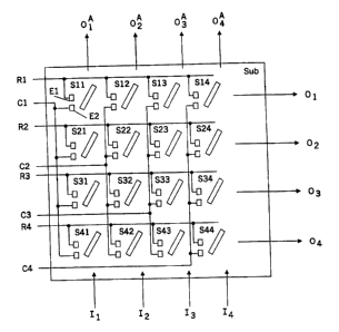
Figure 1 is a schematic drawing of optical cross-connect switches according to
embodiments of the present invention.
Figures 2A and 2B are perspective views of optical cross-connect switches
according
to embodiments of the invention illustrating a positional relationship between
a non-reflective
state and a reflective state.
Figure 3A is a top view of pop-up mirrors according to embodiments of the
present
invention.
Figure 3B is a top view of other pop-up mirrors according to embodiments of
the
present invention.
Figure 4 is a cross-sectional view taken along the line 4-4' of Figure 3B.
9
CA 02363612 2001-11-20
Doc. No: CRO-51 CA Patent
Figure 5 is a cross-sectional view taken along the line 5-5' of Figure 3B.
Figure 6 is an electrical schematic diagram of 4x4 optical cross-connect
switches
according to embodiments of the present invention.
Figure 7 is a flowchart illustrating operations for configuring n x n optical
cross-
connect switches according to embodiments of the present invention.
Figures 8-13 are schematic representations of optical cross-connect switches
according
to embodiments of the present invention during various operational phases of
Figure 7.
Figure 14 is a cross-sectional view taken along the line 14-14' of Figure 3A.
Figure 15 is a flowchart illustrating other operations for configuring n x n
optical
cross-connect switches according to embodiments of the present invention.
Figures 16-20 are schematic representations of optical cross-connect switches
according to embodiments of the present invention during various operational
phases of
Figure 15.
Figure 21 is an electrical schematic diagram of other optical cross-connect
switches
according to embodiments of the present invention in which electronic switches
also are used.
Detailed Description of Preferred Embodiments
The present invention now will be described more fully hereinafter with
reference to
the accompanying drawings, in which preferred embodiments of the invention are
shown.
This invention may, however, be embodied in many different forms and should
not be
construed as limited to the embodiments set forth herein. Rather, these
embodiments are
provided so that this disclosure will be thorough and complete, and will fully
convey the
scope of the invention to those skilled in the art. In the drawings, the
thickness of layers and
regions are exaggerated for clarity. Like numbers refer to like elements
throughout. It will be
understood that when an element such as a reflector is referred to as being
"on" another
element, it can be directly on the other element or intervening elements may
also be present.
In contrast, when an element is referred to as being "directly on" another
element, there are no
intervening elements present. Also, when an element is referred to as being
"connected" or
"coupled" to another element, it can be directly connected or coupled to the
other element or
intervening elements may be present. In contrast, when an element is referred
to as being
CA 02363612 2001-11-20
Doc. No: CRO-51 CA Patent
"directly connected" or "directly coupled" to another element, there are no
intervening
elements present.
As used herein, the term "optical radiation" can include radiation that can be
used to
transmit data in a communications system, such as radiation in the visible,
ultraviolet, infrared
and/or other portions of the electromagnetic radiation spectrum. Although the
present
invention is described herein by reference to MEMS actuators, it will be
understood that the
present invention may be utilized with other actuators. As used herein, the
term optical
"switch" can include optical devices that function as multiplexers,
demultiplexers, and
switches.
Referring now to Figure 1, a schematic drawing of optical cross-connect
switches
according to embodiments of the present invention is shown. As shown in Figure
1, these
embodiments of optical cross-connect switches are formed on a substrate SUB
which
preferably is a microelectronic substrate such as a silicon semiconductor
substrate. However,
many other substrates may be used. A plurality, here four, of input optical
paths h-I4, and a
plurality, here four, of output optical paths Ol-04 are provided. The input
and output optical
paths I and O may be free space and/or fiber optical paths. A plurality, here
four, of
passthrough optical output paths O; -04 also are provided, which pass through
the optical
signals on the input optical paths h-I4 in the absence of switching. As shown
in Figure 1, the
substrate SUB includes four edges with the input optical paths and output
optical paths on
adjacent edges, and the passthrough optical output paths OA on an edge
opposite the input
optical paths.
An array, here sixteen, of microelectromechanical optical switches S11-S44
also are
provided on the substrate, and are arranged in a plurality, here four, of
rows, and a plurality,
here four, of columns. It will be understood that the rows need not be
horizontal and the
columns need not be vertical. Rather, the terms "row" and "column" are merely
used to
indicate any two different directions on the substrate.
The electromechanical optical switches S are responsive to an electromagnetic
(electrical and/or optical) signal to selectively couple the plurality of
input optical paths I to
the plurality of output optical paths O. The electromechanical optical
switches preferably
include reflectors such as mirrors. It will be understood by those having
skill in the art that
the movement may be a rotation about an axis that lies in the plane of the
substrate, rotation
11
CA 02363612 2001-11-20
Doc. No: CRO-51 CA Patent
about an axis that lies orthogonal to the substrate, translation along the
substrate in any
direction, movement into the substrate, movement away from the substrate
and/or any other
movement, as is well known to those having skill in the art. The
electromechanical optical
switches preferably include a reflector on one or more surfaces thereof, to
selectively reflect
an optical signal from an input optical path to an output optical path. The
design of optical
cross-connect switches as described in this paragraph is well known to those
having skill in
the art, and need not be described further herein.
Still refernng to Figure 1, these embodiments of optical cross-connect
switches further
include a plurality, here four, of row address lines Rl-R4, a respective one
of which is
electromagnetically (electrically and/or optically) coupled to a respective
row of the
electromechanical optical switches. A plurality, here four, of column address
lines C1-C4
also is included, a respective one of which is electromagnetically coupled to
a respective
column of the electromechanical optical switches. Preferably, the row address
lines R1-R4
and the column address lines C1-C4 form input/output lines on a fourth edge of
the substrate,
opposite the output optical paths O1-04.
As will be described in detail below, in some embodiments the
electromechanical
optical switches S are configured to be selected upon selection of the
respective row address
line R and column address line C, but not to be selected upon selection of
neither or only one
of the respective row address line and column address line. In other
embodiments, the
electromechanical optical switches S are configured to be selected except for
an
electromechanical optical switch that is electromagnetically coupled to the
selected row
address line and column address line. The selected electromechanical optical
switch or
switches may remain stationary, or may move, depending upon the configuration
of the
optical cross-connect switch.
As shown in Figure 1, by providing a plurality of row address lines and a
plurality of
column address lines, the number of control lines can be less than the number
of switches, and
preferably equal or proportional to the sum of the number of rows and the
number of columns.
Thus, in the embodiments of Figure l, four rows and four columns of switches
S11-544 are
provided, for a total of sixteen switches. Conventional optical cross-connect
switches
generally use sixteen control lines to individually select a switch. In
contrast, embodiments of
Figure 1 can use four row address lines and four column address lines, for a
total of eight
12
CA 02363612 2001-11-20
Doc. No: CRO-51 CA Patent
control lines, which is equal to the sum of the number of rows and the number
of columns, or
less than the sum of the number of rows and the number of columns plus one. A
reduced
number of control lines thereby may be provided. Moreover, the reduction of
control lines
can continue as the number of input optical paths and/or output optical paths
increases,
because the row and column address lines can increase in proportion to the
number of rows
and number of columns whereas, conventionally, the number of control lines
increases in
proportion to the total number of switches. Thus, for an n x n array of
switches, 2n+2 control
lines rather than n2+ 2 control lines may be used, taking into account the
control lines for the
top and bottom electrodes that are described below.
Still referring to Figure 1, each of the electromechanical optical switches
S11-S44
includes a first electrode El and a second electrode E2. A respective first
electrode E1 is
electromagnetically coupled to a respective row address line R and a
respective second
electrode E2 is electromagnetically coupled to a respective column address
line C. In some
embodiments that will be described in detail below, the electromechanical
optical switches S
are configured such that activation of both the first and second electrodes E1
and E2 by the
respective row and column address lines R and C, respectively, allows movement
of the
respective electromechanical optical switch, but activation of neither or only
one of the first
and second electrodes E1 and E2, respectively, prevents movement of the
respective
electromechanical optical switch. In other embodiments, the electromechanical
optical
switches S11-S44 are configured such that activation of both the first and
second electrodes
E1 and E2 by the respective row and column address lines R and C prevents
movement of the
respective electromechanical optical switch, but activation of neither or only
one of the first
and second electrodes E1 and E2 allows movement of the respective
electromechanical
optical switch.
In yet other embodiments that will be described below, the first and second
electrodes
may be attached to, and move with, the reflector. In yet other embodiments,
the first
electrodes are attached to, and move with, the reflector and the second
electrodes are detached
from and do not move with the reflector. Alternatively, the second electrodes
may be
attached to, and move with, the reflector, and the first electrodes may be
detached from, and
do not move with, the reflectors. The first and second electrodes can clamp
the reflector in
13
CA 02363612 2001-11-20
Doc. No: CRO-51 CA Patent
the first position or in the second position when both the first and second
electrodes are
activated, and can allow the reflector to move otherwise.
In still other embodiments that will be described in detail below, each of the
electromechanical optical switches S11-S44 includes an electronic switch that
is electrically
coupled to the respective row and column line. The electronic switch may be a
transistor such
as a field effect transistor.
Other embodiments of the present invention can provide electromechanical
switch
systems that include a plurality of inputs that are not optical inputs and a
plurality of outputs
that are not optical outputs. An array of electromechanical switches are
arranged in the
plurality of rows and a plurality of columns, and selectively moved to couple
the plurality of
inputs to the plurality of outputs. A plurality of row address lines and a
plurality of column
address lines also are provided. The plurality of inputs, the plurality of
outputs, the array of
electromechanical switches, the plurality of row address lines and the
plurality of column
address lines are provided on a common substrate, such as a microelectronic
substrate.
Accordingly, electromechanical switching arrays may be provided that switch,
for example,
electrical input signals, and can include a reduced number of control lines
due to the row and
column addressing. The reduced number of control lines compared to an
individual control
line for each switch can allow these electromechanical switch systems to be
fabricated on a
common microelectronic substrate.
Figures 2A and 2B are perspective views of MEMS electromechanical optical
switches according to embodiments of the invention, illustrating a positional
relationship
between a non-reflective state of an electromechanical optical switch and a
reflective state of
the electromechanical optical switch. A switch 210 includes a first substrate
212, such as a
microelectronic substrate, having a generally planar surface. The first
substrate may comprise
silicon, although other suitable semiconductor or non-semiconductor materials
may also be
used. The electromechanical optical switches of these embodiments include
mirror
assemblies 214 that rotate from parallel to the substrate 212 to orthogonal to
the substrate 212.
These mirror assemblies also are referred to herein as "pop-up mirrors" 214.
Thus, as shown
in Figure 2A, a pop-up mirror 214 is disposed on the surface of the first
substrate 212. In
Figure 2A, the pop-up mirror is positioned in a plane that lies generally
parallel to the surface
of the first substrate. In this pop-up mirror orientation, referred to herein
as the non-reflective
14
CA 02363612 2001-11-20
Doc. No: CRO-51 CA Patent
state, optical signals may pass by the mirror without being altered or
reflected. In contrast, in
Figure 2B, the pop-up mirror 214 is positioned in the plane that lies
generally perpendicular to
the surface of the first substrate 212. In this pop-up mirror orientation,
referred to herein as
the reflective state, an input optical signal, represented in Figure 2B by
arrow 216a will
contact the reflective surface 218 of the pop-up mirror 214 and change the
optical path to
produce an output optical signal 216b.
The optical cross-connect switch may also comprise a second substrate, such as
a
second microelectronic substrate, that is disposed in a fixed positional
relationship relative to
the first substrate, preferably spaced apart from and facing the first
substrate. The second
substrate is not shown in the simplified perspective views of Figures 2A and
2B, but will be
described in detail below. One or more positioning structures may be disposed
relative to the
first substrate 212 and the pop-up mirror 214, to impede further movement of
the pop-up
mirror beyond the desired reflective state. They also may include clamping
electrodes that
clamp the mirror 214 in the reflective state, as will be described in detail
below. In the
embodiments shown in Figures 2A and 2B, the positioning structures 222 are
pillar-like
structures extending from the second substrate toward the planar surface of
the first substrate
212. The positioning structures 222 may approach but not contact the first
substrate 212, to
provide electrical isolation between the first and second substrates. In other
embodiments,
they may contact the second substrate. In still other embodiments, an
insulating layer may be
provided either on the first substrate 212 or on the end portion of the
positioning structures
that will allow the positioning structures to come into contact with the first
substrate 212 and
still maintain electrical isolation.
As shown in Figure 2B, the pop-up mirror 214 is restricted from further
movement by
the two positioning structures 222. Moreover, tabs 225a and 225b that are
coupled to the
?5 sides of the pop-up mirror 214 and can contact each positioning structure
222, to restrict the
movement of the pop-up mirror 214. It is also possible to configure the
positioning structures
so that the pop-up mirror contacts and is restricted by only one positioning
structure. In some
embodiments of the present invention, the tabs 225a and 225b are electrically
isolated from
one another, to form first and second movable electrodes for the pop-up mirror
214 that move
with the pop-up mirror. In other embodiments, the tabs 225a and 225b are
electrically
connected to one another to form a single movable electrode for the pop-up
mirror. It also
CA 02363612 2001-11-20
Doc. No: CRO-51 CA Patent
will be understood that the reflective surface 218 may be positioned on the
opposite side of
the pop-up mirror 212 from that shown in Figures 2A and 2B.
Embodiments of pop-up mirrors are shown in more detail in the top view of
Figure
3A. The pop-up mirror 314 is disposed on a generally planar surface of a first
substrate 312.
A sacrificial layering process may be employed during the fabrication of the
pop-up mirror to
allow for the mirror to be released from the surface of the first substrate
312 and overlie a
trench 330 in the first substrate. The trench 330 can provide electrical
isolation between the
pop-up mirror 314 and the substrate and also can reduce problems related to
the pop-up mirror
sticking to the substrate (commonly referred to as "suction" force by those of
ordinary skill in
the art) during fabrication and during device use. In lieu of fabricating a
trench, it also may
be possible to texture the underside of the pop-up mirror, the substrate or
both surfaces with a
dimple-like array pattern. The dimpled surface may provide less contact
surface area between
the mirror and substrate, thus, lessening the problems encountered with
stiction.
Still referring to Figure 3A, tabs 325 can restrict further movement of the
pop-up
mirror 314 upon actuation and rest upon the substrate 312 in the non-actuated
position and
serve to support the pop-up mirror 314 above the trench 330. The tabs 325 may
be
electrically conductive to provide a movable electrode that moves with the pop-
up mirror 314,
so that a voltage that is applied to the tabs may serve to clamp the pop-up
mirror in an
actuated reflective position or in a non-actuated, non-reflective position.
A tether device 332 is used to impart mobility to the pop-up mirror and
provide an
electrical path for transmitting electrostatic voltage to the tabs 325 of the
pop-up mirror. As
shown in the embodiments of Figure 3A, the tether device 332 may comprise an
elongated
oval shaped tether, commonly referred to as a hairpin tether. This
configuration of the tether
332 can provide a robust and flexible structure. The use of tether devices and
more
specifically, hairpin tethers is shown by way of example. Other tether
configurations and
flexible hinge type mechanisms also may be used to impart the desired mobility
to the
attached pop-up mirror 314. For clarity sake only, Figures 2A and 2B did not
illustrate a
tether device or hinge type mechanism.
The tether device 332 is attached to the substrate at an anchor 334. The
tether device
332 can impart a force to hold the pop-up mirror in the stationary non-
reflective state (i.e.
generally parallel to the substrate 312). In these embodiments, the hairpin
tether also can
16
CA 02363612 2001-11-20
Doc. No: CRO-51 CA Patent
provide a bending and/or twisting of the oval-shaped tether to restore the pop-
up mirror 314
from the reflecting state to the non-reflecting state.
The tether device 332, the anchor 334, the tabs 325 and an underlying base
plate of the
pop-up mirror (not shown in Figure 3A) may comprise the same material, such as
polysilicon.
It is also possible to form the tether device, the anchor, the tabs and/or the
underlying base
plate from other flexible, electrically conductive materials. If the anchor,
the tether device,
the tabs and the underlying base plate of the pop-up mirror comprise one
material, such as
polysilicon, it is possible to form the structures during a single fabrication
process. The
reflective surface 318 of the pop-up mirror 314 may comprise gold or other
suitable reflective
materials. In Figures 3A and 3B, the reflective surface 318 is on the bottom
surface of the
pop-up mirror 314. However, the reflective surface also may be on the top
surface as shown
in Figures 2A and 2B. The frame 326 that surrounds the reflective surface may
comprise
electroplated nickel. The frame 326 of the pop-up mirror 314 can provide
rigidity to the
overall pop-up mirror and, in some embodiments, can provide a magnetically
active material.
Other materials that provide similar characteristics may also be used to form
the frame
structure. In some embodiments, the frame 326 and the reflective surface 318
may be on the
same face of the pop-up mirror 314. In other embodiments, the frame 326 may be
on the
opposite face as reflective surface 318. When the frame is on the opposite
face, nickel plating
may be used on a portion or all of the surface. When on the entire opposite
face, the nickel
plating still may be regarded a frame, because it includes a supporting and/or
magnetically
active layer.
Still referring to Figure 3A, according to embodiments of the present
invention, a
respective column address line C is electromagnetically, here electrically,
coupled to the tab
325 via the tether device 332. Thus, the tab 325 can provide a movable first
electrode. The
coupling of column line C to the tether device 332 may take place at a
coupling point 336, at
the anchor 334 and/or at other points. Thus, the tab 325 forms a movable
column electrode,
also referred to herein as a column flap electrode 325. As also shown in
Figure 3A, a row
address line R is electromagnetically, here electrically, coupled to a
stationary electrode 338'
on the substrate 312. Thus, the electrode 338' can provide a stationary second
electrode. It
will be understood that in other embodiments, the tab 325 may be electrically
coupled to the
row address line and the substrate electrode 338' may be coupled to the column
address line.
17
CA 02363612 2001-11-20
Doc. No: CRO-51 CA Patent
Figure 3B describes alternate embodiments of pop-up mirrors 314' according to
other
embodiments of the present invention. In Figure 3B, two portions 332a and
332b, here
halves, of the hairpin tether device are electrically isolated from one
another by an insulating
layer 333 and tab electrode portions also are electrically isolated from one
another using the
same insulating layer 333 and/or a different insulating layer, to provide
electrically isolated
tabs 325a and 325b. The right hand tab 325a is electrically connected to the
row address line
R via the right half of the frame 326a, the right half of the tether 332a, at
a coupling point
336a, to thereby provide a row flap electrode 325a that moves with the pop-up
mirror 314'.
Similarly, the left tab 325b is electrically connected to the column address
line C via the left
half of the frame 326b and the left half of the tether device 332b, to provide
a column flap
electrode 325b that moves with the pop-up mirror 314'. Operation of optical
cross-connect
switches using embodiments of Figures 3A and 3B according to embodiments of
the present
invention will be further described in detail below.
In contrast, in conventional magnetically actuated OXC devices using
electrostatic
clamping, the substrate may be used as a single global electrode and the
mirror flaps may be
used as an addressable electrode that forms the second electrode of the
capacitor between the
mirror flap and the substrate, to provide electrostatic clamping. Thus,
conventionally, a
separate control line may be used for each mirror in the array, to
individually address each
mirror. Thus, for an n x n array of mirrors, n2 control lines may be needed.
In some embodiments of the invention a pop-up mirror is actuated by the use of
a
magnetic field that extends generally orthogonal to the first and second
substrates. As a
magnetic field is applied that is generally orthogonal to the first and second
substrates, a
magnetically active pop-up mirror will attempt to align itself with the
direction of the field.
An electrostatic field may be applied to the pop-up mirror to hold the mirror
in a stationary
non-reflective position (i.e. parallel to the first substrate). If a magnetic
field is employed, the
electrostatic field should be of such strength that it overrides the magnetic
field. Once the
electrostatic field is removed, the magnetic field can become dominant and
provide force to
actuate the pop-up mirror. In embodiments using magnetic field actuation, the
frame and/or
other layer may serve as the magnetically active component of the pop-up
mirror. The
magnetic field that may be used may comprise external permanent magnets,
electromagnets
and/or any other magnets capable of generating the requisite magnetic field.
18
CA 02363612 2001-11-20
Doc. No: CRO-51 CA Patent
In some embodiments of the invention the optical cross connect switch may
employ an
external magnetic field that generates a magnetic field generally
perpendicular to the planar
surface of the first substrate. Such a magnetic field may be generated by the
use of a
permanent magnet or electromagnets. The magnetic field typically may be on the
order of
200-500 gauss. An electromagnet may be located below the surface of the first
substrate and
serves to generate a magnetic field generally perpendicular to the first and
second substrates.
The magnetic field can cause the magnetic component of the pop-up mirror to
align with the
axis of the magnetic field, creating torque acting against the torsion of the
tether. The use of
an electromagnet is described by way of example. Other magnetic field
generators, such as
permanent magnets, also may be used to generate the magnetic field.
Figure 4 is a cross-sectional view of Figure 3B, taken along the line 4-4' of
Figure 3B,
and may be regarded as a "unit cell" of embodiments of electromechanical
optical switches
according to embodiments of the present invention. The row flap electrode 325a
also will
referred to as a row clamp electrode 325a and the column flap electrode 325b
also will be
referred to as a column clamp electrode 325b. The row clamp electrodes 325a in
a row of the
array are all connected in common and the column clamp electrodes 325b in a
column of the
array are all connected in common. The stationary electrode 338 on the
substrate 312 also
will be referred to herein as a bottom or lower clamp electrode 338.
Figure 5 is a cross-sectional view taken along the line 5-5' of Figure 3B, and
illustrates
a "bed-of-nails" second substrate 510, which includes an upper clamp electrode
512 in and/or
on the nails or protrusions thereof. It will be understood that the upper
clamp electrode 512
may be defined using a conductive layer on the nail and/or by providing a
conductive or
partially conductive nail using techniques well-known to those having skill in
the art and as
described in detail in the above-cited Application Serial No. 09/489,264. It
also will be
understood that Figure 5 is a simplified cross-sectional view, wherein only
features of the
devices that are relevant to the clamping of mirrors are shown. The pole
pieces,
electromagnet and external magnet circuit are not shown for clarity. However,
embodiments
of these elements are illustrated in the aforesaid Application Serial No.
09/489,264.
Embodiments of Figures 3B, 4 and 5 may be used in an m x n array or an n x n
array,
with the column clamp electrodes 325b of each mirror 314' in a column of the
array
electrically coupled together as a column control line C. The column control
line may be
19
CA 02363612 2001-11-20
Doc. No: CRO-51 CA Patent
brought off the substrate 312 for external control. Similarly, the row clamp
electrodes 325a
of each row of mirrors in the array are electrically connected as the row
control lines R and
may be brought off the substrate 312 for external control. Thus, for an n x n
array of mirrors,
2n control lines may be used. This can result in fewer control lines and
signals for n > 2, and
can result in less area for routing and wire bonding on an n x n OXC
substrate.
All of the upper clamp electrodes 512 may be coupled together electrically on
the bed-
of-nails substrate 510 so that only a single electrical connection may be
used. Similarly, the
lower clamp electrodes 338 all may be coupled together electrically so that a
single electrical
connection may be used.
Figure 6 is an electrical schematic diagram of embodiments of a 4 x 4 array of
Figures
3B, 4 and 5, including parasitic bus capacitances Cb"S that generally will be
present between
signal lines and the substrate. Operations for configuring embodiments of an n
x n OXC
and/or individual mirror operations for strictly non-blocking n x n OXC
switches will be
described in connection with the flowchart of Figure 7, and are illustrated
conceptually in
Figures 8-13.
It will be understood that the operations of the flowchart of Figure 7 and
Figures 8-13
may be performed by a controller that is located on the same substrate 312 as
the optical
cross-connect switch and/or external to the substrate 312 ("off-chip"). The
overall design of
controllers for optical cross-connect switches are well known to those having
skill in the art
and need not be described further herein. Moreover, although operations now
will be
described using voltages +V and OV, other voltages may be used. Finally,
although the
bottom clamp electrode 338 and top clamp electrode 512 are shown as being
maintained at the
same voltage +V, they may be maintained at different voltages, as long as
potential
differences with the row and column flap electrodes 325a and 325b are
maintained as
described below. It also will be understood that in all of Figures 3A-21, the
optical paths are
not shown for the sake of clarity.
Referring now to Figure 7, at Block 710, in the quiescent state, each pop-up
mirror
314' remains clamped to either the top clamp electrode 512 or the bottom clamp
electrode
338. As shown in the embodiments of Figure 8, the top and bottom clamp
electrodes 512 and
338 are maintained at +V, for example by connecting these electrodes to a
power supply
voltage +V. All the row and column lines Rl-R4 and C1-C4 are connected to
ground (0V).
CA 02363612 2001-11-20
Doc. No: CRO-51 CA Patent
No global magnetic field B is applied. In this state, a voltage V is present
across all the down
and up mirror electrostatic clamp capacitors that are formed between the row
and column
clamp electrodes 325a and 325b and/or the frame sections 326a and 326b, and
either the
bottom clamp electrode 338 or the top clamp electrode 512.
It will be understood that the voltage V preferably is selected to be
sufficient to ensure
clamping of the mirror in both up and down states of the mirror, even in the
presence of the
global magnetic field B that is used for actuation to flip mirrors up.
Moreover, the potential V
preferably is chosen to be sufficient to ensure clamping of the mirror in both
the up and down
states of the mirror, even when the potential V appears only across only one
of the row flap
electrode 325a or the column flap electrode 325b. Thus, in Figure 8, all of
the mirrors 314'
remain in their existing configuration. Thus, switches S13, S24, S32 and S41
are clamped in
the up position to switch the input optical path to the output optical paths,
whereas the
remaining switches remain clamped in their down position, so as not to block
an input optical
path.
Referring now to Block 720 of Figure 7 and to Figure 9, the global magnetic
field B is
turned off or remains off and all the row and column control lines Rl-R4 and
C1-C4 are
connected to the power supply voltage +V, to unclamp all the mirrors in the up
state and bring
them down, as indicated by the arrows 910 in Figure 9. The torque imparted by
the tether 332
can restore the mirrors to the non-reflective state.
Then, at Block 730 of Figure 7 and in Figure 10, all of the row and column
lines R1-R4 and
C1-C4 are connected to OV, thereby clamping all of the mirrors 314' to the
bottom electrode.
Then, as shown in Block 740 of Figure 7 and in Figure 11, a selected row and
column
electrode is brought to +V, and the global magnetic actuation B field is
applied. In the
example of Figure 11, row R2 and column C2 are both connected to +V, and the
global
magnetic field B is turned on. This unclamps the switch S22 in the selected
position, since
both the row and column flap electrodes 325a and 325b for this switch S22 have
zero
potential drop with respect to the bottom clamp electrode 338. Thus, the
switch S22 will start
to move up in the presence of the global magnetic field B. It will be
understood that the
remaining switches S21, S23 and S24 in the second row that have their row flap
electrodes
325a connected to +V, but their column flap electrodes 325b at OV will not be
flipped
because the potential drop V still is present. Similarly, the remaining
switches in the second
21
CA 02363612 2001-11-20
Doc. No: CRO-51 CA Patent
column that have only one electrode at +V, i.e. switches S12, S32 and S42,
also will not flip.
Finally, the remaining switches that have both their row flap electrodes 325a
and column flap
electrodes 325b at OV also will not flip.
Referring now to Block 750 of Figure 7 and to Figure 12, after a predetermined
time at
which the moving mirror is out of the "recapture" zone of the bottom electrode
338, the
selected row and column lines again may be connected to OV. This resetting is
performed so
that the flipped mirror can clamp to the top clamp electrode 512, as shown in
Figure 12.
Then, referring to Block 760 of Figure 7, a determination is made if
additional
switches are to be flipped. If yes, the operations of Block 740 and 750
corresponding to
Figures 11-12 are again performed. If not, operations return to the quiescent
state of Block
710 and Figure 8.
Figure 13 illustrates a final configuration, wherein four switches 511, 522,
S23 and
S44 are flipped, to thereby switch input h to output Ol, input I2 to output
O2, input I~ to
output 03 and input I4 to output 04. Thus, the OXC has been reconfigured.
It will be understood by those having skill in the art that the above-
described
embodiments of Figures 3B-13 have been described in the context of
magnetically global
actuated optical cross-connect switches, but can be extended for
nonmagnetically actuated
optical cross-connect switches and also may be extended to any array of other
switching
devices that can use global actuation and electrostatic clamping to clamp the
device in initial
and final states, and/or other electromechanical switching arrays. In the
embodiments of
Figures 3B-13, the clamping electrode is separated into two portions, one a
row portion and
the other a column portion.
Other embodiments of the invention now will be described. In particular, as
was
described in connection with Figure 3A, these embodiments of optical switches
do not
employ a split flap electrode. Rather, each flap electrode 325 is electrically
connected to an
appropriate column address line C. The lower or bottom clamp electrodes 338'
are not all
connected in common, but rather are connected to an appropriate row address
line R. Thus, in
contrast with Figure 3B, the lower electrode 338' is patterned so that all of
the lower
electrodes 338' in a row are connected to a row address line R.
Figure 14 is a cross-sectional view taken along the line 14-14' of Figure 3A.
In Figure
14, an individual lower electrode 338' is provided below each flap electrode
325. The lower
22
CA 02363612 2001-11-20
Doc. No: CRO-51 CA Patent
electrode 338' can be fabricated by implanting dopant into the face of the
substrate 312
- through a mask, by depositing an additional conductive layer such as
polysilicon and/or by
using other conventional techniques. The left and right portions of the lower
electrode 338'
for each individual switch are electrically connected together, as are the two
portions of the
flap electrode 325. The flap electrodes 325 of each switch in a column of the
array are
electrically coupled together as a column address signal C. The column address
signals may
be brought off-chip. Similarly, the bottom electrodes 338' of each row of
switches in the
array are electrically connected as row address lines R and may be brought off-
chip. Thus,
for an n x n array of switches 2n+2 control lines may be used.
Figure 15 is a flowchart illustrating operations for configuring an array of
switches
according to embodiments of Figures 3A and 14. Rather than describe the array
of switches
in a schematic top view, as was the case for Figures 8-13, the operations of
Figure 15 will be
described using electrical schematic diagrams of Figures 16-20, including the
capacitances of
the switches.
Referring now to Figure 15, in the quiescent state as shown at Block 1510,
each of the
switches remains clamped to the top electrode 512 or the bottom electrode
338'. This is
illustrated in the electrical schematic diagram of Figure 16. As shown in
Figure 16, all of the
row address lines Rl-R4, corresponding to the patterned bottom electrodes
338', are
maintained at a first voltage such as -V, and all of the column electrodes C1-
C4,
corresponding to the column flap electrodes 325 are maintained at OV. The top
electrode 512
also is maintained at -V. Thus, since the flap electrodes are maintained at OV
and the top
electrode 512 and the bottom electrodes 338' are maintained at -V, clamping to
the top or
bottom electrodes will take place. In this state, a voltage V is present
across all the down and
up switches. The potential V is selected to be sufficient for clamping in both
up and down
states of the mirror, even in the presence of the global magnetic field B that
is used for
actuation to flip mirrors up. During the quiescent state, however, the global
magnetic field
preferably is not applied.
As shown in Figure 16, switches 513, 524, S32 and S41 are clamped up, with the
voltage of the top electrode 512 being indicated by V~. The remaining switches
are clamped
down with the voltage -V appearing between the bottom electrode 338' and the
flap electrode
325. The bus capacitance Cb"s also is shown.
23
CA 02363612 2001-11-20
Doc. No: CRO-51 CA Patent
Referring now to Block 1520 of Figure 15 and to Figure 17, the switches are
all
returned to their unclamped state to move all of the switches down. In
particular, as shown in
Figure 17, all the column control lines are connected to -V, to unlatch all
the switches in the
current up state and rotate them down, due to the restoring force of the
tether 332. Thus, as
shown in Figure 17, all of the flaps are shown as down, and are clamped to the
bottom
electrode 338.
Referring now to Block 1530 of Figure 15 and to Figure 18, a potential +V is
applied
to the column and row select lines of the switch positions to be flipped up.
For example, as
shown in Figure 18, the potential of row R2 and column C2 is changed from -V
to +V. All
the other column select lines are maintained at OV, and all the other row
lines are maintained
at -V. This clamps all the switches except the switch S22 in the selected row
and column.
The global magnetic field B then is applied, for example by providing current
to an
electromagnet. This will cause the unclamped switch, switch S22 in Figure 13,
to begin
flipping up.
Then, referring to Block 1540 of Figure 15 and to Figure 19, after a
predetermined
time at which the moving switch is out of the "recapture" zone of the bottom
electrode 338',
the selected column and row address lines, here C2 and R2, are set back to
their steady state
levels of OV and -V, respectively.
Referring now to Block 1550 of Figure 15, if additional switches are to be
selected,
then the operations of Blocks 1530 and 1540, corresponding to Figures 18 and
19, are again
repeated. A final configuration is shown in Figure 20, in which switches 511,
522, S33 and
S44 have been flipped. Global actuation then may be turned off and the
quiescent state is
obtained.
Figure 21 is an electrical schematic diagram of other embodiments of the
present
invention, in which an electronic switch 2110 is electrically coupled to the
respective row and
column lines. The electronic switch may include one or more bipolar
transistors, field effect
transistors and/or other electronic switching devices. In embodiments of
Figure 21, a field
effect transistor is shown, including a controlling electrode (gate) 2110c and
a pair of
controlled electrodes (source or drain) 2110a and 2110b. The controlling
electrode 2110c is
connected to the corresponding row address line R1-R4 and one of the
controlled electrodes
2110a is connected to the corresponding column line C1-C4. The other
controlling electrode
24
CA 02363612 2001-11-20
Doc. No: CRO-51 CA Patent
2110b is connected to the lower clamp electrode 338'. All of the flap
electrodes 325 are
connected to ground.
It will be understood that embodiments of Figure 21 may need to use more
complex
fabrication processes in order to fabricate transistors on the same
microelectronic substrate as
the electromechanical switches 312. Moreover, a dynamic charge storage scheme
similar to
refreshing of a Dynamic Random Access Memory (DRAM) that includes a transistor
and a
capacitor, also may need to be provided during the time the optical cross-
connect switches are
reconfigured. Unlike a conventional DRAM, charge refresh may not be needed in
the
quiescent state.
In order to configure embodiments of optical cross-connect switches of Figure
21, all
the switches are reset, for example by applying OV to all of the row lines R
and/or all of the
column lines C, to turn off the transistors 2110. The column lines C1-C4 then
all are
precharged or set to the voltage +V or OV based upon whether the column
includes the switch
to be flipped. The row select then is enabled to charge all the clamp
capacitors Cmd in the
selected row to the desired voltage. These operations then are performed on
the next row.
After all the clamp capacitors Cmd in the array have the desired voltage, the
global magnetic
field B may be applied to flip the unclamped mirrors up and clamp them in the
up position.
The magnetic field then may be removed. These operations may be analogized to
writing
operations of a one-transistor DRAM, and need not be described further herein.
It will be understood by those having skill in the art that although the above-
described
embodiments have been described in terms of orthogonal rows and columns, the
rows and
columns need not be orthogonal to one another. Rather, the terms "row" and
"column" have
been used arbitrarily to indicate two different directions in a Cartesian,
radial and/or other
coordinate system. Moreover, voltages other than those which were described
may be used,
and different configuration sequences also may be used. Moreover, although the
optical paths
have been omitted from Figures 3A-21, it will be understood that the input
optical paths h-Ia
and the output optical paths O1-04 of Figure 1 may be present in all
embodiments of OXCs of
Figures 3A-21. Although the embodiments have been described in terms of 4 x 4
arrays, any
arbitrary number of rows and columns may be used. Other row and column
addressing
schemes also may be used.
CA 02363612 2001-11-20
Doc. No: CRO-51 CA Patent
Although the switches have been exemplified as mirrors that flip about an axis
of
rotation that is in the plane of the substrate, other actuation techniques may
be used.
Embodiments of the present invention also may be applied to other
electromechanical switch
systems such as relay switch systems that switch electrical signals in
response to an
electromagnetic input, rather than optical switches that switch optical
signals. Finally,
although the switches have been illustrated as being on a single substrate,
multiple substrates
also may be used, and multiple substrates may be coupled to one another to
create larger
devices.
In the drawings and specification, there have been disclosed typical preferred
embodiments of the invention and, although specific terms are employed, they
are used in a
generic and descriptive sense only and not for purposes of limitation, the
scope of the
invention being set forth in the following claims.
26