Note: Descriptions are shown in the official language in which they were submitted.
CA 02363625 2001-11-20
Doc. No. 10-451 CA(2) Patent
OPTICAL SWITCH
Microfiche Aupendix
[0001] Not Applicable
Field of the Invention
[0002] The present invention relates to the field of optical switches.
Background of the Invention
[0003] Optical matrix switches are commonly used in communications systems for
transmitting
voice, video and data signals. Generally, optical matrix switches include
multiple input and/or
output ports and have the ability to connect, for purposes of signal transfer,
any input port/output
port combination, and preferably, for N x M switching applications, to allow
for multiple
connections at one time. At each port, optical signals are transmitted and/or
received via an end
of an optical waveguide. The waveguide ends of the input and output ports are
optically
connected across a switch interface. In this regard, for example, the input
and output waveguide
ends can be physically located on opposite sides of a switch interface for
direct or folded optical
pathway communication therebetween, in side-by-side matrices on the same
physical side of a
switch interface facing a mirror, or they can be interspersed in a single
matrix arrangement
facing a mirror.
[0004] Establishing a connection between a given input port and a given output
port, involves
configuring an optical pathway across the switch interface between the input
ports and the output
ports.
[0005] One way of configuring the optical path between an input port and an
output port
involves the use of one or more moveable mirrors interposed between the input
and output ports.
In this case, the waveguide ends remain stationary and the mirrors are used
for switching. The
CA 02363625 2001-11-20
Doc. No. 10-451 CA(2) Patent
mirrors can allow for two-dimensional targeting to optically connect any of
the input port fibers
to any of the output port fibers.
[0006] An important consideration in switch design is minimizing switch size
for a given
number of input and output ports that are serviced, i.e., increasing the
packing density of ports
and beam directing units. It has been recognized that greater packing density
can be achieved,
particularly in the case of a movable mirror-based beam directing unit, by
folding the optical
path between the fiber and the movable mirror and/or between the movable
mirror and the switch
interface. Such a compact optical matrix switch is disclosed in U.S. Patent
No. 6,097,860. In
addition, further compactness advantages are achieved therein by positioning
control signal
sources outside of the fiber array and, preferably, at positions within the
folded optical path
selected to reduce the required size of the optics path.
[0007] Current switch design continuously endeavors to accommodate more fibers
in smaller
switches.
[0008] The general approach in the field of optical cross-connects (OXCs) is
to individually
collimate each input fiber, and "throw" the beam to its dedicated mirror.
[0009] It is an object of this invention to provide an optical switch wherein
an input fiber array is
imaged to a mirror.
[0010] It is another object of the invention to image the input fiber array to
a MEMS mirror
array.
[0011] It is a further object of the invention to provide a compact optical
switch or optical cross-
connect.
Summary of the Invention
2
CA 02363625 2001-11-20
Doc. No. 10-451 CA(2) Patent
[0012] In accordance with the invention there is provided, an optical switch
comprising an input
port for launching a beam of light into the optical switch; a plurality of
output ports, each output
port for selectively receiving the beam of light; beam directing elements for
selectively directing
the beam of light from the input port to any one of the plurality of output
ports; and an element
having optical power for imaging the beam of light.
[0013] In accordance with the invention, there is further provided, an optical
switch comprising:
a plurality of input ports for launching a plurality of light beams into the
optical switch; a
plurality of output ports, each output port for selectively receiving any one
of the plurality of
light beams; an optical imaging system for imaging the plurality of light
beams from the plurality
of input ports to an imaging plane and from the imaging plane to the plurality
of output ports;
and beam directing elements for selectively directing the plurality of light
beams from any one of
the plurality of input ports to any one of the plurality of output ports, the
beam directing elements
being disposed between one of the plurality of input ports and output ports
and the imaging
plane.
[0014) In accordance with another aspect of the invention, there is provided,
an optical switch
for being operated in one of transmissive and a reflective mode of operation
comprising: a
plurality of input fibers for launching a plurality of light beams into the
optical switch; a plurality
of output ports for selectively receiving the plurality of light beams from
any one of the plurality
of input ports; an imaging system for one of imaging the light beams from the
plurality of input
fibers to an imaging plane and from the imaging plane to the plurality of
output fibers; and beam
directing means for intercepting the light beams that were launched into the
optical switch before
said light beams are imaged to the imaging plane and for selectively directing
the light beams
from any one of the plurality of input fibers to any one of the plurality of
output fibers.
[0015] In accordance with an embodiment of the present invention, the at least
one input port
and the plurality of output ports are disposed in an object plane of the
imaging system.
Brief Description of the Drawings
3
CA 02363625 2001-11-20
Doc. No. 10-451 CA(2) Patent
[0016] Exemplary embodiments of the invention will now be described in
conjunction with the
drawings in which:
[0017] Fig. 1 shows a prior art optical switch wherein the beam of each input
waveguide is
individually collimated;
[0018] Fig. 2 presents a schematic view of the optical system of a switch in a
reflective
configuration with one imaging lens;
[0019] Fig. 3 shows a schematic view of the imaging function of the imaging
lens;
[0020] Fig. 4 presents a schematic view of the reflective optical system of
the switch using a
telecentric imaging system;
[0021] Fig. 5 shows a close up view of section A of Fig. 4;
[0022] Fig. 6 shows a schematic view of the two-dimensional array of the fiber
bundle having a
honeycomb structure;
[0023] Fig. 7 shows a schematic view of the two-dimensional array of the MEMS
mirrors having
a honeycomb structure;
(0024] Fig. 8 shows a schematic view of an optical switch in accordance with
the invention in a
transmissive configuration;
[0025] Fig. 9 shows a schematic view of an optical switch in accordance with
the invention
using a mirror system as an imaging system; and
[0026] Fig. 10 shows a schematic view of another optical switch in accordance
with the
invention including another mirror system as an imaging system.
4
CA 02363625 2001-11-20
Doc. No. 10-451 CA(2) Patent
Detailed Description of the Invention
[0027] Turning now to Fig. 1 a prior art optical switch or cross-connect
structure 100 is shown,
wherein micro-mirrors 110 on a MEMS chip 112 are used to fold the design. The
folded optical
pathway configuration allows for a compact switch design using the movable
mirror based beam
directing unit. However, the general approach in this type of prior art
optical cross connectors is
to individually collimate each input waveguide and direct the beam to its
dedicated mirror. This
mirror then deflects this beam to any one of the plurality of output mirrors
which then redirects
the beam, i.e. compensates for the angle, to its dedicated output waveguide.
As is seen from Fig.
1, this design requires the use of a lens 114 for each individual input fiber
of input fiber bundle
116 and each individual output fiber of output fiber bundle 118.
[0028] The present invention provides an optical switch or a large scale fiber-
optical cross-
connect switch wherein the light from the grouped input fibers is collected by
a lens, a lens
system, a mirror, or a mirror system, and imaged with a certain magnification
to an imaging
plane. The imaging plane is either a mirror when the system is operated in
reflection, or a plane
of symmetry when the system is operated in transmission. Before reaching that
plane, the
spatially separated beams are intercepted by a (1 or) 2-D micro mirror input
MEMS array, where
each mirror can deviate its dedicated input beam to any mirror on the output
MEMS array. Each
mirror on the output MEMS array compensates for angular tilt and deviates the
beam to its
dedicated output port.
[0029] This design of the optical switch in accordance with the present
invention is based on a
single lens, a lens system, a mirror, or a mirror system for imaging the input
light beams to a
MEMS 2D mirror array. The optical switch is built in a reflective
configuration or, if desired, in
a transmissive configuration.
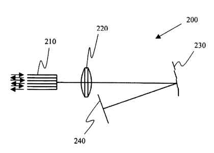
[0030] Fig. 2 presents a schematic view of the optical system of a switch 200
in a reflective
configuration including an input and output fiber bundle 210, an imaging lens
220, a MEMS chip
230 with 2D tiltable micro-mirrors and a bulk mirror 240 disposed in the
imaging plane of the
imaging lens 220. Input fibers of fiber bundle 210 are denoted with an
arrowhead pointing to the
CA 02363625 2001-11-20
Doc. No. 10-451 CA(2) Patent
right and output fibers of fiber bundle 210 are denoted with an arrowhead
pointing to the left of
the figure.
[0031] Fig. 3 shows a schematic view of the imaging function of the imaging
lens 220 from the
input/output fiber bundle 210 to the bulk mirror 240 and not the retro-
reflected beams from the
bulk mirror 240 back to the input/output fiber bundle 210. The geometrical
image of the output
surface of the input/output fiber bundle 210 is slightly behind the mirror
240. As shown, as the
input beams are imaged to the bulk mirror 240, they are intercepted by the
MEMS array 230
once the beams are spatially resolvable. The MEMS array 230 includes input and
output micro
mirrors in this reflective configuration. Each one of the input mirrors on the
MEMS array can
deviate its dedicated input beam angularly and therefore laterally on the bulk
mirror 240, so that
by the time it returns to the MEMS array 230, it has been physically displaced
on the MEMS
chip 230 so that it hits another micro mirror, i.e. one of the output micro
mirrors. This output
micro mirror redirects the beam back through the imaging lens 220 to hit its
dedicated output
port/fiber within the input/output fiber bundle 210.
[0032] There is an optimal relationship between the input and output beam size
and therefore
divergence, and the pitch between the fibers in the array, such that the
distance from the MEMS
chip 230 to the bulk mirror 240 is maximized and such that the number of
connected channels is
maximized.
(0033] While chief rays of each fiber before the lens are parallel to each
other, after passing
through the lens they diverge. Therefore, the micro mirrors should compensate
for non-
telecentricity of beam axes.
(0034] However, if desired, magnification is used to improve the resolvability
of the beams on
the MEMS chip.
(0035] Fig. 4 presents a schematic view of another embodiment of an optical
switch 300 in
accordance with the invention showing a reflective configuration using a
telecentric imaging
system 310. Optical switch 300 further includes an input/output fiber bundle
330 and a bulk
6
CA 02363625 2001-11-20
Doc. No. 10-451 CA(2) Patent
mirror 340. As is seen, the telecentric imaging system 310 keeps the chief
rays of all the input
and output beams parallel to the optical axis when they hit the MEMS chip 320.
Again, if
desired, lateral magnification is used to improve the spatial resolvability of
the beams at the
MEMS chip320.
[0036] Fig. 5 shows a close up view of section A of Fig. 4 of optical switch
300. This close up
view demonstrates more clearly the parallelism of the chief rays of the input
beams of optical
switch 300 at the MEMS chip 320 to the bulk mirror 340.
[0037] It is apparent, that in the reflective configuration the fiber bundle
330 consist of both
input and output fibers, and the MEMS chip 320 consists of an array of
mirrors, each
corresponding to a dedicated input or output fiber. However, it is not
necessary that there be an
equal number of inputs and outputs allowing for the configuration of an NxM
optical cross-
connect.
[0038] In accordance with another embodiment of the present invention, the
structure of the fiber
bundle and the MEMS chip is the same. This is advantageous for improving or
maximizing the
fill-factor. Both, the fiber bundle 610 and the MEMS array 710 can be arranged
in a one-
dimensional array having a linear arrangement or in a two-dimensional array
having a
honeycomb structure, for example. Such a honeycomb structure of a fiber bundle
610 and a
MEMS array 710 is illustrated in conjunction with Figs. 6 and 7.
[0039] In an exemplary embodiment of the invention, optical switch 200 of Fig.
3 has 37 fibers.
These fibers can be a part of 19x 19 switch with one spare fiber, for example.
[0040] If the input and output fibers are distributed uniformly or randomly
over the end face of
the fiber bundle, the size of the bulk mirror 240 should be equal to the size
of the MEMS chip
230. If however, an upper section of the fiber bundle in Fig. 6 is assigned
for input fibers, and a
lower part of the fiber bundle for output fibers, then the size of the bulk
mirror 240 in a vertical
direction can be one half of the size of the MEMS chip. The steering range of
micro mirrors in
this direction can be cut in half as well.
7
CA 02363625 2001-11-20
Doc. No. 10-451 CA(2) Patent
[0041] Fig. 8 shows a schematic view of an optical switch 400 in a
transmissive configuration
including an input fiber bundle 410, a first imaging lens 420, a first MEMS
array 430, a second
MEMS array 440, a second imaging lens 450, and an output fiber bundle.
However, if desired,
any kind of waveguide is employed in accordance with the present invention.
The bulk mirror
surface 240 or 340 of Figs. 2 to 5 of the reflective configuration, becomes a
plane of opto-
mechanical symmetry 470 for optical switch 400, wherein a second MEMS chip
440, and second
set of imaging optics 450 is used to send the beams to a second fiber bundle,
namely output fiber
bundle 460.
[0042] Thus, optical switch 400 includes two fiber arrays, an input fiber
bundle 410 and an
output fiber bundle 460. There are two lenses or lens systems, a first lens
420 for imaging the
input fibers to an imaging plane 470 and a second lens for imaging the beams
to the output fiber
bundle 460, and two MEMS chips, a first MEMS chip 430 and a second MEMS chip
440. Each
lens or lens system 420 and 450 creates an image of the respective fiber array
410 and 460 in
plane 470. This plane 470 is the plane of symmetry of optical switch 400.
Advantageously, in
accordance with another embodiment of the invention, lens system 420 and 450
is a telecentric
system for maintaining the chief rays of the input and output beams parallel
to the optical axis
when they reach the MEMS chips 430 and 440.
[0043] Optical switch 400 does not include a bulk mirror. This system includes
more optical
parts than the reflective embodiment, but can connect twice as many optical
channels.
[0044] Fig. 9 shows a schematic view of a reflective optical switch S00 in
accordance with a
further embodiment of the invention using a mirror as the imaging system.
Optical switch 500
includes an input/output fiber bundle 510, a curved mirror 520, a MEMS array
530 of 2D tiltable
micro mirrors and a bulk mirror 540. The curved mirror 520 is used as the
imaging system in
place of the lens or lens system discussed above.
[0045] Fig. 10 shows a schematic view of another reflective optical switch 600
in accordance
with the invention including a mirror system as an imaging system. Optical
switch 600 includes
8
CA 02363625 2001-11-20
Doc. No. 10-451 CA(2) Patent
an input/output fiber bundle 610, a lens 620, a mirror 630, a MEMS array 640of
2D tiltable
micro mirrors, and a bulk mirror 650. Optical switch 600 functions analogously
to the reflective
switches discussed above with the exception that lens 620 and mirror 630
jointly function as the
imaging system in this embodiment.
[0046] It is appreciated that an individual fiber may function as an input
fiber as well as an
output fiber depending upon the direction of propagation of an optical signal
in a bi-directional
communication environment. Accordingly, although this description includes
references to input
and output fibers for purposes of illustration, it will be understood that
each of the fibers may
send and receive optical signals.
[0047] Numerous other embodiments can be envisaged without departing from the
spirit and
scope of the invention.
9