Note: Descriptions are shown in the official language in which they were submitted.
CA 02363659 2001-08-14
DESCRIPTION
PIEZOELECTRIC TRANSFORMER
TECHNICAL FIELD
The present invention relates to a piezoelectric
transformer, and more particularly, to a piezoelectric
transformer used in a power converter, such as a liquid crystal
backlight inverter or a DC-DC converter.
BACKGROUND ART
Compared to electromagnetic transformers,
piezoelectric transformers have advantageous
characteristics of, for example, high efficiency,
miniaturization, incombustibility, and low noise. In recent
years, making use of the advantageous characteristics, the
piezoelectric transformers are used in liquid crystal display
backlight inverters of notebook type personal computers as
high voltage outputting transformers. Hereinbelow, a basic
configuration and principles of operation of a piezoelectric
transformer will be described with reference to Figs . 29A to
29C. Fig.29A is a perspective view of a Rosen type
piezoelectric transformer. In the figure, a pair of input
electrodes 502 are provided on upper and lower surfaces of
the left half of a rectangular parallelepiped piezoelectric
1
- CA 02363659 2001-08-14
ceramic substrate 501, and the region between the input
electrodes is polarized perpendicular to the upper and lower
surfaces. An output electrode 503 is provided on an end face
in the right half , and the polarization direction in the right
half region is polarized in the longitudinal direction. The
input electrodes are connected to a power supply 504 , and the
output electrode is connected to a load 505. Upon application
of voltage from the power supply, an electric field is applied
in the thickness direction to the left half portion shown in
the figure, longitudinal vibrations in the longitudinal
direction are caused due to a piezoelectric transverse effect
that causes displacement in perpendicular to the polarization
direction. Thereby, the overall piezoelectric transformer
vibrates. In addition, in the right half portion, mechanical
distortion occurs in the longitudinal direction. Then,
according to a piezoelectric longitudinal effect, a voltage
having the same frequency as that of the voltage applied
between input electrodes can be obtained from the output
electrode 503 . When a driving voltage having a frequency near
the resonant frequency of the piezoelectric transformer is
applied between the input electrodes , a voltage higher than
the input voltage can be obtained. In this case, according
to resonance, stress is distributed as shown in Fig.29B,
amplitude is distributed as shown in Fig.29C, and a
2
CA 02363659 2001-08-14
longitudinal central portion of the piezoelectric ceramic
substrate corresponds to a node of the vibration.
However, in the above Rosen type piezoelectric
transformer, the output level is not sufficiently high, and
a piezoelectric transformer capable of generating higher
level outputs has been demanded.
Accordingly, a primary object of the present invention
is to provide a high output generating piezoelectric
transformer.
DISCLOSURE OF THE INVENTION
According to a first aspect of the present invention,
there is provided a piezoelectric transformer characterized
in that at least two piezoelectric substrates connected via
at least two connectors, each of the aforementioned at least
two piezoelectric substrates being formed of a piezoelectric
material, having a plane plate shape and including a first
main face and a second main face opposing thereto,
the aforementioned at least two piezoelectric
substrates include a first piezoelectric substrate and a
second piezoelectric substrate;
the aforementioned first main face of one of the
aforementioned first piezoelectric substrate and the
aforementioned second piezoelectric substrate is disposed
3
CA 02363659 2001-08-14
opposite to the aforementioned second main face of the other
one of the aforementioned first piezoelectric substrate and
the aforementioned second piezoelectric substrate;
the aforementioned at least two connectors and an air
gap are provided between the aforementioned first main face
of the aforementioned one of the piezoelectric substrates and
the aforementioned second main face of the aforementioned
other of the piezoelectric substrate; and
an input section is provided at the aforementioned one
of the piezoelectric substrates, and an output section is
provided at the aforementioned other of the piezoelectric
substrates.
In the above piezoelectric transformer, it is
preferable that
the aforementioned at least two connectors include a
first connector, a second connector, and a third connector;
the aforementioned air gap is provided between the
aforementioned first connector, the aforementioned second
connector, and the aforementioned third connector;
each of the aforementioned first piezoelectric
substrate and the aforementioned second piezoelectric
substrate has a rectangular parallelepiped shape, and is
divided into N equal regions ( N is an integer which is equal
to two or larger) in a longitudinal direction;
4
CA 02363659 2001-08-14
the aforementioned first connector and the
aforementioned second connector are positioned at
longitudinal end portions of the aforementioned
piezoelectric substrates; and
the aforementioned third connector is positioned at
a border of the aforementioned regions of each of the
aforementioned first piezoelectric substrate and the
aforementioned second piezoelectric substrate.
In addition, it is preferable that
electrodes are respectively provided on the
aforementioned first main face and the aforementioned second
main face of the first piezoelectric substrate, and the first
piezoelectric substrate between the aforementioned
electrodes is polarized in a direction perpendicular to the
aforementioned first main face.
Furthermore, it is preferable that
the aforementioned first piezoelectric substrate have
a structure in which a plurality of electrode layers and a
plurality of piezoelectric material layers each formed of a
piezoelectric material are alternately laminated, the
aforementioned plurality of electrode layers are grouped into
two electrode groups , and the aforementioned electrode layers
within the same electrode group are electrically connected
to each other.
CA 02363659 2001-08-14
Still furthermore, it is preferable that
electrodes are respectively provided at both ends in
the aforementioned longitudinal direction and at the border
between the aforementioned regions of at least one of the
aforementioned first piezoelectric substrate and the
aforementioned second piezoelectric substrate, the
aforementioned piezoelectric substrate between the
electrodes is polarized parallel to the aforementioned
longitudinal direction, and polarization directions of the
aforementioned regions adjacent to each other are mutually
opposite in parallel.
Still furthermore, it is preferable that
each of the aforementioned regions of the
aforementioned first piezoelectric substrate or the
aforementioned second piezoelectric substrate have a
structure in which a plurality of electrode layers and a
plurality of piezoelectric material layers formed of a
piezoelectric material are alternately laminated in a
thickness direction of the aforementioned first
piezoelectric substrate or the aforementioned second
piezoelectric substrate,
the aforementioned piezoelectric material layer
between the aforementioned electrodes in each of the regions
is polarized parallel to the aforementioned thickness
6
CA 02363659 2001-08-14
direction,
polarization directions of the aforementioned
piezoelectric material layers adjacent to each other in the
aforementioned thickness direction are mutually opposite in
parallel,
the aforementioned plurality of electrode layers in
the aforementioned each region are grouped into two electrode
groups, and the electrode layers within the same electrode
group are electrically connected to each other.
Still furthermore, it is preferable that
each of the aforementioned regions of the
aforementioned first piezoelectric substrate or the
aforementioned second piezoelectric substrate has a
structure in which a plurality of electrode layers and a
plurality of piezoelectric material layers formed of a
piezoelectric material are alternately laminated in the
aforementioned longitudinal direction,
the aforementioned piezoelectric layer between the
aforementioned electrodes in each of the regions is polarized
parallel to the aforementioned longitudinal direction,
the aforementioned plurality of electrode layers in
the aforementioned each region are grouped into two electrode
groups, and the electrode layers within the same electrode
group are electrically connected to each other.
7
CA 02363659 2001-08-14
Still furthermore, it is preferable that
an electrical connection portion, which is to be
connected to the external circuit , of the aforementioned input
section is formed on a side face along the longitudinal
direction and at a vibrational node portion in the
aforementioned longitudinal direction of the aforementioned
one of the piezoelectric substrates;
an electrical connection portion, which is to be
connected to the external circuit of the aforementioned output
section, is formed on a side face along the longitudinal
direction and at a vibrational node portion in the
aforementioned longitudinal direction of the aforementioned
other of the piezoelectric substrates; and
an electrical connection between the aforementioned
electrically connection portion, which is to be connected to
the outside, of the aforementioned input section and the
external circuit and an electrical connection between the
aforementioned electrical connection portion, which is to be
connected to the outside, of the aforementioned output section
and the external circuit, and mechanical connections to
support the piezoelectric transformer are performed via
conductors.
Still furthermore, it is preferable that a belt-like
electrode extending in a width direction, which is
8
CA 02363659 2001-08-14
perpendicular to the aforementioned longitudinal direction,
is provided at a central portion in the aforementioned
longitudinal direction on at least one of the aforementioned
first main face and the aforementioned second main face of
the aforementioned second piezoelectric substrate, and
polarization directions in two regions divided by the
aforementioned belt-like electrode in the aforementioned
longitudinal direction are parallel in the aforementioned
longitudinal direction and mutually opposite.
Still furthermore, it is preferable that on at least
one of the aforementioned first main face and the
aforementioned second main face of the aforementioned second
piezoelectric substrate, at least two belt-like electrodes
are provided that respectively extend perpendicular to the
aforementioned longitudinal direction of the aforementioned
piezoelectric substrate, and a polarization direction of a
region sandwiched between the aforementioned two belt-like
electrodes is parallel to the aforementioned longitudinal
direction.
Still furthermore, in the aforementioned
piezoelectric transformer, it is preferable that contacting
faces of the connector and the piezoelectric substrate are
positioned at vibrational loop portions; and the length of
the contacting faces in the longitudinal direction of the
9
~
CA 02363659 2001-08-14
piezoelectric substrate is 0.05 to 0.4 of the length of the
piezoelectric substrate, more preferably, 0. 1 to 0. 3 thereof .
According to a second aspect of the present invention,
there is provided a piezoelectric transformer, characterized
by comprising:
at least two piezoelectric substrates respectively
including two main faces opposite to each other, the at least
two piezoelectric substrates including a first piezoelectric
substrate and a second piezoelectric substrate, and
a connector either formed or disposed as a ring in which
an air gap is provided, wherein
the aforementioned first piezoelectric substrate and
the aforementioned second piezoelectric substrate are
disposed such that the aforementioned main faces of the first
and second piezoelectric substrates are opposed to each other,
and the first and second piezoelectric substrates are
connected together between the aforementioned main faces via
the aforementioned connector; and
an input section is provided in the aforementioned
first piezoelectric substrate, and an output section being
provided in the aforementioned other of the piezoelectric
substrates.
The aforementioned piezoelectric substrate is capable
CA 02363659 2001-08-14
of operating according to radially-expanding vibrations. In
this case, the aforementioned connector provided between the
aforementioned first piezoelectric substrate and the
aforementioned second piezoelectric substrate is positioned
at a vibrational loop portion of a radially-expanding
vibration of the aforementioned first piezoelectric
substrate and the aforementioned second piezoelectric
substrate.
In addition, it is preferable that an electrode is
provided on each of the aforementioned two main faces of each
of the aforementioned first piezoelectric substrate and the
aforementioned second piezoelectric substrate, and the
aforementioned first piezoelectric substrate and the
aforementioned second piezoelectric substrate are
respectively polarized in a direction perpendicular to the
aforementioned main faces.
Furthermore, it is preferable that a circular
electrode is provided at a central portion of at least one
of the aforementioned main faces of at least one of the
aforementioned first piezoelectric substrate and the
aforementioned second piezoelectric substrate, a ring-like
electrode is provided at an outer edge portion of the at least
one of the main faces of the at least one of the first and
second piezoelectric substrates , and the at least one of the
11
CA 02363659 2001-08-14
aforementioned first piezoelectric substrate and the
aforementioned second piezoelectric substrate between the
aforementioned circular electrode and the aforementioned
ring-like electrode is polarized in a radial direction.
Still furthermore, it is preferable that at least one
of the aforementioned first piezoelectric substrate and the
aforementioned second piezoelectric substrate has a
structure in which a plurality of electrode layers and a
plurality of piezoelectric material layers formed of a
piezoelectric material are alternately laminated in a
thickness direction, the aforementioned plurality of
electrode layers are alternately electrically connected, and
the electrode layers adjacent to each other are insulated in
terms of direct current.
According to a third aspect of the present invention,
there is provided a piezoelectric transformer, characterized
in that
at least two piezoelectric substrates having a plane
plate shape and made of a piezoelectric material are connected
via at least one connector having a disk shape and made of
an insulating material,
the aforementioned at least two piezoelectric
substrates include a first piezoelectric substrate and a
12
CA 02363659 2001-08-14
second piezoelectric substrate,
the aforementioned first piezoelectric substrate and
the aforementioned second piezoelectric substrate are
connected via the aforementioned connector of the at least
one connector; and
an input section is provided in one of the
aforementioned first piezoelectric substrate and the
aforementioned second piezoelectric substrate, and an output
section being provided in the other of the first and second
piezoelectric substrates.
According to the third aspect of the present invention,
the piezoelectric transformer can be obtained in which a high
power can be input, and input-output insulation can be
implemented.
In the piezoelectric transformer of the above-
mentioned third aspect, it is preferable that the
aforementioned first piezoelectric substrate and the
aforementioned second piezoelectric substrate respectively
include a first main face and a second main face,
an electrode layer is provided on each of the
aforementioned first main face and the aforementioned second
main face of each of the aforementioned first piezoelectric
substrate and the aforementioned second piezoelectric
substrate, and
13
CA 02363659 2001-08-14
the aforementioned first piezoelectric substrate and
the aforementioned second piezoelectric substrate between
the aforementioned electrode layers are respectively
polarized in a direction perpendicular to the aforementioned
first main faces .
In addition, it is preferable that at least one of the
aforementioned first piezoelectric substrate and the
aforementioned second piezoelectric substrate has a
structure in which a plurality of electrode layers and a
plurality of piezoelectric layers formed of a piezoelectric
material are alternately laminated in a thickness direction,
and the aforementioned plurality of electrode layers are
grouped into two electrode groups in which the electrode
layers are alternately electrically connected.
In the above structure, since the impedance can be
reduced, a high voltage step-up ratio or a large voltage
step-down ratio can be obtained.
Furthermore, preferably, the aforementioned
electrode layers provided on the aforementioned first
piezoelectric substrate and the aforementioned second
piezoelectric substrate have circular shapes. Since the
electrode is circular, radially-expanding vibrations can be
easily obtained.
Still furthermore, preferably, the aforementioned
14
~
CA 02363659 2001-08-14
first main faces and the aforementioned second main faces of
the aforementioned first piezoelectric substrate and the
aforementioned second piezoelectric substrate have square
shapes and a center of a circle drawn to be inscribed in the
aforementioned square coincides with a center of the
aforementioned connector provided between the aforementioned
first piezoelectric substrate and the aforementioned second
piezoelectric substrate.
Still furthermore, preferably, sizes of main faces of
the aforementioned connector, which are opposed to the
aforementioned main faces of the aforementioned first
piezoelectric substrate and the aforementioned second
piezoelectric substrate, are equal to or smaller than circles
drawn to be inscribed in peripheries of the aforementioned
main faces of the aforementioned first piezoelectric
substrate and the aforementioned second piezoelectric
substrate.
In the above structure, since a surface area for heat
radiation is large, heat generation can be minimized. This
enables high power to be generated.
Still furthermore, in the aforementioned
piezoelectric transformer according to one of the above-
described first to third aspects, it is preferable that
the aforementioned at least two piezoelectric
CA 02363659 2001-08-14
substrates further include a third piezoelectric substrate,
the aforementioned third piezoelectric substrate is
set to either the input section or the output section, and
the aforementioned first to third piezoelectric
substrates are disposed so that the input section and the
output section are disposed mirror symmetric.
In the above symmetric structure, spurious vibrations
are not easily caused in the piezoelectric substrates, and
vibrations can efficiently be transferred between the
intermediate piezoelectric substrate and the piezoelectric
substrates located at both sides thereof.
In this case , it is preferable that the aforementioned
third piezoelectric substrate has the same structure as that
one of the aforementioned first piezoelectric substrate and
the aforementioned second piezoelectric substrate, the other
one of the aforementioned first piezoelectric substrate and
the aforementioned second piezoelectric substrate include a
symmetry plane, and the aforementioned first piezoelectric
substrate,the aforementionedsecond piezoelectricsubstrate,
and the aforementioned third piezoelectric substrate are
disposed mirror symmetric with respect to the aforementioned
symmetry plane as the center.
In addition, in the piezoelectric transformer
according to the second aspect, the piezoelectric substrates
16
- CA 02363659 2001-08-14
and the electrodes provided on the piezoelectric substrates
may be shaped rotationally symmetric with respect to the same
axis. Furthermore, the disposition may be made such that a
center of the ring-like connector disposed in a
concentric-circular state overlaps with the center of gravity
of the plane plate of the aforementioned piezoelectric
substrate . As a method for connecting the two piezoelectric
substrates with the connector being provided therebetween,
the piezoelectric substrates and the connector may be bonded
with an adhesive, the connector and the piezoelectric
substrates may be integrally formed, or the connector and the
piezoelectric substrates may be fitted with each other.
Still furthermore, in the piezoelectric transformer
according to one of the above-described first to third aspects,
preferably, an adhesive is used to connect the aforementioned
piezoelectric substrates and the aforementioned connector.
Still furthermore, in the piezoelectric transformer
according to one of the above-described first to third aspects ,
it is preferable that the aforementioned piezoelectric
substrates and the aforementioned connector are made of
ceramic materials, and the connection of the aforementioned
piezoelectric substrates and the aforementioned connector is
formed through integral firing.
Still furthermore, in the piezoelectric transformer
17
CA 02363659 2001-08-14
according to one of the above-described first to third aspects,
preferably, the aforementioned connector is made of a
piezoelectric ceramic material, and is polarized
perpendicular to the aforementioned first main face of the
aforementioned first piezoelectric substrate.
For the material of the aforementioned connector, a
material of high in rigidity such as epoxy resin or polyimide
resin may be used. The plural piezoelectric substrates to
be used as described above are set on molds of an injection
molding machine, and in that state, the resin is subjected
to injection molding. Thereby, the components for the
transformer can be easily manufactured. Furthermore, since
the insulation material is used for the connector, the region
between the input and the output can be insulated in terms
of direct current.
BRIEF DESCRIPTION OF THE DRAWINGS
Figs.lA to 1C are views for explaining a piezoelectric
transformer according to a first embodiment of the present
invention and for explaining an operation thereof, Fig.lA is
a schematic perspective view, Fig.lB is a view showing stress
distribution, and Fig.lC is a view showing amplitude
distribution of displacement;
Fig.2 is a schematic perspective view for explaining
18
CA 02363659 2001-08-14
a piezoelectric transformer according to a second embodiment
of the present invention;
Figs.3A and 3B are a schematic perspective view and
a schematic right side view, respectively, for explaining a
piezoelectric transformer according to a third embodiment of
the present invention;
Figs.4A and 4B are a schematic perspective view and
a schematic right side view, respectively, for explaining a
piezoelectric transformer according to a fourth embodiment
of the present invention;
Fig.5 is a schematic perspective view for explaining
a piezoelectric transformer according to a fifth embodiment
of the present invention;
Fig.6 is a schematic perspective view for explaining
a piezoelectric transformer according to a sixth embodiment
of the present invention;
Fig.7 is a schematic perspective view for explaining
a piezoelectric transformer according to a seventh embodiment
of the present invention;
Fig.8 is an exploded schematic perspective view for
explaining a piezoelectric transformer according to a seventh
embodiment of the present invention;
Fig.9 is a schematic perspective view showing a state
in which a piezoelectric transformer according to a first to
19
CA 02363659 2001-08-14
seventh embodiments of the present invention is mounted to
a printed wiring board;
Fig.lO is a schematic perspective view for explaining
a piezoelectric transformer according to an eighth embodiment
of the present invention;
Figs.llA and 11B are views showing a vibration state
of a piezoelectric transformer according to an eighth
embodiment of the present invention, Fig. 11A is a view showing
stress distribution, and Fig.llB is a view showing amplitude
distribution of displacement;
Fig. l2 is a schematic perspective view for explaining
a piezoelectric transformer according to a ninth embodiment
of the present invention;
Figs.l3 to 16 are schematic perspective views showing
piezoelectric substrates constituting piezoelectric
transformers according to the eighth and ninth embodiments
of the present invention;
Figs.l7A and 17B are a schematic perspective view and
an exploded schematic perspective view, respectively, for
explaining a structure of a piezoelectric transformer
according to a tenth embodiment of the present invention;
Figs.l8A and 18B are views showing vibration states
of the piezoelectric transformer shown in Figs.l7A and 17B,
and Figs.l8C and 18D are views respectively showing
CA 02363659 2001-08-14
displacement distribution and stress distribution of a basic
radial vibration in a radially-expanding direction of the
piezoelectric transformer shown in Figs.l7A and 17B;
Fig. l9 is an exploded schematic perspective view
showing a piezoelectric transformer utilizing a third order
mode of the tenth embodiment of the present invention;
Figs.20A and 20B are views showing vibration states
of the piezoelectric transformer shown in Fig . 19 , and Figs . 20C
and 20D are views respectively showing displacement
distribution and stress distribution of a radially-expanding
vibration in a radially-expanding direction of the
piezoelectric transformer shown in Fig. l9;
Fig.21 is a schematic perspective view for explaining
a piezoelectric transformer according to an eleventh
embodiment of the present invention;
Figs.22A to 22D are schematic perspective views for
explaining structures of connectors preferably used for the
piezoelectric transformers according to the tenth and
eleventh embodiments of the present invention;
Figs.23A to 23D, 24A, 24B, 25A, 25B, 26A and 26B are
schematic perspective views for explaining structures of
piezoelectric substrates preferably used for the
piezoelectric transformers according to the tenth and
eleventh embodiments of the present invention;
21
CA 02363659 2001-08-14
Fig.27 is a schematic perspective view for explaining
a piezoelectric transformer according to a twelfth embodiment
of the present invention;
Fig.28 is a schematic perspective view for explaining
a piezoelectric transformer according to a thirteenth
embodiment of the present invention; and
Figs . 29A to 29C are views for explaining a conventional
ROSEN type piezoelectric transformer and for explaining an
operation thereof, Fig.29A is a schematic perspective view,
Fig.29B is a view showing stress distribution, and Fig.29C
is a view showing amplitude distribution of displacement.
EMBODIMENTS
Next, embodiments according to the present invention
will be explained with reference to drawings.
(First to Seventh Embodiments)
(First Embodiment)
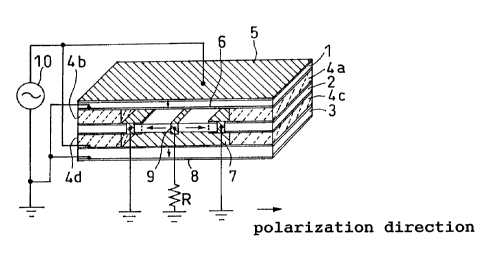
Figs . lA to 1C show a structure of a piezoelectric
transformer of a first embodiment according to the present
invention. The first embodiment is presented to describe a
basic structure of piezoelectric transformers according to
second to seventh embodiments that will be subsequently
described.
Piezoelectric ceramic substrates (each of which will
22
CA 02363659 2001-08-14
hereinbelow referred to as a piezoelectric substrate) 1, 2
and 3 each having a plane plate shape are laminated with
connectors 4a, 4b, 4c, and 4d being sandwiched therebetween
at longitudinal end portions thereof. Adhesive layers (not
shown) are formed on mutually contacting faces of the three
piezoelectric substrates and the connectors. Thus, the
piezoelectric transformer are integrally structured. Air
gaps are formed on opposing portions of the piezoelectric
substrates opposing each other, where the connectors are not
disposed. Mutually opposing electrodes 5 and 6 are formed
on substantially entire portions of two main faces of the upper
first piezoelectric substrate 1, which is one of the three
piezoelectric substrates 1, 2, and 3. Similarly, electrodes
7 and 8 are formed on the lower third piezoelectric substrate
3. In addition, a strip-like electrode 9 extending
perpendicular to the longitudinal direction is formed on a
main face at a longitudinally central portion of the
intermediate second piezoelectric substrate 2.
Hereinbelow, operational principles are described.
First, a description will be made regarding a case where the
first piezoelectric substrate 1 and the third piezoelectric
substrate 3 are set to input section, and the second
piezoelectric substrate 2 is set to an output section. An
alternating current (AC ) voltage waveform having a frequency
23
CA 02363659 2001-08-14
having a longitudinal length of a halfwavelength is applied
to the electrodes 5 , 6 , 7 and 8 provided on the piezoelectric
substrates 1 and 3. The piezoelectric substrates 1 and 3
excite a standing wave having the halfwavelength of a
mechanical vibration resulting from piezoelectric resonance
with the node located at the longitudinal central portion.
A stress distribution and a displacement amplitude
distribution in the above case are shown in Figs.lB and 1C,
respectively.
Then, mechanical vibration energy of the piezoelectric
substrates 1 and 3 is propagated to the second piezoelectric
substrate 2 provided on the substrates via the connectors 4a,
4b, 4c, and 4d. Thereby, longitudinal mechanical stretching
vibrations are generated in a halfwavelength mode. The
mechanical vibration energy is taken out as a high voltage
current stepped up by the electrode 9 according to a
piezoelectric longitudinal effect. The energy is then
applied to a load R.
The voltage variation ratio is determined according
to the ratio between input impedance and output impedance.
Voltage step-down operation can therefore be performed
through changing input and output electrical connectionsfrom
each other.
The above-described piezoelectric transformer of the
24
- CA 02363659 2001-08-14
present invention enables the achievement of high outputs,
high safety, low frequency operation, miniaturization, high
voltage step-up ratios , high efficiency, and high vibrational
stability. These are described hereinbelow in detail.
The first subject is to achieve high outputs. The high
outputs can be achieved for the following reasons . Since the
air gaps are provided, most of the portions of the
piezoelectric substrates set to the input sections are
separated from the piezoelectric substrate set to the output
section. Thereby, on fixed faces of the input sections and
the output section, thermal loss due to the difference in the
material property values related to the mechanical vibration
characteristics can be significantly reduced, and
consequently, thermal generation can be reduced. In addition,
because of the air gaps formed by the connectors provided
between the input section and the output section, since the
per unit volume heat radiation area is increased, cooling
effects are increased. Thus, the piezoelectric transformer
i.s advantageous to generate high outputs.
The second subject is to achieve high safety. With
the connectors provided between the input sections and the
output section, since the air gaps are formed therebetween,
long creeping distances can be secured, and inter input output
dielectric strength can be significantly improved. Thereby,
~
CA 02363659 2001-08-14
inter input output dielectric characteristics can be
prevented from breakdown.
The third subject is to achieve low-frequency
operation. This can be achieved for the following reasons.
Through the connection of the input sections and the output
section via the connectors, the piezoelectric transformer
vibrates in a state where the mass of the output section is
added to vibrators forming the input sections. This causes
reduction in the resonance frequency of the overall mechanical
vibration system that includes the input sections and the
output section. The piezoelectric transformer is thereby
excited to resonantly vibrate at a frequency that is further
lower than that in a case where only the input section is
operated to vibrate. In specific, when the vibration mode
and the device length, which is the longitudinal length, are
fixed to be constant, the piezoelectric transformer can be
operated at an even lower frequency.
The fourth subject is to achieve miniaturization.
According to the above-described structure, when the device
length is constant , the operation can be performed at an even
lower frequency. For this reason, when the operation
frequency is constant, the device length can be made even
shorter. Thus, the piezoelectric transformer is structured
advantageously for miniaturization.
26
- CA 02363659 2001-08-14
The fifth requirement is to achieve high voltage
step-up ratios. As shown in Fig.lA, in the input sections,
the electrodes are provided on the two main faces, and the
strip-like electrode extending in the width direction is
provided in the longitudinally central portion of the output
section. In this structure, the input impedance can be made
lower than the output impedance. In addition, by using a
piezoelectric substrate having a reduced thickness, the
output impedance can be increased. Consequently, design is
can be made easily for the voltage step-up ratio that is
determined according to the square root of the ratio between
the input and output impedances.
The sixth subject is to achieve high efficiency.
Since the piezoelectric transformer is structured as shown
in Fig.lA, either in the input sections and the output section,
electrode external connection portions can be provided at
vibrational node portion. In this case, interference is less
in piezoelectric vibration, thereby allowing high efficiency
to be expected.
The seventh subject is to achieve high vibrational
stability. Since the input electrode is disposed on the
entirety of the main face of the plane-plate-like board,
vibrations in one wavelength mode do not easily occur. This
enables even more stable halfwavelength resonant vibrations
27
CA 02363659 2001-08-14
to be generated.
(Second Embodiment)
Fig.2 is a perspective view of a piezoelectric
transformer according to a second embodiment. The
piezoelectric transformer uses ceramic piezoelectric
substrates obtained by sintering an ordinary PZT material,
which is an ordinary piezoelectric transformer material. A
first piezoelectric substrate 12 and a third piezoelectric
substrate 16 having input sections are connected to a second
piezoelectric substrate 14 having an output section. The
substrates are connected via connectors 13 and 15 that are
formed of a PZT ceramic and are provided in longitudinal end
portions . In this case , contacting faces of the respective
piezoelectric substrates and the connectors are bonded
together by using a thermosetting epoxy adhesive . Thus , the
piezoelectric transformer is integrally structured. Air
gaps are formed in portions where the connectors are not
disposed. The piezoelectric transformer has a size of 30 mm
mm X 5 mm. On two main faces of the first piezoelectric
substrate 12 forming the input section, an electrode 17a and
an electrode 17b are formed to oppose each other. Similarly,
on the third piezoelectric substrate 16 forming the input
section, an electrode 18a and an electrode 18b are formed to
oppose each other. In addition, a strip-like electrode 19
28
CA 02363659 2001-08-14
extending perpendicular to the longitudinal direction is
formed on main faces in a longitudinally central portion of
the intermediate second piezoelectric substrate forming the
output section 14.
The respective electrodes were formed such that Pd-Ag
conductive paste is used, and electrode patterns were formed
thereon according to a screen printing method. Polarization
processing was performed in oil, and thereafter, aging was
performed. In this way, the piezoelectric substrates were
produced.
Each of the upper and lower first and third
piezoelectric substrates 12 and 16 is polarized in the
thickness direction, and the intermediate second
piezoelectric substrate 14 forming the output section is
polarized in the longitudinal direction. However, the
intermediate piezoelectric substrate 14 was formed to have
two regions in the longitudinal direction at the border of
the longitudinally central portion. The two regions were
polarized in mutually opposing parallel directions. The
length of the longitudinal polarization region of the
intermediate piezoelectric substrate 14 was determined
according to conditions for impedance matching with a load
R.
Regions other than the longitudinal polarization
29
~
CA 02363659 2001-08-14
region of the intermediate second piezoelectric substrate 14
are preferably polarized in the thickness direction of the
piezoelectric substrate 14. In this case, when wiring is
performed as shown in Fig.2, each of the areas polarized to
the thickness direction can be operated as a part of the input
section. Also, the connectors 13 and 15 are preferably
polarized parallel to the thickness direction of the
respective piezoelectric substrate.
(Third Embodiment)
Figs.3A and 3B illustrate a piezoelectric transformer
according to a third embodiment. Fig.3A is a perspective view
of the piezoelectric transformer, and Fig.3B is a right side
view thereof. As shown in Fig.3A, the piezoelectric
transformer is formed to include a second piezoelectric
substrate 23 formed by sintering a PZT piezoelectric ceramic
into a monolithic plate, a first piezoelectric substrate 21
and a third piezoelectric substrate 25 that are respectively
formed to have a multilayer structure in which PZT
piezoelectric ceramic layers and electrodes are alternately
disposed in the thickness direction. The aforementioned
substrates are bonded together using a thermosetting epoxy
adhesive together via connectors 22 and 24 respectively formed
of a PZT ceramic. Thus, the piezoelectric transformer is
integrally structured. The direction along which the
CA 02363659 2001-08-14
piezoelectric substrates are connected and laminated is the
same as the overlay direction of the first piezoelectric
substrate 21. Except for the piezoelectric multilayer
structure used for the first piezoelectric substrate 21, the
structure of the piezoelectric transformer of the present
embodiment is similar to that of the second embodiment. In
the present embodiment, the first and third piezoelectric
substrates 21 and 25 are respectively set to input sections,
and a longitudinally central portion of the second
piezoelectric substrate 23 is set to an output section.
In the first and third piezoelectric substrates 21 and
25, an alternating current is input between an electrode group
26 and another electrode group 27 opposing thereto. As shown
in Fig.3B, the electrode group 26 is formed such that inner
electrodes formed between piezoelectric layers in the
lamination direction are alternately electrically connected
through a side face electrode 29' . Each of the piezoelectric
multilayersubstratesispolarized inthethickness direction,
and an each pair of the piezoelectric layers adjacent to each
other in the lamination direction are polarized in mutually
opposing parallel directions. In the multilayer structure
thus fabricated, high voltage step-up ratios can be obtained.
(Fourth Embodiment)
Figs . 4A and 4B illustrate a piezoelectric transformer
31
CA 02363659 2001-08-14
according to a fourth embodiment. Except for the
polarization structure of the second piezoelectric substrate
23 having the output section, the piezoelectric transformer
of the present embodiment is the same as that of the third
embodiment. In the present embodiment, the second
piezoelectric substrate 23 is formed such that an electrode
29 and an electrode 30 are respectively formed on its opposing
main faces at two portions in the longitudinal direction, and
the polarization is set in the longitudinal direction in a
piezoelectric substrate that connects the electrodes 29 and
30. The positions where the electrodes 29 and 30 are formed
are determined according to conditionsfor impedance matching
with the load. The electrodes 29 and 30 may respectively be
provided to be connected to the two main faces and longitudinal
side faces of the piezoelectric substrate.
By providing an electric pattern of the output side,
inter input output electric insulation can be established,
and the piezoelectric transformer has a strong structure
against noise, such as power noise.
(Fifth Embodiment)
Fig.5 shows a piezoelectric transformer of a fifth
embodiment. The present embodiment is different from the
piezoelectric transformer of the second embodiment in the
shapes of the connectors and the position where the electrode
32
~ ~ CA 02363659 2001-08-14
is connected outside from the piezoelectric transformer.
Other portions are similar to those described in the second
embodiment.
In the present embodiment, a connector 31 is formed
to include a portion 31a, which is connected to longitudinal
end portions of respective piezoelectric substrates, and
projecting portions 31b and 31c respectively sandwiched
between two piezoelectric substrates. The projecting
portions 31b and 31c are not only sandwiched between the
respective piezoelectric substrates, but are also shaped to
cover longitudinal end faces of the respective piezoelectric
substrates. Thereby, since vibrations of the input side
piezoelectric substrates can be efficiently transferred to
the output side, the power conversion ratio can be increased.
The position where the electrode is connected to the
outside from the piezoelectric transformer is provided on
longitudinal side faces and at a longitudinally central
portion of the respective piezoelectric substrate. For
example, the structure is fabricated such that an electrode
terminal 32 of the upper piezoelectric substrate is connected
to an electrode 35 on the upper main face, an electrode
terminal 33 is connected to an electrode 36 on the lower main
face, and an input voltage or an output voltage is applied
between the electrode terminals 32 and 33. In this structure
33
~
CA 02363659 2001-08-14
(lower electrodes are not shown), short circuiting can be
prevented through cutouts 34 each provided near a terminal
of opposing electrodes on the upper and lower main faces.
(Sixth Embodiment)
Fig.6 shows a piezoelectric transformer of a sixth
embodiment. The piezoelectric transformer is formed to
include a piezoelectric layer 43 made of a PZT piezoelectric
ceramic sheet, a first piezoelectric substrate 43' on which
inner electrodes 42a and 42b are alternately disposed in the
longitudinal direction, a second piezoelectric substrate 48
similar to the first piezoelectric substrate 43' , and a third
piezoelectric substrate 49. These substrates are connected
together via connectors 46a, 46b, 46c, and 46d each formed
of a PZT ceramic by using a thermosetting epoxy adhesive.
Thus, the piezoelectric transformer is integrallystructured.
The electrode forming method and the polarization method are
similar to those employed in the second embodiment . In each
of the first, second, and third piezoelectric substrates 43' ,
48, and 49, the piezoelectric layer is polarized in the
longitudinal direction, and the piezoelectric layers
adjacent to each other in the longitudinal direction are
polarized to mutually opposite in the parallel direction.
An alternating current is input between an electrode
group 47a and another electrode group. The electrode group
34
~
CA 02363659 2001-08-14
47a is formed such that inner electrodes 42a formed between
the piezoelectric layers in the lamination direction are
alternately electrically connected through a side face
electrode. The aforementioned other electrode group
includes the electrodes 42b in an interior portion opposing
the electrode group 47a. Also the third piezoelectric
substrate similarly operates as an input section. The
electrode groups include electrodes 44a and 44b provided on
their longitudinal end faces.
According to the structure in which the first and third
piezoelectric substrate 43' and 49 are laminated in the
longitudinal direction, piezoelectric longitudinal
resonance having a large electromechanical coupling
coefficient can be used. Thereby, electric energy can be
converted to mechanical vibration energy at an even higher
energy conversion efficiency to cause vibrations. Similarly,
in the structure in which the second piezoelectric substrate
48 set to the output section is structured through lamination
in the longitudinal direction, piezoelectric longitudinal
resonance having a large electromechanical coupling
coefficient can be used. Thereby, mechanical energy can be
converted to electrical vibration energy at a high energy
conversion efficiency to transfer the energy to an electric
load. Since the energy conversion efficiency is high either
, ' CA 02363659 2001-08-14
in the input sections and the output section, the above-
described structure is advantageous to improve the output
level.
(Seventh Embodiment)
Fig.7 shows a piezoelectric transformer of a seventh
embodiment. The piezoelectric transformer is formed to
include a first piezoelectric layer 54 having a multilayer
structure, a second piezoelectric substrate 55 having a
multilayer structure similar thereto, and a third
piezoelectric substrate 56 having a rnultilayer structure
similar thereto. The first piezoelectric layer 54 is formed
such that electrodes are disposed on upper and lower main faces
of a plurality of PZT piezoelectric ceramic sheet alternately
in the longitudinal direction and linearly in the width
direction, and the sheets are sintered to form an integrally
unit. These substrates are bonded together via connectors
each formed of a PZT ceramic by using a thermosetting epoxy
adhesive. Thus, the piezoelectric transformer is integrally
structured.
The above-described structure will be described in
detail with reference to Fig.8. Fig.8 is an exploded view
of the structure wherein the first piezoelectric layer 54 and
the third piezoelectric substrate 56, which are respectively
set to input sections , and the second piezoelectric substrate
36
CA 02363659 2001-08-14
55, which is set to an output section, are each formed of a
piezoelectric sheet formed of three layers. On each of the
piezoelectric sheets, electrode groups 53, 52, 65, 66, and
the like are alternately provided linearly in the width
direction. The respective electrode groups are coated
thereon according to a screen printing method. The
respective piezoelectric sheets are produced through
integral sintering. The piezoelectric substrates for the
input sections are bonded via connectors 67a, 67b, 67c, and
67d by using an epoxy adhesive. After the piezoelectric
substrates are bonded, voltage is applied to inner electrodes,
and interelectrode regions are polarized. The piezoelectric
substrates for the input sections and the output section are
respectively polarized in the longitudinal direction, and the
adjacent regions on the piezoelectric sheets are polarized
in mutually opposing parallel directions. An alternating
voltage is applied between an electrode group and another
electrode group opposing thereto. The electrode group is
formed such that inner electrodes formed between the
respective piezoelectric layers in the lamination direction
are alternately electrically connected through a side face
electrode.
In the structure in which the input section sheets are
laminated in the thickness direction, the polarization
37
CA 02363659 2001-08-14
directions of the interelectrode regions can be set
substantially in parallel to the longitudinal direction.
Thereby, piezoelectric longitudinal resonance having a high
electromechanical coupling coefficient can be caused. In
addition, electric energy can be converted to mechanical
vibration energy at an even higher energy conversion
efficiency to cause vibrations. Similarly, in the structure
in which the output section is laminated in the longitudinal
direction, piezoelectric longitudinal resonance having a
high electromechanical coupling coefficient can be used.
Thereby, mechanical energy can be converted to electrical
vibration energy at a high energy conversion efficiency to
transfer the energy to an electric load. Since the energy
conversion efficiency is high either in the input sections
and the output section, the above-described structure is
advantageous to improve the output level. In addition, the
structure in which the integral sheets are laminated in the
longitudinal direction is advantageous in that the strength
can be increased to resist breakdown due to tensile stress
caused perpendicular to the longitudinal direction when the
structure expands and contracts.
The above-described first to seventh embodiments are
characterized as follows. As shown in Figs.lB and 1C, any
one of the piezoelectric transformers can be operated to
38
CA 02363659 2001-08-14
vibrate in the halfwavelength mode. In this case, since the
connectors are provided in the longitudinal end portions,
which are vibrational loop portions , vibrations of the input
side substrates can be efficiently transferred to the output
side substrate. Depending on the vibration mode, a connector
can be provided in a longitudinally central portion of the
substrate.
Furthermore, in each of the embodiments, description
has been made with reference to the case where the three
piezoelectric substrates are used. However, the third
piezoelectric substrate may be eliminated, and the
configuration may be made with only the first piezoelectric
substrate and the second piezoelectric substrate. Still
furthermore, In addition, four or more piezoelectric
substrates may be laminated via connectors.
Hereinbelow, a description will be made regarding a
method for mounting the piezoelectric transformer according
to one of the above-described first to seventh embodiments
on a printed substrate. Fig.9 illustrates the state of
mounting of a piezoelectric transformer to a printed wiring
board. Similarly to the fifth embodiment, the piezoelectric
substrate has electrode external connection portions at
widthwise end faces of respective piezoelectric substrates
in longitudinally central portions. The external connection
39
CA 02363659 2001-08-14
positions correspond to the vibrational nodes of the
piezoelectric substrates. Portions in these positions can
be used for electrical connection as well as for mechanical
connection, that is, for fixing the piezoelectric transformer.
The two connections can concurrently be implemented by
applying solder between each of the piezoelectric transformer
electrodes and the printed substrate. In the structure shown
in Fig. 9 , electrode terminals 32 , 33 , 37 , 38 , and 39 provided
on the piezoelectric transformer are soldered to electrode
terminals 60 to 64. In specific, soldering is performed for
the respective combinations of 32 and 61, 33 and 60, 37 and
64, 38 and 62, and 39 and 63. In this way, in the structure
in which the piezoelectric transformer is electrically and
mechanically connected to the printed substrate, it can be
directly mounted in a reflow furnace to the printed substrate.
Thereby, the manufacturing cost can be significantly reduced.
As described above, according to the first to seventh
embodiments, high outputs, high safety, low frequency
operation, miniaturization, high voltage step-up ratio, high
efficiency, and high vibrational stability can be achieved.
(Eighth and Ninth Embodiments)
Hereinbelow, eighth and ninth embodiments will be
described. In the eighth embodiment, a basic structure and
' CA 02363659 2001-08-14
operational principles will be described. In the ninth
embodiment, a more practical embodiment will be described.
(Eighth Embodiment)
Fig.lO shows a piezoelectric transformer according to
the eighth embodiment. Rectangular parallelepiped
piezoelectric substrates 101, 102, and 103 formed of a
piezoelectric material are laminated via connectors 104a,
104b, 104c, 104d, 104e, 104f, 1048, and 104h sandwiched
therebetween. The three piezoelectric substrates and the
connectors are integrally bonded through adhesive layers (not
shown) applied on their mutual contacting faces. Air gaps
are formed in portions where the piezoelectric substrates
mutually oppose, and connectors are not disposed.
The three piezoelectric substratesin the longitudinal
direction are equally divided into three regions, and the
connectors are provided on the borders of the regions, and
end portions of the piezoelectric substrates.
A piezoelectric substrate 101 has three divisional
regions in the longitudinal direction. On first faces of the
respective regions, an electrode 105a, an electrode 106a, and
an electrode 107a are formed. On second faces on the reverse
sides of the first faces, electrodes respectively opposing
the electrodes on the first face are formed. The respective
interelectrode regions are polarized perpendicular to the
41
CA 02363659 2001-08-14
faces of the electrodes , and the polarization directions in
the adjacent regions oppose in parallel to each other. The
electrodes 105a, 106a, and 107a are electrically connected
from one another, and the opposing electrodes are electrically
connected from one another, respectively configuring
electrode groups. The piezoelectric substrate 103 is
structured in the same manner as that for the piezoelectric
substrate 101.
The piezoelectric substrate 102 can be divided into
three longitudinal regions. An electrode 108 and an
electrode 111 are respectively formed on longitudinal end
faces of the piezoelectric substrate. Electrodes 109 and 110
are respectively formed on border faces perpendicular to the
longitudinal direction of the regions. The respective
interelectrode regions are polarized perpendicular to the
faces of the electrodes, and the polarization directions in
the adjacent regions are longitudinally perpendicular and
mutually opposite.
Hereinbelow, operational principles will be
described.
Description will be made referring to a case where the
piezoelectric substrates 101 and 103 are respectively set to
input sections, and the piezoelectric substrate 102 is set
to an output section. An electrically connected group of the
42
' CA 02363659 2001-08-14
electrodes 105a, 106a, and 107a provided on the piezoelectric
substrate 101 and three electrodes provided on the
corresponding faces of the piezoelectric substrate 103 is used
as an electrode group A. An electrically connected group of
the electrodes provided in the reverse faces of the
piezoelectric substrates 101 and 103 is used as an electrode
group B. An AC voltage at the frequency having the
longitudinal length of a 1.5 wavelength are applied between
the electrode group A and the electrode group B . As a result ,
since the respective polarization directions in the three
divisional regions of the piezoelectric substrates 101 and
103 are mutually opposite, according to a piezoelectric
transverse effect, the adjacent regions perform stretching
vibrations in the longitudinal direction in mutually opposite
phases , and a standing wave having a 1 . 5 wavelength is excited
in the longitudinal direction. A stress distribution and an
amplitude distribution in the above case are shown in Figs.llA
and 11B, respectively.
Mechanical vibration energy of the piezoelectric
substrate 101 and 103 is propagated to the intermediate
piezoelectric substrate 102 via the connectors 104a, 104b,
104c, 104d, 104e, 104f , 104g, and 104h provided in vibrational
loop portions. Thereby, the piezoelectric substrate 102
performs stretching vibrations with a standing wave having
43
' CA 02363659 2001-08-14
a 1 . 5 wavelength in the longitudinal direction . In this case ,
in the three longitudinally divided regions, the adjacent
regions expand and contract in mutually opposing phases; and
since the polarization directions in the adjacent regions are
longitudinally parallel and mutually opposite, phases of the
voltage generated according to the piezoelectric
longitudinal effect become the same, and stepped-up high
voltage alternating currents can be obtained from the
electrode 111 and the electrode 108.
The transformation ratio is proportional to the square
root of the ratio between input impedance and output impedance.
Therefore, voltage step-down operation can be performed by
changing the input and output electrical connections from each
other.
In the piezoelectric transformer of the present
embodiment, a larger number of piezoelectric substrates may
be connected via connectors , thereby allowing them to be
extended as necessary.
In addition, a number N of longitudinal divisional
regions of the respective piezoelectric substrates is at least
two, and the upper limit is not specifically restricted. In
practice, however, the upper limit is preferably set to 100.
The above-described piezoelectric transformer of the
present invention enables the achievement of high outputs,
44
' CA 02363659 2001-08-14
high safety, low frequency operation, miniaturization, and
high voltage step-up ratios. Hereinbelow, these are
described in detail.
The first subject is to achieve high outputs.
Increasing the volume is effective to achieve high outputs .
According to the present structure, the volume can easily be
increased in the longitudinal direction in units of a 1/2
wavelength without changing the frequency. Furthermore,
because of the air gaps formed by the connectors in the input
sections and the output section, since the per unit volume
heat radiation area is increased, cooling effects are
increased. Consequently, the piezoelectric transformer is
advantageous to generate high outputs.
The second subject is to achieve high safety. With
the connectors provided between the input sections and the
output section, since the air gaps are formed therebetween,
long creeping distances can be secured, and the inter input
output dielectric strength can be significantly improved.
Thereby, inter input output insulation can be prevented from
breakage.
The third subject is to achieve low frequency operation.
This can be achieved for the following reasons. According
to the connection of the input sections and the output section
via the connectors, the piezoelectric transformer vibrates
' CA 02363659 2001-08-14
in a state where the mass of the output section is added to
vibrators forming the input sections . This works to reduce
resonance frequency of the overall mechanical vibration
system including the input sections and the output section.
Thereby, the piezoelectric transformer resonantly vibrates
at a frequency that is further lower than that in a case where
only the input section is operated to vibrate. In specific,
when the vibration mode and the device length, which is the
longitudinal length, are constant, the piezoelectric
transformer can be operated at an even lower frequency.
The fourth subject is to achieve miniaturization.
According to the above-described structure, when the device
length is constant, the operation can be performed at an even
lower frequency. Conversely, when the operation frequency
is constant , the device length can be made even shorter . Thus ,
the piezoelectric transformer is structured advantageously
for miniaturization.
The fifth requirement is to achieve high voltage
step-up ratios. As shown in Fig.lO, in the input sections,
the electrodes are provided on the two main faces, and the
strip like electrode extending in the width direction is
provided in the longitudinally central portion of the output
section. In this structure, the input impedance can be made
lower than the output impedance. In addition, using the
46
' CA 02363659 2001-08-14
piezoelectric substrate having a reduced thickness enables
the output impedance to be increased. Consequently, design
is can be made easily for voltage step-up ratios that are
determined according to the square root of the ratio between
the input output impedances.
In addition to the structure shown in Fig.lO, a number
of structures of the piezoelectric substrates exemplifying
the present invention can be considered. Examples
conceivable structures are described hereinbelow.
(Ninth Embodiment)
Fig. l2 is a perspective view of a piezoelectric
transformer according to a ninth embodiment.
The piezoelectric transformer uses ceramic
piezoelectric substrates obtained by sintering an ordinary
PZT material, which is an ordinary piezoelectric transformer
material. The present embodiment will be described regarding
a case where piezoelectric substrates 121 and 123 are
respectively set to input sections, and a piezoelectric
substrate 122 is set to an output section. To excite a
standing wave having a 1.5 wavelength in the longitudinal
direction for operation, the structure of the present
embodiment is formed such that connectors are inserted in
border portions in three longitudinally divided regions,
which corresponds to vibrational loop portions, and
47
' CA 02363659 2001-08-14
contacting faces of the respective piezoelectric substrates
and the connectors are bonded together by using a
thermosetting epoxy adhesive. Air gaps are formed in
portions where the connectors are not disposed. The
piezoelectric transformer has a size of 30 mm x 10 mm X 5 mm.
The first piezoelectric substrate 121 forming the
input section is formed of a piezoelectric multilayer
substrate in which PZT piezoelectric ceramic sheets and
electrode layers are alternately disposed in the longitudinal
direction. A group in which inner electrodes formed between
the piezoelectric sheets are alternately electrically
connected through a side face electrode 124 is used as an
electrode group 125, and another electrode group 126 opposing
thereto is electrically connected through another side face
electrode.
The polarization directions are longitudinally
parallel and mutually opposite. However, in three
longitudinally divided regions 117, 118, and 119, the two
regions 117 and 119 at the two end portions and the
intermediate region 118 are set to the polarization directions
such that polarities in the polarization directions for
connecting to the electrodes of the electrode group 125 or
126 oppose each other.
According to the above arrangement , when an AC voltage
48
CA 02363659 2001-08-14
is applied from an external source, in the three
longitudinally divided regions 117, 118, and 119, the two
regions 117 and 119 at the two end portions and the
intermediate region 118 vibrate in mutually opposing phases,
and vibrations in a 1.5-wavelength mode is enabled to easily
occur. The third piezoelectric substrate 123 is structured
in the same manner as the piezoelectric substrate 121.
The second piezoelectric substrate 122 forming the
output section is formed of a piezoelectric multilayer
substrate in which PZT piezoelectric ceramic sheets and
electrode layers are alternately disposed in the thickness
direction. Inner electrodes of the piezoelectric multilayer
substrate are equally divided into three regions. In each
of the regions, a group in which the inner electrodes formed
between piezoelectric sheets are alternately electrically
connected through a side face electrode 127 is used as an
electrode group, and another electrode group opposing thereto
is electrically connected through another side face electrode
128. A cutout 129 is provided near an electrode terminal
opposing each of the side face electrodes , thereby enabling
shortcircuiting with the opposing electrode group to be
prevented. The polarization directions in adjacent layers
are set to mutually oppose in parallel.
In addition, side face electrodes of the three regions
49
CA 02363659 2001-08-14
are connected so that polarities in the polarization direction
of the adjacent regions oppose each other. Thereby, when the
piezoelectric substrate is excited at a 1.5 wavelength, since
the two regions at the two end portions and the intermediate
region vibrate in mutually opposing phases, in phase AC
voltages can be output.
The electrodes are formed such that Pd-Ag conductive
paste is used, and electrode patterns are formed thereon
according to a screen printing method.
Polarization is performed in oil, and thereafter,
aging is performed. In this way, the piezoelectric
multilayer substrate is produced.
By reducing the thickness of the multilayer body of
the output substrate, the output impedance can be reduced,
and the value of a matched load can be reduced. Conversely,
by increasing the thickness of the multilayer body, the output
impedance can be increased, and the value of a matched load
can be increased.
Similarly, by changing the thickness of the multilayer
body of the input substrate, the input impedance can be set
to arbitrary value.
In the above, description has been made referring to
the case the piezoelectric substrates are excited at the 1.5
wavelength. However, by extending them in units of 1/2
CA 02363659 2001-08-14
wavelengths, the piezoelectric transformer can be driven in
a 2-wavelength mode or a higher mode.
In addition, in the sate shown Fig. l2, the substrates
of the respective input section and output section may be
connected to each other in a state where each of the substrates
is 90° rotated with respect to a central axis in the
longitudinal direction.
Furthermore, with respect to the configuration of the
ninth embodiment, the piezoelectric substrates can be
arranged in various other modes. Example modes will
hereinbelow be described referring to Figs.l3, 14, 15, and
16. The piezoelectric substrates are each capable of
functioning either as an input section or as an output section.
Thereby, depending on the combination of the piezoelectric
substrates and the connection thereof , design is enabled for
a piezoelectric transformer achieving desired input
impedance and output impedance.
A piezoelectric substrate shown in Fig.l3 is
structured similar to the output section shown in Fig.lO.
That is , the substrate is formed of a multilayer body in which
piezoelectric blocks are laminated with electrodes
sandwiched between the blocks. Electrodes 144, 145, 146, and
147 are formed on end faces and border faces that are
perpendicular to the longitudinal direction in three equally
51
' CA 02363659 2001-08-14
divided regions 141, 142, and 143. The respective
interelectrode regions are polarized perpendicular to faces
of the electrodes. The polarization directions in the
regions adjacent to each other are longitudinally parallel
and mutually opposite.
To control the piezoelectric substrate to function as
an input section, AC voltages are applied to the electrodes
144 and 147. As a result, according to a piezoelectric
longitudinal effect, the regions 141 and 143 vibrate in the
same phase, and the region 142 vibrates in the opposite phase
with respect to the regions 141 and 143, thereby allowing
1.5-wavelength vibrations to be caused.
In addition, to control the piezoelectric substrate
to function as an output section, vibrations are generated
with a 1.5 wavelength. Thereby, the regions 141 and 143
vibrate in the same phase, and the region 142 vibrates in the
opposite phase with respect to the regions 141 and 143. In
this case, the polarization directions in the regions 141 and
143 are identical, and the polarization direction in the
region 142 is opposite to those of the regions 141 and 143.
This enables voltages uniformed in phase to be series
connected and to be taken out from the electrodes 144 and 147
located at the end portions.
The piezoelectric substrate is structured
52
o ' CA 02363659 2001-08-14
advantageously to achieve high input impedance when it is
driven as an input section. Concurrently, the piezoelectric
substrate is structured advantageously to achieve high output
impedance when it is driven as an output section.
A piezoelectric substrate shown in Fig. l4 is formed
of piezoelectric multilayer substrates in which PZT
piezoelectric ceramic sheets and electrode layers are
alternately disposed in the longitudinal direction. A group
in which inner electrodes formed between the piezoelectric
sheets are alternately electrically connected is used as an
electrode group 148, and another group corresponding thereto
is used as an electrode group 149.
The polarization directions in the respective regions
are longitudinally parallel and mutually opposite. However,
in three longitudinally divided regions 150, 151, and 152,
the two regions 150 and 152 located at the two end portions
and the intermediate region 151 are set to the polarization
directions such that polarities in the polarization
directions for making connection to the electrodes of the
electrode group 148 or 149 oppose each other.
To control the piezoelectric substrate to function as
an input section, AC voltages are applied to the electrodes
148 and 149. As a result, according to a piezoelectric
longitudinal effect, the regions 150 and 152 vibrate in the
53
' CA 02363659 2001-08-14
same phase, and the region 151 vibrates in the opposite phase
with respect to the regions 150 and 152, thereby allowing
1.5-wavelength vibrations to be caused.
In addition, to control the piezoelectric substrate
to function as an output section, it is excited with a 1.5
wavelength. Thereby, the regions 150 and 152 vibrate in the
same phase, and the region 151 vibrates in the opposite phase
with respect to the regions 150 and 152. In this case, the
polarization directions of the regions 150 and 152 are
identical, and the polarization direction of the region 151
is opposite to those of the regions 150 and 152. This allows
voltages uniformed in phase to be series connected and to be
taken out from the electrode 148 and 149 located at the end
portions.
The structure of the piezoelectric substrate is
advantageous to achieve low input impedance when it is driven
as an input substrate in the manner of increasing the number
of lamination layers and reducing the thickness of the
multilayer body. Also, the structure is advantageous to
achieve a low output impedance when it is driven as an output
substrate in the same manner as mentioned above.
A piezoelectric substrate shown in Fig. l5 is formed
of piezoelectric multilayer substrates in which PZT
piezoelectric ceramic sheets and electrode layers are
54
CA 02363659 2001-08-14
alternately disposed in the thickness direction. Inner
electrodes of the multilayer substrate are equally divided
in the longitudinal direction into three regions 153, 154,
and 155. In the region 153, a group in which the inner
electrodes formed between piezoelectric sheets are
alternately electrically connected through a side face
electrode 156 is used as an electrode group, and another
electrode group opposing thereto is electrically connected
through another side face electrode 157. A cutout 158 is
provided near an electrode terminal opposing the side face
electrode, thereby enabling shortcircuiting with the
opposing electrode group to be prevented.
The polarization directions in adjacent layers are set
to mutually oppose in parallel.
In addition, side face electrodes of the three regions
153, 154, and 155 are connected so that polarities in the
polarization direction of the regions 153, 154, and 155 oppose
each other. Thereby, when the piezoelectric substrate is
excited with a 1.5 wavelength, since the two regions located
at the two end portions and the intermediate region vibrate
in mutually opposing phases, in phase AC voltages can be output.
In the example shown in Fig.lS, connecting electrodes 159 and
160 are used to connect the region 153 and 155 and the region
154 so that polarities in the polarization directions oppose
CA 02363659 2001-08-14
each other. When the connecting electrodes 159 and 160 are
not provided, the respective regions are independently
connected to loads . Thereby, a multioutput transformer can
be obtained.
A piezoelectric substrate shown in Fig.l6 has a
thicknesswise multilayer structure to realize the
performance equivalent to that of the input sections 121 and
123 of the piezoelectric transformer shown in Fig.l2. A
lamination method therefor may be such that piezoelectric
substrates 161, 162, and 163 are laminated as a green sheet
and are integrally sintered. Alternatively, the
piezoelectric substrates 161 , 162, and 163 may be respectively
sintered and may be bonded together with an adhesive made of ,
for example, polyimide resin or epoxy resin. In addition,
instead of inner electrodes, cross finger electrodes
extending perpendicular to the longitudinal direction may be
formed on the main faces of the piezoelectric substrates 161 ,
162, and 163. A group in which the inner electrodes or the
cross finger electrodes are alternately electrically
connected through a side face electrode 164 is used as an
electrode group, and another electrode group is electrically
connected to a side face electrode. In addition, the
electrodes are equally in the longitudinal direction divided
into three regions 166, 167, and 168.
56
~
CA 02363659 2001-08-14
The polarization directions in adjacent portions of
the respective regions are longitudinally parallel and
mutually opposite to each other. However, in three
longitudinally divided regions 166, 167, and 168, the two
regions 166 and 168 located at the two end portions and the
intermediate region 167 are set to the polarization directions
such that polarities in the polarization directions for
connecting to the electrodes of the same electrode group 164
or 165 oppose each other. In this structure, when an AC
voltage is applied from an external source, in the three
longitudinally divided regions 166, 167, and 168, the two
regions 166 and 168 located at the two end portions and the
intermediate region 167 vibrate in mutually opposing phases,
and vibrations in a 1.5-wavelength mode is enabled to easily
occur.
Because of the lamination of the above-described
piezoelectric substrates in the thickness direction, the
number of lamination layers can be reduced, and the
manufacturing costs can thereby be reduced. In addition,
although breakdown stresses are generated during excitation,
as shown in Fig.4, in the case where the electrodes are
disposed on the faces that are perpendicular to the
longitudinal direction, mechanical strengths of borders
between the electrodes and the piezoelectric substrates are
57
CA 02363659 2001-08-14
low. In this case, breakdown tends to develop from the border
portions. However, when the electrodes are structured as
shown in Fig.l6, borders between the electrodes and the
piezoelectric substrates, of which the mechanical strengths
are low, can be made parallel to the longitudinal direction.
This allows anti-breakdown strengths to be significantly
increased. Thus, the structure is advantageous to achieve
high outputs.
As described above, the eighth and ninth embodiments
enable the achievement of high outputs, high safety, low
frequency operation, miniaturization, and high voltage
step-up ratios.
In each of the above-described piezoelectric
transformers, the portions for electrically connecting to the
outside are preferably positioned at the nodes of
piezoelectric resonance of the piezoelectric transformer to
prevent the mechanical vibrations from interference. An
electrical connection is preferably made by providing, for
example, a flexible substrate or an electrically conductive
elastic material that uses solder, lead wire, and insulating
material such as polyimide resin, and the like, between the
electrodes positioned at a vibrational node and an external
circuit.
The piezoelectric transformer is supported at node
58
~
CA 02363659 2001-08-14
portions by using an elastic material such as a silicon
adhesive. The piezoelectric transformer according to one of
the first to seventh embodiments is supported at a central
portion in the longitudinal direction by using an elastic
material such as a silicon adhesive. Components can be
reduced in number by using solders, which have been used for
electrical connection, for mechanical connection. This
eventually results in cost reductions. Furthermore, since
the structure allows the electrical connection as well as
mechanical connection to be made to the printed substrate,
direct mounting can be performed on the printed substrate in
a reflow furnace, thereby enabling manufacturing costs to be
reduced.
Still furthermore, by changing the electrical
connections, the described piezoelectric transformer can
also be used either for stepping up the voltage or for stepping
down the voltage. Figs.lA to 7, 10, and 12 each show the
electrical connections for stepping up the voltage; however,
the transformer can also be used for stepping down the voltage
when the inputs and the outputs are reversed. The reversed
connections of the inputs and the outputs would be able to
be presented by reversing the relative descriptions in the
respective embodiments.
In each of the first to ninth embodiments, the end
59
CA 02363659 2001-08-14
portions in the longitudinal direction of the respective
piezoelectric substrates and the border between the
respective polarization regions correspond to the
vibrational loop portions when the piezoelectric transformer
is driven.
(Tenth and Eleventh Embodiments)
Hereinbelow, tenth and eleventh embodiments will be
described. In the embodiment, a basic structure and
operational principles will be described; and in the eleventh
embodiment, a more practical embodiment will be described.
(Tenth Embodiment)
First, operational principles of the tenth and
eleventh embodiments will be described with reference to
Figs.l7A and 17B. Fig.l7A is a schematic perspective view
for explaining a structure of a piezoelectric transformer
according to the present embodiment. As shown in Fig.l7B,
the piezoelectric transformer is formed of a piezoelectric
ceramic, and has a structure in which plane-plate-like
piezoelectric substrates 201, 202, and 203 on which electrodes
201a, 202a, and 203a (only the electrodes on one face are
shown) are formed, respectively are connected by a ring-like
connector 204. Adhesive layers (not shown) are formed on
mutually contacting faces, and the entirety is integrated.
CA 02363659 2001-08-14
Hereinbelow,operational principles will be described.
Description will be made referring to a case where the
intermediate piezoelectric substrate 202 is set to an output
section, and the piezoelectric substrates 201 and 203 provided
on upper and lower portions thereof are respectively set to
input sections. AC voltage waveforms having frequencies for
causing primary order radially expanding vibrations are
applied in the same phase to the disc substrate section formed
on the almost entire face of the circular main faces of the
piezoelectric substrate 201 and 203 of input section 201 and
203 so that the phases of the radially expanding vibrations
of the two input substrates 201 and 203 match. According to
electromechanical coupling, piezoelectric resonance having
a vibrational node corresponding to the center of the main
face is generated on each of the piezoelectric substrates 201
and 203. The states of the vibrations are illustrated in
Figs.l8A to 18D. The respective piezoelectric substrates
repeat expansion and contraction according to basic radial
vibrations as shown in Figs.l8A and 18B. Figs.l8C and 18D
show a displacement distribution and a stress distribution,
respectively, in the radially expanding direction of the basic
radial vibration. As shown in Fig. 18C, the loop portion where
vibrations with a large displacement occur corresponds to the
outer peripheral edge portion of the main face of the
61
' CA 02363659 2001-08-14
piezoelectric substrate, and the node portion where the
displacement in the radial direction is smallest corresponds
to the center of the main face of piezoelectric substrate.
In this case, as shown in Figs.l7A and 178, when the
piezoelectric substrates set to the input sections and the
piezoelectric substrate set to the output section are
connected together via the connector, vibrations of the input
sections can be effectively transferred to the output section.
In the output section, according to radial expansion
electromechanical coupling, the mechanical vibration energy
is converted to electrical vibrational energy, and the energy
is output from the electrodes provided on the main faces of
piezoelectric substrate 202. Air gaps are respectively
formed in central portions in which the connectors do not exist
and which greatly contributes for power generation. In this
structure, vibrations in the thickness direction are not
interfered.
To immobilize the above-described piezoelectric
transformer, fixing fittings are connected to the central
portions that correspond to the radially expanding
vibrational nodes. Thereby, the piezoelectric transformer
can be supported and immobilized without interference being
caused for mechanical vibrations.
Hereinbelow, a description will be made regarding
62
' CA 02363659 2001-08-14
piezoelectric transformers using higher order radially
expanding vibrations. Fig. l9 is a vertically exploded view
of a piezoelectric transformer using a third order mode of
vibration. Piezoelectric substrates 201 and 202 are
connected via two ring-like connectors 206a and 206b.
Similarly, a reverse face of the piezoelectric substrate 202
and the piezoelectric substrate 203 are connected via the
connectors 207a and 207b. Electrode pairs 201a, 201b, and
201c ( the figure shows only one side faces ) mutually opposing
are formed on two circular main faces of the respective
piezoelectric substrates. In a case where the piezoelectric
substrates 201 and 203 are respectively set to input sections,
and piezoelectric substrate 202 sandwiched therebetween is
set to an output section, input AC voltage is applied between
the respective electrode pairs of the piezoelectric
substrates 201 and 203 , and output voltage are taken out from
the electrode pair of the piezoelectric substrate 202.
Figs.20A to 20D show states of a third-order-mode
radially expanding vibrations. The piezoelectric substrate
excited to vibrate in the aforementioned mode repeats
expansion and contraction as shown in Figs.20A and 20B.
Radial distributions in the displacement and stress in this
case are shown in Figs . 20C and 20D, wherein vibrational loop
portions and node portions are formed. In the illustrated
63
CA 02363659 2001-08-14
example, two connectors are positioned in two loop portions
in the radial direction of the vibration, thereby enabling
the vibration to be effectively transferred from the input
section to the output section.
In this way, the number of the connectors is determined
corresponding to the number of orders of the radially
expanding vibrations, and the determined number of the
connectors are provided in the loop portions that are
determined according to the number of orders . Use of the high
mode enables the driving frequency to be increased in the shape
being maintained unchanged.
The ring-like connectors may be dimensioned so that
they can be connected in the positions of the vibrational loop
portions of the respective piezoelectric substrates. The
positions of the vibrational loop portions of the
piezoelectric substrate are determined according to factors,
such as driving frequency, the dimensions of the piezoelectric
substrate, and material property values of the piezoelectric
material.
According to the disposition of each of the connectors
in a ring or ring-like state, compared to a circular connector,
interference is not caused for vibrations in the thickness
direction in the center of the circle where the power
generation efficiency is high. Thereby, a transformation
64
. ' CA 02363659 2001-08-14
ratio substantially as designed can be obtained. For the
material of the connectors, either a conductive material or
a dielectric material may be used. With a connector made of
the dielectric material, the contacting area between the
electrode and the connector disposed in a ring or ring-like
state is small. In this case, since the inter input output
capacitive coupling is reduced, a significant amount of noise
propagating through capacitive coupling can be cut off.
In connection with the connectors respectively
disposed in a ring or ring-like state, an additional advantage
was found in that the element resonance frequency is reduced.
The frequency is considered to decrease because the output
section and the input section are added to each other as a
mass that is added to the system of mechanical resonance, and
the frequency of the system of mechanical resonance is thereby
reduced. The resonance frequency can be adjusted in a range
by changing the width of the ring or ring-like portion.
The respective piezoelectric substrates and
connectors may be connected in a manner that each of the
connectors is integrally sintered using a ceramic material.
In addition, in the structure shown in Figs.l7A and
17B or Fig.9, although three piezoelectric substrates are
connected via the connectors, the piezoelectric substrates
and connectors may be increased in number in the thickness
CA 02363659 2001-08-14
direction. In this case, the piezoelectric substrates
forming the input sections and the output section are
preferably disposed mirror symmetric with respect to a virtual
symmetry plane positioned in the intermediate value in the
thickness direction. Furthermore, according to the increase
in the number of the piezoelectric substrates, a single
input/multiple output transformer can be obtained.
(Eleventh Embodiment)
Fig.21 is a perspective view of a piezoelectric
transformer according to the eleventh embodiment. The
present embodiment will be described referring to a case where
piezoelectric substrates 210 and 212 are respectively set to
input sections, and a piezoelectric substrate 211 is set to
an output section. Each of the piezoelectric substrates 210
and 212 is formed as a circular plate made of a PZT
piezoelectric material, which is an ordinary piezoelectric
transformer material, and disk electrodes 210a, 212a, and so
forth are formed on the upper and lower surfaces of the
piezoelectric substrates. The electrodes are formed such
that Pd-Ag conductive paste is used, and electrode patterns
are coated thereon according to a screen printing method and
are sintered. The output section is formed of the
piezoelectric substrate 211 that is made of the same
piezoelectric material as the input section and that has a
66
' CA 02363659 2001-08-14
structure in which plural electrode layers and plural disk
piezoelectric layers made of a piezoelectric material are
alternately laminated in the thickness direction. Each of
the piezoelectric substrates for the input sections is
polarized so that the polarization axis extends perpendicular
to the upper and lower surfaces . The piezoelectric substrate ,
which is the piezoelectric multilayer body for the output
section, is polarized perpendicular to the upper and lower
surfaces, and adjacent piezoelectric layers therein are
polarized in mutually opposing parallel directions. In the
multilayer structure fabricated as described above, the
output impedance can be reduced, and the transformation ratio
can be increased. In the structure, the output section is
disposed between the two input sections; each of the ring-like
connectors , which is formed of a PZT ceramic material between
the piezoelectric substrate and the piezoelectric multilayer
body, is disposed on the outer peripheral portion
corresponding to the vibrational loop portion; and the
respective contacting faces are bonded together with an
adhesive such as a thermosetting epoxy adhesive or a polyimide
adhesive. The piezoelectric transformer thus structured is
20 mm in diameter and 4 mm in width.
In the output section, the plural electrode layers are
alternately electrically connected, and outputs are taken out
67
' CA 02363659 2001-08-14
through lead wires 216 and 217. In the input section, the
electrodes formed on the mutually opposing faces of the two
piezoelectric substrates 210 and 212 are connected through
a lead wire 215, and alternating currents are applied on the
electrodes on the outer end faces through lead wires 218 and
219 from power supplies . Thus , when the input substrates are
series connected in capacity, the input impedance can be
increase. When the two input substrates are parallel
connected using a different connecting method, the input
impedance can be reduced. The voltage step-up ratio is
proportional to the square root of the ratio between the input
impedance and the output impedance . When the substrates are
electrically connected as shown in Fig.2l, the input impedance
is increased higher than the output impedance, thereby
enabling voltage step-down operation to be performed. When
the input and output connections are reversed, the input
impedance is reduced lower than the output impedance, thereby
enabling voltage step-up operation to be performed.
In addition, in the piezoelectric transformer of the
present embodiment, the outside diameters of connectors 213
and 214 are smaller than the outside diameters of the
piezoelectric substrates 210 and 212 and the outside diameter
of the piezoelectric substrate 211 , which is the piezoelectric
multilayer body. Thereby, the peripheral end faces of the
68
' CA 02363659 2001-08-14
connectors are indented from the outer peripheries of the
input and output substrates, thus forming stepped portions
on the side faces . In this structure, per unit volume surface
area is enlarged, thereby enabling heat radiation effects to
be increased. Furthermore, since the electrodes are coated
with resin, such as epoxy resin or polyimide resin, which has
a high anti dielectric breakdown voltage property, the
creeping distances between the input electrodes and the output
electrode can be increased, and consequently, the anti
dielectric breakdown voltage can be significantly increased.
For the material of the connectors, resin, such as
epoxy resin or polyimide resin, which has high rigidity may
be used. The plural piezoelectric substrates to be used as
described above are set on molds of an injection molding
machine, and in that state, the resin is subjected to injection
molding. Thereby, the components for the transformer can be
easily manufactured. In addition, since the insulation
material is used for the connectors , the region between the
input and the output can be insulated in terms of direct
current.
Example connector structures are shown in Figs . 22A to
22D. In the present invention, the connector used between
the piezoelectric substrates is not limited to be of a
continuous ring as shown in Fig.22A. As shown in Fig.22B,
69
' CA 02363659 2001-08-14
22C, or 22D, the connector may be of a discontinuous ring type,
which isformed of segments disposed circular. The connector
thus formed functions similar to the connector of the
continuous ring type.
When the discontinuous ring type connector as shown
in Fig.22B, 22C, or 22D, is used, the structure allows air
to flow in an fir gap surrounded by the connector. Thereby,
the structure enables the prevention of, for example, an
incident where the piezoelectric transformer generates heat
that can cause rise in interior gas pressure, thereby peeling
off adhesive layers and causing breakdown of the connector.
In addition, when air flows from the outside into the air gap
created by the connectors between the respective
piezoelectric substrates, cooling effects increase in the
internal air gaps , thereby enabling the maximum output power
regulated by temperature rise to be increased.
Figs.23A to 23D, 24A, 24B, 25A, 25B, 26A and 26B show
various modified piezoelectric substrates usable to form the
input substrate or output substrate according to the present
embodiment. Each of the piezoelectric substrate as
illustrated may be used for either the input section or the
output section. Through combination of the illustrated
piezoelectric substrates, a transformer having various input
and output impedance ratios can easily be manufactured.
CA 02363659 2001-08-14
Fig.23A shows a piezoelectric substrate structured
such that electrodes 221a and 221b are provided on two main
faces of a disk piezoelectric substrate 220, the polarization
is directed perpendicular to the electrode faces. Fig.23B
shows a piezoelectric substrate characterized by having a
structure wherein plural piezoelectric layers 220a, 220b, and
220c made of a piezoelectric material and the electrode layers
222a, 222b, 222c, and 222d are alternately laminated in the
thickness direction. In the structure, the aforementioned
plural electrodes are alternately electrically connected,
and electrode layers mutually adjacent therein are insulated
in terms of direct current. The polarization direction is
perpendicular to the disk, and the polarization directions
in piezoelectric layers mutually adjacent are mutually
opposite in parallel. With the aforementioned piezoelectric
multilayer body being used, the electrostatic capacity can
be increased, thereby enabling impedance reduction to be
implemented. Piezoelectric substrates shown in each of
Figs.23C and 23D are structured through modification of the
respective piezoelectric substrates in the disk shape shown
in Figs.23A and 23B to be square. With the modification in
the shape, when they are mounted as electronic components,
dead space can be reduced. Thereby, the mounting space can
be effectively used. In addition, the per unit volume heat
71
CA 02363659 2001-08-14
radiation area is larger than in the case of the disk like
piezoelectric substrate.
Fig.24A is a perspective view showing an example
piezoelectric substrate having an electrode configuration
that enables high order mode excitation, and Fig. 24B is a cross
sectional view thereof. A circular electrode 226b and an
electrode 226a surrounding it are formed on each of upper and
lower main faces of a piezoelectric substrate 225. The border
between the two electrodes is positioned at an loop portion
of a high order mode radially expanding vibration to thereby
enable high order mode radially expanding vibrations to be
generated. The polarization directions are mutually
opposite in parallel in the thickness direction in a circular
and cylindrical region between the two upper and lower
ring-like electrodes 226b and in a circular and cylindrical
region between the two upper and lower ring-like electrodes
226a. In addition, the electrodes positioned on the same main
face are electrically connected through a conductor 229 ,
thereby enabling the number of electrode external connection
portions to be reduced.
In a piezoelectric substrate formed of a piezoelectric
multilayer body as shown in Figs . 25A and 25B, instead of the
piezoelectric body shown in Figs.24A and 24B, piezoelectric
layers 227a, 227b, and 227c and electrode layers 231a and 231b
72
' CA 02363659 2001-08-14
are alternately laminated. In addition, a circular electrode
228b and an electrode 228a surrounding it are formed on each
of upper and lower main faces of the piezoelectric multilayer
body. In the fabrication of the above, as shown in Fig.25B,
the polarization directions of regions adjacent to each other
in the vertical and horizontal directions are set so as to
be mutually opposite in parallel. Thereby, electrical
connection can be carried out from the end face of the disks
adhered to each other as described above . The piezoelectric
multilayer body can also be fabricated through the adhesion
of piezoelectric substrates 225 shown in Figs.24A and 24B.
In each of piezoelectric substrates shown in Figs . 26A
and 26B, the polarization is established in the in plane
direction, and concurrently in the radial direction from the
center. In the piezoelectric substrate shown in Fig.26A, a
circular electrode 233 in provided in a central portion of
a piezoelectric substrate 232 , and a ring-like electrode 232a
is provided in an outer peripheral side portion. In the
polarization direction, polarization axes radially extend in
the region from the circular to the ring-like electrode. In
this arrangement, the electrostatic capacity can
significantly be reduced, and a substrate having a high
impedance value can therefore be easily designed. The
piezoelectric substrate shown in Fig.26B is made to operate
73
' CA 02363659 2001-08-14
even with high order mode radially expanding vibrations . In
addition to a circular electrode 236 and a ring-like electrode
234a provided on a main face of a piezoelectric substrate 234,
a second ring-like electrode 235 is provided in an loop portion
of radially expanding vibration. The piezoelectric
substrate is polarized in the in plane direction and
concurrently in the radial direction from the center. The
polarization direction between the center and the second
ring-like electrode opposes the polarization direction
between the second ring-like electrode and the ring-like
electrode 234 in the outer peripheral portion. In each of
the piezoelectric substrates shown in Figs.26A and 26B, the
ring-like electrode 232a or 234a formed in the outer
peripheral side portion may instead be formed on the main face
of the piezoelectric substrate.
As described above, according to the tenth and eleventh
embodiments , a piezoelectric transformer can be provided in
which high efficiency, high electric power, and
transformation ratios as designed can be obtained, and the
resonance frequency can be reduced. Furthermore, with a
dielectric being used for the connectors, electrostatic
capacity between the input and the output is reduced, thereby
enabling noise propagation to be cut off.
74
~
CA 02363659 2001-08-14
(Twelfth and Thirteenth Embodiments)
Hereinbelow, twelfth and thirteenth the embodiments
will be described.
First, operational principles of the twelfth and
thirteenth embodiments will be described with reference to
Fig.27. Fig.27 is a schematic perspective view for
explaining structures according to the twelfth and thirteenth
embodiments. Circular electrode layers 306, 307, and 308 are
formed on main faces of the respective plane-plate-like
piezoelectric substrates 301 , 302 , and 303 , which are formed
of a piezoelectric ceramic material ( electrodes on the reverse
faces are not shown). The piezoelectric substrates 301, 302,
and 303 are laminated with connectors 304 and 305 being
sandwichedtherebetween. The three piezoelectric substrates
and the two connectors are integrated through adhesive layers
formed on mutually contacting faces thereof.
Hereinbelow,operational principles will be described.
Description will be made referring to a case where the
intermediate piezoelectric substrate 302 is set to an input
section, and the piezoelectric substrates 201 and 203 provided
on outer portions thereof are respectively set to output
sections. AC voltage waveforms having frequencies for
causing primary order radially expanding vibrations are
applied to the circular electrode layers provided on the
' CA 02363659 2001-08-14
obverse and reverse main faces of the piezoelectric substrate
302. According to a piezoelectric transverse effect,
piezoelectric resonance having a vibrational node
corresponding to the center of the plane plate is generated.
In a manner similar to the above, piezoelectric resonance
having a vibrational node corresponding to the center of the
plane plate is generated in the piezoelectric substrate of
the output section through the circular connector. The
mechanical vibration energy is converted to electrical
vibrational energy according to a piezoelectric transverse
effect, and the energy is output.
The transformation ratio is proportional to the square
root of the ratio between the input impedance and the output
impedance. In the present embodiment, since the input
impedance is higher than the output impedance, operation as
a voltage step down transformer can be performed.
The present invention as described above enables inter
input output electrical insulation. In specific, when the
structure is used, since the connectors made of the insulating
material is inserted between the inputs and the output, the
inter input output electrical insulation is enabled:
Furthermore, since the surface area is large, the heat
radiation effects are increased, and high electric power can
thereby be output.
76
CA 02363659 2001-08-14
(Twelfth Embodiment)
Hereinbelow, referring to Fig.27, a piezoelectric
transformer according to the present embodiment will be
described. In the piezoelectric transformer of the present
embodiment , an input section is formed of a square plane plate
made of a PZT piezoelectric material, which is an ordinary
piezoelectric transformer material. On upper and lower faces
of the square plane plate, there are formed circular
electrodes such as to be inscribed on peripheral sides of the
square plane plate by using a Pd-Ag conductive paste according
to a screen printing method. An output section is formed of
the same piezoelectric material as for the input section, and
the electrodes also are formed similar to those of the input
section. Polarization processing is performed for the
respective plane plates so that polarization axes therein are
directed perpendicular to the plane plates. The input
section is disposed between the two output sections , disk-like
connectors made of a PZT ceramic material are disposed between
the plane plates. Mutually contacting faces of the plane
plates and the connectors are bonded using a thermosetting
epoxy adhesive. In this way, the piezoelectric transformer
is structured. With the aforementioned insulating materials
being inserted, inter input output electrical insulation is
enabled. The piezoelectric transformer has a size of 24 mm
77
CA 02363659 2001-08-14
X 24 mm X 4 mm. The voltage step-up ratio is proportional
to the square root of the ratio between the input impedance
and the output impedance. In the embodiment shown in Fig.27,
input voltages are applied to obverse and reverse electrode
layers of the piezoelectric substrate 302 ; and in the output
side, the electrode layer 306 on the obverse side of the outer
piezoelectric substrate 301 is electrically connected to the
electrode 308 on the obverse side of the piezoelectric
substrate, reverse face electrode layers (not shown) are
thereby electrically connected together, and they are
connected to a load 321. Thereby, voltage step-down
operation can be performed. When the connections of the input
and the outputs are reversed, voltage step-up operation can
be performed. For the inter electrode layer connections, the
electrode layers having the same polarity of the piezoelectric
substrate polarization may be electrically connected
together.
(Thirteenth Embodiment)
Fig.28 is a perspective view of a structure wherein
output sections of a piezoelectric transformer according to
the present embodiment are laminated. The present embodiment
is the same as the embodiment 12 except for the configuration
of the output sections. The output sections of the
piezoelectric transformer according to the present
78
~
CA 02363659 2001-08-14
embodiment are formed of laminated piezoelectric substrates
311 and 313. The respective piezoelectric substrates are
formed of square piezoelectric plates 311a, 311b, 313a and
313b made of a PZT piezoelectric material, which is an ordinary
piezoelectric transformer material. On the obverse and
reverse faces of the piezoelectric plate and between the
piezoelectric plates , disc electrode layers 316 , 317 , and 318
are formed such as to respectively be inscribed on peripheral
sides of the square plane plates (electrode layers on the
reverse faces and inner electrodes are not shown). These
electrode layers are formed by using a Pd-Ag conductive paste
according to a screen printing method. On end faces of the
piezoelectric substrates 311 and 313, connection terminals
319 and 320 of the inner electrodes are formed. The
polarization directions of the piezoelectric plates of the
output sections are perpendicular to the main faces of the
piezoelectric plates, and the polarization directions of the
piezoelectric plates adjacent to each other are mutually
opposite in parallel.
In the piezoelectric transformer of the present
embodiment, in the electrodes provided on the piezoelectric
substrate 311, a group in which two electrode layers
alternately formed on the obverse and reverse main faces of
the piezoelectric substrate 311 is used as a first electrode
79
. - CA 02363659 2001-08-14
group. An inner electrode provided between piezoelectric
plate 311a and 311b while it is only one electrode layer is
used as a second electrode group. The respective first
electrode group and the second electrode group are used as
the output sections. The arrangement similar to the above
is made for the piezoelectric substrate 313. The first
electrode groups of the upper and lower piezoelectric
substrates 311 and 313 are electrically connected together,
and are used as one of the output electrodes . Similarly, the
second electrode groups are electrically connected together,
and are used as the other one of the output electrodes . The
output electrodes thus arranged are then connected to a load
321.
In the present embodiment, since the piezoelectric
substrates 311 and 333 are connected to be a multilayer
structure, the impedance thereof is reduced. In this case,
the voltage step-up ratio and the voltage step-down ratio can
be increased.
As described above, according to the above-described
twelfth and thirteenth embodiments, high electric power can
be output , and inter input output electrical insulation can
be established.
In each of the piezoelectric transformers according
, ~ CA 02363659 2001-08-14
to the present invention, to prevent electric discharge to
the interelectrode portion of the output electrode and the
adjacent input section, a high voltage resisting resin film,
such as polyimide resin film, may be inserted in the inter
input output air gap. Alternatively, vanish made of a silicon
adhesive, an epoxy adhesive, or polyimide resin may be applied
therein.
In each of the above embodiments , description has been
made regarding the case where the piezoelectric substrates
and the connectors are connected using adhesives. However,
the connections can be obtained in a way in which ceramic
materials are used for forming the piezoelectric substrates
and the connectors , and the connectors and the piezoelectric
substrates are integrally sintered in the step of sintering
of the piezoelectric substrate. In this case, the connectors
are preferably polarized perpendicular to the main faces of
the piezoelectric substrate. Alternatively, the connectors
may be formed of an adhesive having a high rigidity.
INDUSTRIAL APPLICABILITY
As described above, according to the present invention,
a piezoelectric transformer generating higher output can be
obtained.
As a result , the present invention can preferably be
81
CA 02363659 2001-08-14
utilized especially for a piezoelectric transformer used in
a power converter, such as an inverter for a backlight of a
liquid display and a DC-DC converter.
82