Note: Descriptions are shown in the official language in which they were submitted.
CA 02363663 2001-11-22
DIRECT CONVERSION FLAT PANEL X-RAY DETECTOR
WITH AUTOMATIC CANCELLATION OF GHOST IMAGES
BACKGROUND OF THE INVENTION
Field of the Invention
This invention relates to a structwe of a direct conversion flat panel X-ray
detector that provides for automatic cancellation of ghost images. More
particularly,
the invention relates to an X-ray image flat panel detector comprising a
direct X-ray
to charge converter, a readout thin film transistor array and a transparent
substrate, in
which the after image or ghosting effect, due to charge trapping within the
charge
converter, is automatically and instantly suppressed by a provision of a layer
of
luminophor on the rear of the substrate.
2. Description of the Prior Art
During the last 15 years, many efforts have been directed towards the
development of digital detectors for X-ray imaging. These detectors benefit
from a
much wider dynamic range and improved detection efficiency than film, allowing
for
much better imaging quality. These emerging detectors can be divided into two
groups, one group where the X-rays are converted into light photons which are
then
detected by a light sensitive device i.e. luminophor screen + photodiodes or
charge
coupled device (CCD), and the other group where the X-rays are directly
converted
into electric charges, i.e. direct detection by a semi-conductor such as
silicon,
germanium, cadmium telluride, thallium bromide or amorphous material like
selenium.
The use of selenium as a direct converter, meaning direct generation of
-1-
CA 02363663 2001-11-22
electrical charges under X-ray exposure, simplifies the structure of the
detector
leading to substantial improvement in production yield and cost. It also has
performance advantages such as resolution and sensitivity. Nevertheless, the
collection of these electrical charges requires the use of substantial
electric fields and
can be incomplete because of trapping effects leading to image retention and
ghosting. As described in U.S. Patent No. 5,880,472 by Bradley Trent Polischuk
and
Alain Jean, the selenium direct converter has a multilayer structure
consisting of "p",
"i" and "n" layers. The "p" and "n" layers are no more than a few micrometers
thick;
their role is to block the injection of electrons and holes respectively,
allowing for a
low dark current under high voltage polarization. The X-ray-to-charge
conversion
takes place in the thick "i" layer. The ghosting effect results from charges
captured in
and released from traps located within the "i" selenium converter material as
well as
in the interfaces of the "pin" structure. Each nap is associated with a
charging and
discharging time depending on its energy depth within the amorphous selenium
energy gap between a conduction band and a valence band or within trap states
located in the "ip" and "ni" interfaces. Shallow traps with release time less
than a few
microseconds are insignificant (< 0.5 eV). Deep traps (about >0.7 eV) which
release
their charges within a very long time can build up a residual background image
which
will be detrimental to applications in which switching from intense to low X-
ray flux
is required, such as in angiography applications.
In indirect converters, most of the after image effect is the result of light
emission variations over the emitting surface of the scintillator. It
translates into a
background non-uniformity which can be instantly compensated for by the
addition of
an offset in the processing of the image.
-2-
CA 02363663 2001-11-22
In direct converters, such as those using selenium, a significant part of the
after image is the result of sensitivity variations under the effect of
trapped charges.
Such trapped charges whether in the "in" interface, "pi" interface or in the
bulk of the
"i" layer, tend to locally modify the electric field profile and thus to
change the
collection rate. It results in a gain variation and can only be corrected for
electronically by tedious and time consuming multiplication operations over
the
entire array.
In U.S. Patent No. 5,132,541 by Conrads et al. entitled "Sensor Matrix", a
direct converter flat panel detector of a similar structure is described.
Nevertheless,
the charge trapping effect is ignored and no correction method is proposed.
In U.S. Patent No. 5,396,072 by Schiebel et al. entitled "X-Ray Image
Detector" a direct converter flat panel detector is again described showing
ways to
avoid capacitance coupling with the collecting leads. There is no mention of
image
ghosting nor of ways to avoid image retention by charge trapping.
In U.S. Patent No. 5,880,472, already mentioned above, a selenium multilayer
structure allowing real time imaging capabilities is disclosed. However, no
indication
of the level of image retention or of the means by which this effect can be
eliminated
is given.
In U.S. Patent No. 6,078,053 by Adam et al., an X-ray image erasure method
is disclosed according to which ghost images are erased by simultaneous
application
of high voltage and light to the X-ray imaging device. However, it provides no
automatic cancellation of such ghost images by the actual structure of the
device.
Finally, in a paper by Lee D.L., Cheung L.K., and Jeromin L.S., entitled "A
New Digital Detector for Projection Radiography", 1995, SPIE Vol. 2432, pp.
237-
-3-
CA 02363663 2001-11-22
249, a direct conversion selenium based thin film transistor (TFT) imaging
system is
disclosed where a burst of light is triggered to reset the panel after
readout, once the
high voltage has been switched off. However, this technique, required only to
cancel
the stored image signal, though it may simultaneously release trapped charges,
suffers
from the fact that it cannot be used for real time imaging applications, such
as in
angiography.
There is thus a need for a structure that would provide automatic cancellation
of ghost images in direct conversion detectors.
OBJECTS AND SUMMARY OF THE INVENTION
. It is an object of the present invention to design a structure of a flat
panel
direct conversion X-ray detector that provides for automatic cancellation of
ghost
images.
Another object of the present invention is to apply such structure to selenium
flat panel X-ray detectors.
Other objects and advantages of the invention will be apparent from the
following description thereof.
The present invention uses the incomplete X-ray absorption and subsequent
partial transmission of the converter layer of the flat panel detector, such
as an
amorphous selenium layer, and of its substrate, to stimulate a luminophor
provided on
the back of said substrate. It uses as well the light emitted by the
luminophor and
transmitted through the TFT array built on the glass or other transparent
substrate to
reach the selenium "pin" structure and release the trapped charges. More
specifically,
as the non-absorbed X-ray beam impinges on the luminophor located on the rear
of
the transparent substrate, light is generated, which, by transmission through
the TFT
-4-
CA 02363663 2001-11-22
array, instantly inhibits any trapping of charges, preventing any subsequent
alteration
of the electric field topography and thus the ghosting effect. Moreover, the
trap
inhibition process is self controlled. Indeed, if the trapping increases
locally as a
result of increased X-ray flux, the generated light intensifies and the de-
trapping rate
increases. To be efficient, the light spectrum emitted by the luminophor
should match
the absorption spectrum of the traps. Taking into account the energy gap of
amorphous selenium, the depth of the traps and the energy level of the
interface states
of the "pin" structure, the wavelength of the luminophor will normally extend
from
580 nm to 620 nm. To provide for a minimum transmission through the TFT array,
it
is desirable that its architecture comprise pixel pads and electrodes made out
of
transparent conductors such as Indium Tin Oxide (ITO) or that the fill factor
of the
pixels be partial in order to allow light to flow through the voids. A fill
factor of 70%
is about the best that can be achieved in current TFT technology process. It
allows up
to 30% of the light generated by the luminophor to reach the selenium
structure,
which is sufficient when using a luminophor of average conversion effciency.
It is already known to use a luminophor for improved recording of X-ray
images, as disclosed in U.S. Patent No. 4,554,453 by Feigt et al. Also, it is
known to
use a patterned luminophor in a method of X-ray image acquisition by exciting
such
luminophor with X-ray radiation to emit light by luminescence, as disclosed in
U. S.
Patent No. 5,796,113 by Nagli et al. It is, however, unknown and surprising
that a
luminophor could be made part of a flat panel direct conversion X-ray detector
to
achieve automatic cancellations of ghost images that would otherwise be
produced by
such detector.
In greater detail, a preferred embodiment of the present invention provides a
-5-
CA 02363663 2001-11-22
direct conversion flat panel X-ray detector with means for automatic
cancellation of
ghost images, which comprises:
(a) an X-ray to charge converter with a common coplanar electrode;
(b) an array of storage capacitors, having a top electrode which collects
the charges delivered by the converter;
(c) a thin film transistor (TFT) matrix wherein each TFT "source" is
connected to a corresponding capacitor upper electrode and TFT gate
electrode is connected to a line lead common to all TFT gates of a
same line as its "drain" which is connected to a readout column lead
common to all TFT drains of a same column;
(d) a transparent substrate having a front side and a rear side and on its
front side supporting the TFT matrix; and
(e) a layer of luminophor on the rear side of the substrate adapted to emit
light under impact of X-ray flux transmitted through the substrate,
suitable for automatic cancellation of ghost images that may be
trapped in the X-ray to charge converter.
The X-ray to charge converter may be, for example, a thick layer of cadmium
telluride or of cadmium selenide, or of thallium bromide or of lead oxide or
of
amorphous selenium.
The array of storage capacitors and readout TFTs may be encapsulated in a
transparent insulator provided with an array of transparent charge collecting
pads
made of ITO. Also, the array of storage capacitors may have transparent
electrodes
made of TTO, with the upper electrode being in contact with the charge
collecting
pads by "vial" through the transparent encapsulating material. On the other
hand, the
-6-
CA 02363663 2001-11-22
array of storage capacitors may have metal electrodes made, for example, of
aluminum, titanium, gold, molybdenum or chromium, which electrodes are
separated
from the scan and readout leads by voids providing light feedthrough.
Also, the TFTs of the array may cover only a small fraction of less than 10%
of the pixel area with their source connected to the upper capacitance
electrode, their
gate connected to the line scan lead and their drain connected to the readout
column
lead.
The light emitting luminophor covering the rear side of the transparent
substrate is preferably a thick X-ray absorbing layer of Zn3(P04)2; (Zn, Cd)
S:Ag;
YV04:Eu; Y203:Eu; Y202S:Eu or YZW30,2:Eu. Such luminophor can be combined
with an X-ray absorbing material, such as gadolinium oxisulfide in a binder,
or a
tungstate, such as cadmium tungstate or calcium tungstate, in a binder. It can
also be
combined with a light absorbing material adapted to attenuate and adjust the
light
fluence delivered to the X-ray to charge converter, such as an organic light
absorber
dissolved in the binder used to bind the luminophor to the substrate. A light
absorbing
powder can also be incorporated into the binder of the luminophor for this
purpose.
Moreover, the red light emitted by the luminophor can be attenuated by a
semitransparent layer deposited on the front side of the transparent
substrate, which
semitransparent layer may be a thin metallic film of titanium, gold, chromium
or
aluminum.
BRIEF DESCRIPTION OF THE DRAWINGS
A preferred embodiment of the invention will now be described with
reference to the appended drawings, in which:
Fig. 1 shows a pin structure of a direct conversion flat panel detector
CA 02363663 2004-06-03
according to prior art;
Fig. 2A and Fig. 2B illustrate the electric field profile in the structure of
Fig. I ,
before charge trapping and after charge trapping.
Fig. 3 shows a pin structure of a direct conversion flat panel detector
according to the present invention;
Fig. 4 illustrates the thin film transistor (TFT) matrix structure suitable
for the
flat panel detector of Fig. 3; and
Fig. 5 is a side view of the novel detector structure.
DETAILED DESCRIPTION OF THE INVENTION
The preferred, but non-limitative embodiment of the present invention will now
be described in conjunction with the drawings in which the same reference
numbers are
used to represent the same elements in all figures.
In Fig. 1, a known direct conversion flat panel detector 10 is shown, based on
a
selenium pin structure. It has a direct converter 12 with a multilayer pin
structure where
the p and n layers are thin layers of no more than a few micrometers in
thickness, and
the i layer between the p and n layers is a thick layer of a few hundred or
even thousands
of micrometers in thickness. Various compositions and thicknesses of such
layers are
disclosed, for example, in U.S. Patent No. 5,880,472 of Polischuk et al.
The multilayer selenium converter 12 is provided under a common conducting
electrode 14, and is mounted on a TFT array 16 which, itself, is built on a
glass substrate
18. When an X-ray beam is directed as shown by arrow 20, the electric field
profile of
the structure shown in Fig. 1, before any charge trapping, is as shown in Fig.
2A.
However, after charge trapping, such electric field profile is considerably
modified as
shown in Fig. 2B. It is clear, therefore, that trapped charges adversely
_g_
CA 02363663 2001-11-22
affect the electric field profile of a direct conversion flat panel detector
by producing
ghost images.
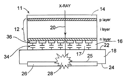
Fig. 3 illustrates a preferred embodiment of a flat panel detector 11 of the
present invention based on a direct multilayer selenium converter 12, under a
common conducting electrode 14. The converter 12 is positioned on a TFT array
16
which is placed on a glass substrate 18, the front side 22 of which is
connected to the
TFT array 16 and the rear side 24 is connected to a luminophor layer 26.
The multilayer selenium converter 12 successively incorporates under the
common electrode 14, a thin (2 to 3 pm) layer p made of doped selenium
material,
followed by a thick ( 1000 pm) layer of selenium alloy, followed by another
thin ( 1
pm) layer n of doped selenium. The materials and thicknesses of this pin
structure
given above are given by way of example and are not limitative.
The luminophor 26 provided on the rear side 24 of the glass substrate 18 is
adapted to stop the residual transmitted X-ray radiation. In Fig. 3, such
radiation
proceeds as shown by arrow 20 and is stopped by the luminophor 26 as
illustrated by
the burst of light 28. Preferably, such luminophor has an emission spectrum
within
the wavelength range of 580 nm to 620 nm. There is a choice of materials that
may be
used to produce such luminophor, for example having the following chemical
formulae: Zn3(P04)2; (Zn, Cd) S:Ag; YV04:Eu; Y203:Eu; Y202S:Eu and YZW30,Z:Eu.
The Eu doping with its Eu3+ ion has a 611 nm wavelength emission which
favorably
fits this wavelength range.
A further aspect of the present invention is to combine within the luminophor
26 two materials, one of which is used for X-ray absorption and the other for
light
emission at the proper wavelength. Thus, one can use, for instance, a
combination of
-9-
CA 02363663 2001-11-22
gadolinium oxisulfide and yttrium oxisulfide (Eu), the former essentially for
its high
X-ray stopping power, the latter for its appropriate spectrum emission. These
materials are currently used in X-ray film industry and the technology is thus
available in thick layers. A 300 mg/cm2 screen with 60% GdzO2S and 40% YZOzS
in
mole units, in an organic material binder and laminated in a sheet structure,
can
simply be coupled to the rear side 24 of the transparent glass substrate 18 of
the
detector 11 to form such luminophor combination designated as 26 in Fig. 3.
Considering an X-ray transmission of 30%, a light transmission through the
TFT structure of 30%, a luminophor yield of 5% in watts per watt, a light
collection
efficiency of 20%, at 1mR per frame and 30 frames per second, 1.66 E10 light
photons per second-cm2 will be absorbed in the selenium multilayer as a result
of the
back panel luminophor activation. The trapped charges to neutralize are a
function of
the irradiation and typically equal to about 0.01% of a steady X-ray signal.
After one
second irradiation at 1 mR per frame and 30 frames per second, the number of
charges trapped in deep sites seen through 1 cm2 of detector is in the lE7
range. The
light flux of some 1-E10 delivered by the back detector luminophor is thus
sufficient
to release the trapped charges.
Since an excess of light can create a background signal, the light flux on the
converter may be adjusted in order to deliver a neutralizing light flux
sufficient to
cancel any ghosting effect, but low enough to avoid any background or pedestal
signal. According to another aspect of the invention, this can be obtained by
interposing a light absorber between the luminophor 26 and the converter 12 or
by
adding a light absorber within the luminophor 26.
The light absorber interposed can be a semitransparent film of metal made of
-10-
CA 02363663 2001-11-22
titanium, chromium, gold or aluminum, deposited on the rear of the glass
support,
shown by line 25. If the luminophor is encapsulated in a binder, the latter
can be
tinted with a colored organic component. It can also contain a light absorbing
powder.
When combining an X-ray absorber with the luminophor, one can also adjust the
mixture in order to control the light flux to the fraction of the signal
corresponding to
the trapped charges.
The TFT array 16, built on a 1.1 mm thick glass substrate 18, typically has a
pitch of 150 pm. It has an array of storage capacitors 34 connected to
switches 36, as
shown schematically in Fig. 3.
The TFT matrix structure 30 is illustrated in Fig. 4 and its positioning
within
the detector structure is shown in Fig. 5. Each pixel 32 contains a storage
capacitance
34 and a TFT switch 36 with its source 37 connected to the upper capacitance
electrode 38, its gate 40 to common gate lines 42 which are common line scan
leads,
and its drain 44 to common drain lines 46 which are common column readout
leads.
The bottom electrode 48 of the capacitance 34, preferably made of ITO, is
deposited
on the glass substrate 18. Alternatively, this electrode 48 can be of the same
material
as the scan leads, namely chromium, titanium, molybdenum, aluminum or an
association of these metals. The upper electrodes 38 of the storage capacitors
34 a.re
in contact with charge collecting transparent conductive pads SO (preferably
made of
ITO) by vias 52, through transparent insulator material 51 which encapsulates
the
TFT array. The amorphous silicon TFT switch 36 covers a small portion of the
pixel
area, typically of the order of 20 x 20 ~m2, which only slightly obstructs the
transmission of light. Its gate insulator uses silicon nitride, silicon oxide
or organic
materials. The upper electrode 38 of the storage capacitance 34 is preferably
made of
-11-
CA 02363663 2001-11-22
transparent ITO. Alternatively it can also use chromium, titanium, molybdenum,
aluminum or an association of these metals. If the pixel electrodes are made
of
metallic material, the voids separating them from the scan and readout leads
will
insure the transmission of light from the underlying luminophor.
It should be noted that the invention is not limited to the preferred
embodiments described above, but various modifications obvious to those
skilled in
the art can be made without departing from the invention and the scope of the
following claims.
-12-