Note: Descriptions are shown in the official language in which they were submitted.
CA 02363830 2001-11-23
-1-
OPTICAL COUPLING DEVICE WITH ANISOTROPIC LIGHT-GUIDING
MEMBER
The present invention relates to an optical coupling device with an
anisotropic light-guiding member and, more particularly, to an optical
coupling device using a photonic crystal that propagates light with low loss
only in a particular direction.
In the field of optics various optical elements are used effectively for
particular purposes according to their physical properties as listed below.
Glass: Transmits light with low loss.
Lens: Converges diffused light and achieves a high coupling
effciency, or diffuses incident light.
Fiber optic plate: Formed by a fiber matrix of a reduced diameter of
several micrometers produced by drawing a bundle of optical fibers and
slicing it at right angles to its lengthwise direction. This plate guides
light
only in the direction at right angles to the plate, that is, has an
anisotropic
light guiding property.
Optical waveguide: Formed by surrounding a light propagation path of
a high refractive index material with a low refractive index material. This
optical waveguide confines therein light and guides it in a particular
direction.
Referring first to Fig. 1, a prior art example will be described below.
A glass block with parallel planes of incidence and emittance transmits
therethrough light incident on one of its end faces with a relatively low loss
and emits or radiates it from the other end face, but has no directionality in
its
propagation characteristic because of its isotropy. When a light beam LB
radiating from a single-mode optical fiber 10 with a divergence angle is
CA 02363830 2001-11-23
-2-
incident on the one end face 3F 1 of a glass block 3, the light beam LB
propagates in the glass block 3 while diverging and reaches the other end face
3F2 of the glass block 3 with the enlarged beam diameter. That is, even if
light of a small beam cross section is incident on the one end face 3F 1 of
the
glass block 3, it reaches the other end face 3F2 with an increased beam cross
section when the incident light has a divergence angle; consequently, the
light
coupling efficiency between the single-mode optical fiber 10 and a light
receiving element positioned on the other end face 3F2 is impaired by the
increased beam cross section. After all, it can be said that the glass block
has limited suitability as a material for optical coupling between optical
elements.
Fig. 2 depicts another prior art example. A lens 4 is capable of
converging a light beam, and hence it achieves a high coupling efficiency.
That is, the light beam LB radiated from the end face of the single-mode
optical fiber 10 with a divergence angle and impinging on the lens 4 while
diverging from its one focal point fl is refracted for convergence to the
other
focal point fZ. Accordingly, placement of the light receiving element 2 at
the position of the other focal point f2 of the lens 4 will provide a high
optical
coupling efficiency between the single-mode optical fiber 10 and the light
receiving element 2. In this instance, the attainment of increased optical
coupling efficiency calls for accurate alignment of the light receiving
element
2 with the focal point f2 of the lens 4. Since defocusing, even if it is
slight,
causes a serious reduction in the optical coupling efficiency, much difficulty
is encountered in the alignment of the light receiving element 2 with the
focal
point f2 for accurate focusing.
Fig. 3 shows still another prior art example. There is now placed on
the market a fiber optic plate 5 produced by fusing and drawing a bundle of
CA 02363830 2001-11-23
-3-
optical fibers with their gaps filled with a light absorbing material and
cutting
the optical fiber assembly to a desired thickness at right angles to its
lengthwise direction. The fiber optic plate 5 has a property of guiding light
lengthwise of optical fibers 51 forming the plate 5. That is, the light beam
LB incident to the one end face SF 1 of the fiber optic plate 5 propagates
therein only lengthwise thereof and reaches a light emitting end face SF2,
while light components diffusing in other directions than the lengthwise
direction of the optical fibers 51 are absorbed by the light absorbing
material
filling the gaps between them and hence do not reach the light emitting end
face SF2. Accordingly, the fiber optic plate 5 does not involve the use of a
lens for optical coupling between optical elements, and hence it eliminates
the
inconvenience of making adjustment for accurate focusing.
However, the fiber optic plate 5 allows leaky propagation or diffusion
of light in the other directions than in the lengthwise direction of each
optical
fiber 51 but absorbs such leaky components of light by the light absorbing
material interposed between the optical fibers 51 to thereby provide the
anisotropic light guiding property; therefore, the fiber optic plate 5
inherently
has the defect of high propagation loss. Further, the pitch of the fiber
matrix
of the commercially available fiber optic plate is also as large as several
micrometers, and consequently, in the case of optical coupling between it and
a single-mode optical fiber whose mode filed diameter (the emitted light
beam diameter) is as small as 9.5 pm, the number of fibers of the plate 5 that
are irradiated with the light beam emitted from the single-mode optical fiber
is only three to five. Hence, when the position of incidence of the light
beam from the single-mode optical fiber on the fiber optic plate 5 is shifted
relatively to each other, the quantity of light emitted from the fiber optic
plate
5 greatly changes in terms of the pitch of the fiber matrix. That is, to
CA 02363830 2001-11-23
-4-
improve the optical coupling efficiency calls for positioning of the fiber
optic
plate and the single-mode optical fiber relative to each other. For this
reason,
the fiber optic plate is not suited for use with the single-mode optical
fiber.
The afore-mentioned optical waveguide, though not shown, is able to
of guide light in an S-shaped path as well as in a straight line, and it is
also
capable of branching light into Y-cut paths. As is the case with the lens,
however, when the optical waveguide is used to couple optical elements, the
coupling efficiency decreases unless light is incident on the light
propagation
path at a proper position; hence, assembling of the optical waveguide with the
optical elements is time-consuming.
It is therefore an object of the present invention to provide an optical
coupling device with an anisotropic light-guiding component that is free from
the above-mentioned problems of the prior art.
The optical coupling device according to the present invention
comprises:
at least two optical elements; and
an anisotropic light-guiding member formed by a periodic two- or
three-dimensional arrangement of two or more kinds of dielectric materials of
different dielectric constants to develop a photonic band gap to inhibit the
propagation of light in directions except a particular one, the anisotropic
light
guiding member being disposed between the at least two optical elements.
In the above optical coupling device, at least one of the two optical
elements may be, for example, a single-mode optical fiber, laser diode, or
light receiving element.
The dielectric materials of the anisotropic light-guiding member may
CA 02363830 2001-11-23
-5-
be submicron in size and in the pitch of their periodic arrangement.
Further, the anisotropic light guiding member may be formed by
periodically arranging a particular kind of dielectric material molded in
spherical, columnar, prismatic or thin film form and filling their gaps with a
different kind of dielectric material.
Fig. 1 is a diagram explanatory of an optical coupling scheme using a
glass block;
Fig. 2 is a diagram explanatory of an optical coupling scheme using a
lens;
Fig. 3 is a diagram explanatory of an optical coupling scheme using a
fiber optic plate;
Fig. 4 is a diagram showing a three-dimensional photonic crystal;
Fig. 5 is a diagram showing a two-dimensional photonic crystal;
Fig. 6 is a diagram showing a homogeneous body;
Fig. 7 is a graph showing the energy level of the homogeneous body;
Fig. 8 is a graph explanatory of a photonic band gap;
Fig. 9 is diagram explanatory of an embodiment of the present
invention;
Fig. 10 is diagram explanatory of another embodiment of the present
invention; and
Fig. 11 is diagram explanatory of still another embodiment of the
present invention.
Fig. 4 is a diagrammatic representation of a photonic crystal 20
CA 02363830 2001-11-23
-6-
consisting of media of different dielectric constants E1 and s2 alternately
arranged in a three-dimensional periodic pattern. Fig. 5 is a diagrammatic
representation of a photonic crystal 20 consisting of media of different
dielectric constants E1 and s2 alternately arranged in a two-dimensional
periodic pattern.
The photonic crystals mentioned above are artificial crystal structures
in which two kinds of transparent media of widely different refractive indices
or dielectric constants are systematically arranged at intervals of the light
wavelength or at shorter intervals in an alternately repeating pattern. The
photonic crystals could be obtained by alternately arranging two kinds of
transparent media of the dielectric constants sl and s2 at intervals of
hundreds
to one-thousand-and-hundreds of nanometers. In such photonic crystals,
light in a particular frequency range will not propagate in any direction.
This frequency range is called a photonic band gap. The photonic crystal in
the narrow sense is a crystal in which no light in a particular frequency
range
will propagate in any three-dimensional directions, that is, no light exists.
In
general, however, photonic crystals include those in which no light propagates
only in particular directions. The tow- and three-dimensional photonic
crystals are already developed and manufactured (see Nikkei Electronics, No.
730, p.57-63, September 16, 1998 and Japanese Patent Application Laid-
Open Gazette 2000-258645).
Fig. 6 shows a homogeneous medium object of the dielectric constant
s2, whose energy level is continuous with respect to wave vector as depicted
in Fig. 7. On the other hand, the energy levels of the photonic crystals
formed by alternately arranging media of different dielectric constants E~ and
s2 in a periodic repeating pattern, shown in Figs. 4 and 5, are not continuous
with respect to wave vector. In particular, in a photonic crystal in which the
CA 02363830 2001-11-23
-7-
sizes of the media of the dielectric constants s~ and s2 and the pitch of
their
alternate arrangement are set to 1/2 of the optical wavelength, the
noncontinuity is large as depicted in Fig. 8. This noncontinuity, that is, the
gap, is called a photonic band gap (PBG), which is a forbidden band where no
light is allowed to exist theoretically as referred to above.
Let it be assumed that the photonic crystals 20 shown in Figs. 4 and 5
are perfect photonic crystals. By manipulating such a dielectric-constant
periodic structure, it is possible to fabricate a two- or three-dimensional
photonic crystal that has a continuous energy level only in a particular
direction and forms photonic band gaps in any other directions to inhibit
light
propagation. Such a two- or three-dimensional photonic crystal could be
implemented by removing part of the dielectric-constant periodic structure
from one side of the crystal to the opposite side in a straight-line direction
to
form a waveguide that permits light propagation only in that straight-line
direction. The light propagation loss is virtually zero in this waveguide.
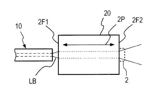
Next, a description will be given, with reference to Fig. 9, of an
optical multiplexer with an anitsotropic light guiding member according to an
embodiment of the present invention. The two- or three-dimensional
anisotropic light guiding photonic crystal 20 has a waveguide 2 formed by
removing its dielectric-constant periodic structure only in one straight-line
direction. In this embodiment the light receiving element 2 is mounted on
the light emitting end face 2F2 of the photonic crystal 20 on the side
opposite
the single-mode optical fiber 10. In Fig. 9 the light receiving element 2 is
indicated by the broken line with a view to showing the divergence of light
emitted from the light emitting end face 2F2.
The photonic crystal 20 transmits, in one direction, the light beam LB
incident to its one end face 2F 1 via the single-mode optical fiber 10 to the
CA 02363830 2001-11-23
- -
other end face 2F2 without diffusion during transmission. That is, the light
beam incident to the end face 2F 1 of the photonic crystal 20 propagates
therein with substantially no diffusion and hence with an extremely low loss,
and it is emitted from the end face 2F2 as a light beam of the same shape as
that of the incident light beam LB on the end face 2F1. This produces the
same effect as if the photonic crystal 20 does not exist as a propagation
medium, that is, as if the light emitting end of the optical fiber 10 is
present
on the light emitting end face 2F2, thereby achieving a high optical coupling
efficiency between the optical fiber 10 and the light receiving element 2.
Fig. 10 illustrates an embodiment of an optical package that is an
optical device with an anisotropic light guiding member. In this case, too,
the photonic crystal is the same as that used in Fig. 9. In Fig. 10, reference
numeral 20 denotes an anisotropic light guiding window member embedded
in one sidewall of a case 61 of an optical package 60, and 62 its lid. In the
case 61 a laser diode 7 for emitting light beam is mounted on the inner
vertical face 2F 1 of the anisotropic light guiding window member 20. The
single-mode optical fiber 10 is disposed with its one end face opposed to the
outer vertical face 2F2 of the anisotropic light guiding window member 20.
In this instance, since the light propagation characteristic in the
direction perpendicular to the vertical light-incidence face 2F 1 of the
anisotropic light guiding window member 20 is the same at any position on
the face 2F l, there is no need for making adjustments for relative
positioning
between the laser diode 7 and the anisotropic light guiding window member
20 and between the anisotropic light guiding window member 20 and the light
receiving end face of the single-mode optical fiber 10. That is, wherever the
laser diode 7 is placed on the inner vertical face 2F1, light incident thereto
propagates in the anisotropic light guiding member 20 in one direction while
CA 02363830 2001-11-23
-9-
keeping the shape of the light beam on the light-incidence face 2F 1 and
reaches the light emitting end face 2F2.
Accordingly, by adjusting the position of the end face of the single-
mode optical fiber 10 according to the point of arrival of light on the outer
vertical face 2F2 of the anisotropic light guiding window member 20, the
laser diode 7 and the light receiving end face of the single-mode optical
fiber
are brought into alignment with each other. Accordingly, the laser diode
7 and the single-mode optical fiber 10 can be centered simply by adjusting
their positions relative to each other without the need for taking into
account
10 the presence of the anisotropic light guiding window member 20.
Fig. 11 illustrates an example in which the optical coupler of the
present invention is applied to an optical connector. This example also uses,
as the anisotropic light guiding member, the photonic crystal 20 used in the
Fig. 9 example. In Fig. 11, reference numeral 11 denotes a first multi-
conductor single-mode optical fiber, 12 a first ferrule for holding one end
portion of the mufti-conductor single-mode optical fiber 11 in position, 21 a
second mufti-conductor single-mode optical fiber having its tip end face
coated with a filtering film, 22 a second ferrule for holding one end portion
of
the mufti-conductor single-mode optical fiber 21 in position, 20 an
anisotropic
light guiding member mounted on one end face of the second ferrule 21, and
27 a sleeve. The first and second ferrules 13 and 22 are fitted or inserted
into the sleeve 27 so that they are positioned relative to each other and
optically coupled.
Let it be assumed that the filtering film coated all over the end face of
the second mufti-conductor single-mode optical fiber 21 cuts off and reflects
light of a 1.31 ~,m wavelength but permits the passage therethrough of light
of
a 1.55 ~,m wavelength. With the first and second ferrules 12 and 22 coupled
CA 02363830 2001-11-23
-10-
together by the connector, when signal light having the 1.31 pm and 1.55 ~m
wavelengths multiplexed is input from the first mufti-conductor single-mode
optical fiber 11 via the anisotropic light guiding member 20, the filter
formed
over the entire area of the end face of the second mufti-conductor single-mode
optical fiber 21 inhibits the passage therethrough of the light of the 1.31
~,m
but permits the passage therethrough of the light of the 1.55 p,m wavelength
for input into the second mufti-conductor single-mode optical fiber 21.
At present, there is widely used an optical connector of the type that a
filter for cutting off light of a particular wavelength is directly formed on
one
end face of a mufti-conductor single-mode optical fiber. In the optical
connector two mufti-conductor single-mode optical fibers are repeatedly
connected to and disconnected from each other, the repeated direct
engagement of their end faces readily causes falling-off of the filter.
According to the present invention, the anisotropic light guiding
member 20 formed of a photonic crystal is pasted on the second ferrule 22
that is one end face of the optical fiber 22, and that end portion of the
optical
fiber having the filter formed on its end face is inserted and fixed in the
second ferrule 22. Accordingly, even if the first and second ferrules 12 and
22 are inserted into the sleeve 27 for abutment with each other, there is no
fear of the filter falling off since it is protected by anisotropic light
guiding
member 20 and the second ferrule 22. And, since the anisotropic light
guiding member 20 is interposed between the end face of the first multi-
conductor single-mod optical fiber 1 l and the filter-coated end face of the
second mufti-conductor single-mode optical fiber 21, it is possible to achieve
optical coupling between the optical fibers 1 l and 21 with a minimum of
crosstalk between them.
CA 02363830 2001-11-23
-11-
EFFECT OF THE INVENTION
As described above, the present invention uses, as the anisotropic light
guiding member, a two- or three-dimensional photonic crystal formed by an
arrangement of dielectric media that has a continuous energy level only in a
particular direction and forms the photonic band gap in any other direction to
inhibit light propagation; hence, the invention permits implementation of an
optical coupler that achieves low-loss optical coupling between various
optical elements as if no transmission medium exists.
15
25