Note: Descriptions are shown in the official language in which they were submitted.
CA 02363927 2001-11-27
SYNCHRONIZATION SIGNAL DETECTOR AND METHOD
FIELD OF THE INVENTION
This invention relates to a receiver detecting a synchronization (sync) signal
or
pattern sent by a transmitter to the receiver.
BACKGROUND OF THE INVENTION
In some communication systems, a data pattern or portion of a received signal
(i.e. a synchronization signal) is used to control decoding or other
processing of the
remainder of the received signal. In such systems, successful decoding or
processing
of a received signal is dependent upon accurate reception of the
synchronization signal.
The present invention addresses this need.
SUMMARY
According to an aspect of the invention, a sync signal detector comprises a
sync
signal generator for generating a reference sync signal, a sampler connected
to the
sync signal generator, a waveform correlator connected to the sampler, the
waveform
correlator receiving a input signal, and a peak detector connected to the
waveform
correlator and the sampler.
In a related embodiment of the invention, a process for detecting a sync
signal
within an input signal comprises the steps of: a) generating a version of the
sync signal,
b) correlating the sync signal with the input signal to generate a correlation
signal, c)
CA 02363927 2001-11-27
detecting a correlation peak in the correlation signal, d) estimating a timing
offset based
on the correlation peak for use by step a), e) repeating step a) to generate a
shifted
version of the sync signal using the timing offset estimated in step d), and
f) further
processing the input signal based on the shifted version of the sync signal
until the end
of the input signal.
A sync signal detector according to a further aspect of the invention
comprises
means for generating an internal sync signal, means for sampling said internal
sync
signal, the means for sampling operatively connected to the means for
generating,
means for correlating a waveform, the means for correlating operatively
connected to
the means for sampling, the means for correlating receiving a input signal,
and means
for detecting a peak, the means for detecting a peak operatively connected to
the
means for correlating and the means for sampling.
In accordance with another aspect of the invention, a method for detecting a
data pattern in an input signal comprises the steps of matching the data
pattern to a
known sync pattern using waveform correlation, shifting the known sync pattern
by a
timing offset determined from the waveform correlation to create a shifted
sync pattern,
and utilizing the shifted sync pattern to further process the input signal.
A still further embodiment of the invention comprises a computer readable
medium containing instructions for implementing a method for detecting a data
pattern
in an input signal, the method comprising the steps of matching the data
pattern to a
known sync pattern using waveform correlation, shifting the known sync pattern
by a
timing offset determined from the waveform correlation to create a shifted
sync pattern;
and utilizing the shifted sync pattern to further process the input signal.
-2-
CA 02363927 2003-09-05
According to an additional aspect of the invention, a wireless communication
device comprises a transceiver configured to transmit and receive
communication
signals, and a digital signal processor (DSP) operatively coupled to the
transceiver,
the DSP comprising computer software code for detecting a data pattern in a
communication signal, by performing the functions of matching the data pattern
to a
known sync pattern using waveform correlation, shifting the known sync patter
by a
timing offset determined from the waveform correlation to create a shifted
sync
pattern, and utilizing the shifted sync pattern to further process the
communication
signal.
According to another aspect of the invention, there is provided a
synchronization (sync) signal detector for detecting synchronization signals
in an
input signal, comprising a sync signal generator for generating a reference
sync
signal; a sampler coupled to the sync signal generator for sampling the
reference
sync signal; a waveform correlator coupled to the input signal and the sampled
reference sync signal for generating a correlation waveform; a timing offset
generator for receiving the correlation waveform and for generating a timing
offset
value that is used to time shift the reference sync signal; and a
synchronization
information calculator for receiving the time shifted reference sync signal
and the
input signal and for detecting whether a valid sync signal is present in the
input
signal.
In another aspect, there is provided a process for detecting a synchronization
(sync) signal within an input signal, comprising the steps of a) generating a
reference
sync signal; b) correlating the reference> sync signal with the input signal
to generate
a correlation signal; c) detecting a correlation peak in the correlation
signal; d)
estimating a timing offset based on the correlation peak for use by step a);
e)
repeating step a) to generate a time shifted version of the reference sync
signal
using the timing offset estimated in step d); and f) processing the input
signal and the
time shifted reference sync signal in order to detect whether a valid sync
signal is
present in the input signal.
In yet another aspect, there is provided a synchronization (sync) signal
detector, comprising means for generating an internal sync signal; means for
sampling the internal sync signal; means for correlating a waveform coupled to
the
sampled internal sync signal and are input signal and for generating a
correlation
waveform; means for detecting a ,»ak in the correlation waveform and for
CA 02363927 2003-09-05
generating a timing offset value that is used to time shift the internal sync
signal; and
means for detecting a valid sync signal by comparing the input signal to the
time
shifted internal sync signal.
In a further aspect, there is provided a method for detecting a data pattern
in
an input signal, the method comprising the steps of a) matching the data
pattern to a
known sync pattern using waveform correlation; b) shifting the known sync
pattern
by a timing offset determined from the waveform correlation to create a
shifted sync
pattern; and c) processing the input signal utilizing the shifted sync pattern
in order to
detect a valid data pattern in the input signal.
In another aspect, there is provided computer readable medium containing
computer executable instructions for implementing a method for detecting a
data
pattern in an input signal, the method comprising the steps of matching the
data
pattern to a known sync pattern using waveform correlation; shifting the known
sync
pattern by a timing offset determined from the waveform correlation to create
a
shifted sync pattern; and processing the input signal utilizing the shifted
sync pattern
in order to detect a valid data pattern in the input signal.
In yet a further aspect of the invention, there is provided a wireless
communication device, comprising a transceiver configured to transmit and
receive
communication signals; and a digital signal processor (DSP) operatively
coupled to
the transceiver, wherein the DSP detects a data pattern in a communication
signal
by performing the functions of a) matching the data pattern to a known sync
pattern
using waveform correlation; b) shifting the known sync pattern by a timing
offset
determined from the waveform correlation to create a shifted sync pattern; and
c)
processing the input signal utilizing the shifted sync pattern in order to
detect a valid
data pattern in the input signal.
BRIEF DESCRIPTION OF THE DRAWINGS
For a better understanding of the present invention, and to show more clearly
how it can be carried into effect, reference will now be made, by way of
example
only, to the accompanying drawings in which:
Figure 1 is a block diagram of a frame;
Figure 2 is a block diagram of a first communication signal receiver;
Figure 3 is a signal diagram illustrating waveform correlation;
Figure 4 is a signal diagram illustrating timing offset and waveform
correlation;
-3a-
CA 02363927 2003-09-05
Figure 5 is a graph indicating the effect of timing offset;
Figure 6 is a graphical representation of a time shift of a received signal;
Figure 7 is a graphical representation of a time shift of a sync signal;
Figure 8 is a block diagram of a sync signal detector in accordance with a
first
embodiment of the present invention;
-3b-
CA 02363927 2001-11-27
Figure 9 is a logical flow diagram of the process of the sync signal detector
of
Figure 8;
Figure 10 is a block diagram of a sync signal detector in accordance with a
second embodiment of the present invention;
Figure 11 is a logical flow diagram of the process of the sync signal detector
of
Figure 10;
Figure 12 is a block diagram of a second communication signal receiver; and
Figure 13 is a block diagram of a receiver incorporating a sync signal
detector
according to the present invention.
DETAILED DESCRIPTION OF THE INVENTION
In communications networks, such as a radio frequency (RF) communication
network, reception quality is improved if a receiver is able to synchronize
with a
transmitter. This synchronization aids the receiver in accurately receiving
and
processing the information provided by the transmitter.
Some known communication networks make use of packet based
communications. In such networks, a transmitter sends a stream of packets that
contain information to one or more receivers. Packets are often grouped
together to
form frames. Referring now to Figure 1, a block diagram of such a frame is
shown
generally as 10. As one skilled the art will appreciate, the structure of a
frame may vary
considerably and that frame 10 is only one example of a frame structure.
-4-
CA 02363927 2001-11-27
As illustrated in Figure 1, frame 10 comprises a frame head 12 and frame data
14. Frame head 12 contains information that provides a description of the
contents of
frame 10. Frame data 14 contains the packets.
Frame head 12 comprises: carrier portion 16, bit or symbol synchronization
pattern 18 (BS or SS), frame synchronization (FS) pattern 20, and other frame
head
information 22. The MobitexT"" wireless communication system uses frames of a
general structure similar to frame 10.
In the example frame head 12, the carrier portion 16 is an unmodulated signal
representative of the carrier used in the communication system over which
frames such
as 10 are transmitted and received, and allows a receiver to determine carrier
frequency. Bit sync pattern 18 is normally a known alternating pattern that
allows a
receiver to determine bit or symbol timing. Frame sync pattern 20 is a pattern
different
from bit sync pattern 18. Frame sync pattern 20 provides a different known
data or bit
pattern that will ideally only appear in a data stream or transmitted signal
when a frame
sync pattern 20 is actually being transmitted. Frame sync pattern 20 provides
synchronization information to a receiver. Other frame head information 22
includes
identification (ID) and control information, which may for example designate a
particular
decoding process to be used in a receiver. Thus, frame head 12 contains
information
required for successful reception of a transmitted frame by a receiver.
Referring now Figure 2, a block diagram of a first communication signal
receiver
is shown generally as 30. Receiver 30 comprises a receiver element 32, a
receiver
front end 34, a sync detector 36 and a receiver processing module 38. A signal
received at receiver element 32, which may for example be an antenna 32a or
wired
-5-
CA 02363927 2001-11-27
connection 32b, is processed by receiver front end 34, which may include such
functions as amplification, filtering and analog to digital conversion. Sync
detector 36
operates to detect synchronization signals such as the bit sync pattern 18 and
frame
sync pattern 20 in a received signal, as discussed further below, and may
provide sync
and control signals to receiver front end 34 and receiver processing module
38. Module
38 may for example include symbol detection, deinterleaving, decoding, error
detection,
error correction and other such signal processing functions. In many modern
receivers,
sync detector 36 and receiver processing module 38 would be implemented as a
digital
signal processor (DSP).
In known receivers such as the example receiver 30, the sync and control
signals
output from sync detector 36 would be used in other receiver components or
modules
to realign or shift a received signal to compensate for timing offset. As will
be apparent
to those skilled in the art, timing offset is the offset between actual sample
timing and
ideal sample timing, the ideal timing normally corresponding to sampling at
the centre of
a bit or symbol period. According to known techniques, when a sync signal or
pattern is
detected in a portion of a received signal, appropriate sync and control
signals are
output to other receiver components to effectively realign the received signal
and the
receiver sample timing such that the actual sample timing approaches the ideal
timing.
In conventional signal receivers, particularly in digital receivers operating
on
digitized versions of received signals, the received signal is stored and can
be
"replayed" and re-sampled to correct for timing offset. However, such re-
sampling of
the received signal tends to involve substantial processing, as the entire
received signal
must be replayed and re-sampled. In addition, it would be desirable to
determine the
-6-
CA 02363927 2001-11-27
modulation index, a measure of signal gain, and frequency offset of the
received signal
from a detected sync signal. Since a received sync signal should exhibit a
known
pattern, the modulation index and frequency offset can be accurately
determined by a
sync signal detector, provided that the sample timing of the received signal
and the
receiver are the same. To determine the modulation index and frequency offset
would
also require re-sampling of the received signal in prior art systems and is
therefore
similarly processing intensive.
Therefore, there remains a need for a less intensive sync signal detection
system and method that involves fewer signal processing functions and thereby
reduces the complexity of the sync signal detector and the time associated
with sync
signal detection operations. The present invention meets this need by using a
waveform correlation for sync signal detection and shifts a reference sync
signal
instead of the received signal to compensate for any timing offset.
As discussed above, the bit sync pattern 18 and frame sync pattern 20 are
known patterns which occur at known positions in a received frame 10 and can
therefore be used to synchronize a receiver 30.
Figure 3 is a signal diagram illustrating waveform correlation. In Figure 3,
an
example portion of a received frame head is shown as signal 40. Signal 40
comprises
bit sync pattern 18 and frame sync pattern 20. Carrier portion 16 and other
frame head
information 22 are neither directly involved in nor affected by the invention
and
therefore are not shown. The period of signal 40 is shown by feature 52, which
for the
purpose of this example is a one bit or symbol period. The particular patterns
shown in
_7_
CA 02363927 2001-11-27
Figure 3 are illustrative examples only. As one skilled in the art will
recognize the
invention is in no way restricted to the example signal shown.
A signal receiver 30 which receives a frame such as frame 10 would normally
initially detect carrier portion 16 and then establish bit or symbol timing
based on bit
sync pattern 18 to enable receiver 30 to detect bits or symbols. Having
established bit
or symbol timing, receiver 30 then begins detecting bits or symbols to search
for frame
sync pattern 20 on a bit-by-bit (bit correlation) or symbol-by-symbol (symbol
correlation)
basis. When the frame sync pattern 20 is detected, receiver 30 can determine
timing
offset, adjust sampling the incoming received signal accordingly and proceed
with
further processing of the received signal. In most conventional receivers, the
frame
sync pattern 20 is detected in a portion of the received signal when the
number of bits
or symbols that differ from frame sync pattern 20 is below a predetermined
threshold,
normally one or more bits or symbols.
Known synchronization processes operate effectively under good signal
conditions and may be sufficient for some applications. However, in many
communication environments, signal quality can potentially vary below levels
required
for reliable sync signal detection. For example, at low signal to noise ratios
(SNRs), the
duration of the carrier portion 16 and the bit sync pattern 18 tends to be too
short to
allow for accurate bit or symbol timing determination, such that the frame
sync pattern
20 cannot be detected and the received signal cannot be properly processed.
Synchronization signal detection can be improved by using waveform correlation
techniques as illustrated in Figure 3. Waveform correlation exploits the fact
that both
the relative location and the shape of sync signals will necessarily be known
to a
_g_
CA 02363927 2001-11-27
receiver 30. Instead of searching for sync signals on a bit-by-bit or symbol-
by-symbol
basis, a waveform correlator compares the entire known pattern or signal shape
to a
received signal and generates a corresponding metric indicating the similarity
of the
received signal to the known signal.
Waveform correlation essentially involves "sliding window" type processing.
Portions of the received signal, one of which is shown as window portion 40,
corresponding in length to the known sync signal 42, are compared to the known
sync
signal 42 in an attempt to achieve a matching signal 46. The sliding function
is
indicated by the arrow 44. The resulting calculated correlation or metric
values should
be relatively low for all window positions in the received signal except for
the matching
signal 46. The position of the peak 48 of correlation waveform 50 indicates
the
presence of the sync signal 42. Although the example in Figure 3 illustrates
correlation
of the bit sync pattern 18 and the frame sync pattern 20 to the received
signal, other
signal correlations, for example the correlation of either of the bit sync
pattern 18 or the
frame sync pattern 20 to the received signal, may also or instead be
performed.
Conceptually, the sync signal detection process is straightforward.
Correlation
peak 48 tends to be pronounced and should thus be relatively easily detected.
However, in digital receiver arrangements, waveform correlation operations are
performed on signal samples. Although detection of the highest correlation
waveform
sample remains simple, unless a sampling instant occurs at the peak 48 of the
waveform 50, then the peak sample is not the true peak of the correlation
waveform
and therefore does not accurately indicate the position of the sync signal 42.
As
discussed further below, the amplitude of the peak sample may also be
inaccurate.
_g_
CA 02363927 2001-11-27
Figure 4 is a signal diagram illustrating timing offset and waveform
correlation.
Figure 4 provides an example of the digital peak detection problem and its
cause in
digital receivers. In Figure 4, signal 60 represents a portion of a received
signal. Signal
62 is a portion of the known sync signal 42 to be detected. Signal 64
represents a
portion of the correlation waveform 50 comprised of correlation values or
metrics
generated by a waveform correlator. Bit or symbol periods are denoted by the
vertical
dashed lines having a period illustrated by feature 52 as in Figure 3. For the
purpose of
clarity, only a portion of the received signal, the known sync signal and the
correlation
waveform are shown in Figure 4. It will be apparent to those skilled in the
art that the
received signal samples would correspond to sampling at a sampling rate of at
least
twice the bit or symbol rate of the received signal. However, Figure 4 and
subsequent
Figures show only a single sample per bit or symbol period 52 in order to
avoid
congestion in the drawings.
Ideally, the received signal will be sampled at the centres of the bit or
symbol
periods 52. In practical systems however, there is often a timing offset
between actual
sampling instants and the bit or symbol period centres. The known sync signal
42
would be generated in a receiver and therefore its sampling can be controlled.
According to known techniques, the locally generated sync signal samples 66
are
representative of mid-period sampling. Although the received signal samples 68
are
offset from the sync signal samples 66 by timing offset 70, the correlation
waveform 64
will exhibit a relative peak when the known sync signal 62 has been aligned
with
window portion 60. The pattern of a sync signal 42, of which only a portion 62
is shown
in Figure 4, is normally chosen to ensure that no other expected signal
patterns will
-10-
CA 02363927 2001-11-27
approximate the pattern of sync signal 42 closely enough to incorrectly
indicate the
presence of sync signal 42. Therefore, alignment of a known sync signal 42
with a
portion of a received signal which contains the sync signal should always
result in a
correlation peak.
Detection of the peak sample 72 in the correlation waveform 64 is relatively
straightforward. In the presence of timing offset 70, however, peak sample 72
does not
correspond to the true correlation peak 74. Any estimate of sync signal
position or
amplitude based on peak sample 72 may therefore be in error. Samples before
and
after peak sample 72 are shown as features 76 and 78 respectively. Although
not
shown in Figure 4, at a sampling rate of twice the bit or symbol rate, peak
sample 72
may be offset from true correlation peak 74 by up to one-quarter of a bit or
symbol.
Ideally, the value of timing offset 70 should be zero, although in practical
systems,
offsets of up to about one-sixteenth of a bit or symbol are typically
acceptable.
Figure 5 is a graph indicating the effect of timing offset. As shown in the
Figure
5, estimated values along curve 80, which would be sample values in digital
receivers,
can vary with timing offset. These values may for example be such signal
characteristics as timing offset, frequency offset or modulation index. Within
the above
example range of 10.25 bits or symbols, estimates may vary up to a delta of
10%
(feature 82), which will be unacceptable in many applications, particularly
those in
which soft signal receiver processing is required or desired.
Using a correlation waveform such as 64, timing offset can be estimated by
using curve fitting techniques. In accordance with such techniques (e.g. least
squares),
a true correlation waveform peak, shown at 74 in Figure 4, is approximated by
a
-11-
CA 02363927 2001-11-27
parabola which is a best-fit to the peak sample 72 and two adjacent samples 76
and 78
(Figure 4). The position of the true correlation peak 74 can then be estimated
and
compared with the peak sample 72 to determine an estimate of the timing offset
70.
The timing offset estimate may then be fed back to the receiver front end 34,
fed
forward to the receiver processing module 38 or both, dependent upon the
particular
receiver architecture and synchronization arrangement of receiver 30 (Figure
2). In
known receivers, the timing offset estimate is used to determine a time shift
required to
compensate the received signal for the timing offset. The time shift may be
applied to a
received signal in digital receivers by "replaying" the received signal from
memory with a
delay or advance corresponding to the timing offset estimate and re-sampling
the
replayed signal. In many receivers the replaying and re-sampling functions
would be
performed by calculating new signal samples based on stored samples of a
received
signal.
Figure 6 is a graphical representation of a time shift of a received signal. A
time
shift 90 (based upon an estimate of timing offset 70) might be applied to a
portion of a
received signal 60 by replaying signal 60 to create new shifted signal 60a.
Shifted
signal 60a may then be re-sampled at the sampling instants, as shown. Other
techniques for applying a time shift 90 to a portion of a received signal 60
will also be
apparent to those skilled in the art, such as replaying the signal 60 from
memory and
adjusting sampling instants to compensate for estimated timing offset 70..
Such
techniques have been used in conjunction with known sync detectors to shift
signal 60
to compensate for timing offset 70.
-12-
CA 02363927 2001-11-27
Figure 7 is a graphical representation of a time shift of a sync signal.
Rather
than applying a time shift (based upon an estimate of timing offset 70) to a
portion of a
received signal 60, the present invention applies a time shift 94 to sync
signal 42 to
create new sync signal 42a. Instead of correcting for timing offset 70, which
is
essentially an error in the incoming signal, the present invention processes a
locally
generated reference sync signal 42 to effectively introduce a corresponding
amount of
error, contrary to the teachings of all known prior art. This results in the
creation of a
new reference sync signal 42a. As shown in Figure 7, the sync signal sampling
is
effectively time shifted by an amount corresponding to the estimated timing
offset 70.
Such time shifting of the sync signal sampling may be achieved by shifting
either the
locally generated reference sync signal 42 or the sample timing.
The time shifting of the locally generated reference sync signal 42 or its
sample
timing to create reference sync signal 42a improves the operation of a sync
signal
detector, since sample timing in a time shifted reference sync signal 42a is
the same as
or very close to sample timing in a received signal. Therefore, both the
amplitude and
location of samples in the reference sync signal accurately indicate the
amplitude and
position of the samples of a portion of the received signal that includes the
sync signal.
This improves both sync signal detection reliability and noise immunity and
also
provides for more accurate estimation of modulation index and frequency
offset, as
described in further detail below.
A further advantage of time shifting a reference sync signal 42 instead of the
received signal is that the known sync signal 42 is generated at the receiver.
As such,
a sync signal detector 36 (Figure 2) has full control of sync signal
generation and
-13-
CA 02363927 2001-11-27
sampling. Shifting of either the locally generated sync signal 42 or a timing
signal
controlling the sampling thereof is a more simply and easily implemented than
the
known received signal shifting techniques. In addition, sync signal 42 is
typically much
shorter than the entire received signal and therefore requires less processing
to re-
sample.
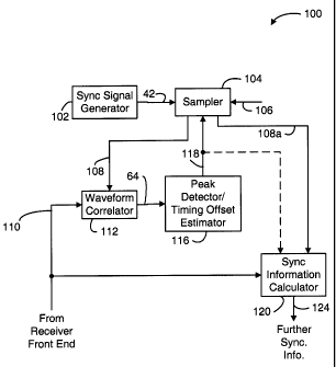
Referring now to Figure 8, a block diagram of a sync signal detector in
accordance with a first embodiment of the present invention is shown generally
as 100.
Detector 100 may be viewed as providing the functionality of block 36 of
Figure 2. A
sync signal generator 102 outputs the known sync signal 42 to be detected by
detector
100 to a sampler 104. Sampler 104 may for example be a sample and hold
circuit,
analog to digital converter (ADC) or the like. Sampler 104 samples or
digitizes sync
signal 42 in accordance with a sampling signal 106, which in most embodiments
would
be generated by a local oscillator or frequency synthesizer in a receiver, and
outputs
digitized reference sync signal 108. An input signal 110 from the receiver
front end 34
is correlated with reference sync signal 108 by waveform correlator 112. A
correlation
waveform 64 generated by correlator 112 is output to a peak detector and
timing offset
estimator 116. Estimator 116 operates as discussed herein above to estimate
timing
offset. Estimator 116 outputs a control signal 118 to either the sampler 104
as shown,
or alternatively to the sync signal generator 102, to effectively time shift
the sampling
instants or generated sync signal 42 according to the estimated timing offset.
In digital
receivers, the sync signal generator 102 and sampler 104 may be implemented as
a
single functional block in a DSP, such that digital sync signal sample values
are
calculated in accordance with the sampling signal 106 and control signal 118,
without
-14-
CA 02363927 2001-11-27
generating an analog sync signal 42. In the detector 100, the algorithm
utilized by sync
information calculator 120 may also be adjusted in response to timing offset
estimates
from estimator 116.
The time shifted version 108a of the reference sync signal is then input to
the
sync information calculator 120. The calculator 120 uses the shifted reference
sync
signal 108a and the received signal 110 to calculate further sync information
such as
modulation index and frequency offset, and may also make a final determination
of
whether or not a sync signal detected in a received signal is actually a valid
sync signal.
Calculator 120 may also receive the outputs from estimator 116 for calculation
of the
further sync information. The sync information determined by calculator 120 is
preferably provided to other components (not shown) of a receiver in which the
detector
100 is implemented, as signal 124.
Referring now to Figure 9, a logical flow diagram of the process of the sync
signal detector of Figure 8 is shown generally as 150. Process 150 begins at
step 154
when a signal 110 is received. Moving next to step 156 a timing offset value t
offset is
initialized, preferably to zero. Although an initial timing offset of zero is
preferred, other
initial offsets, such as a previous timing offset estimate, may also be used.
A digital
version of the known sync signal 42 is then generated. In the example frame
shown in
Figure 1, sync signal 42 preferably includes the bit sync pattern 18, the
frame sync
pattern 20, or both.
Sync signal 42 may be generated by first generating an analog version of the
sync signal with the timing offset of t offset and sampling the generated
signal, as
indicated at steps 160 and 162. Alternatively, an analog version of the known
sync
-15-
CA 02363927 2001-11-27
signal 42 may first be generated at a step 164 and sampled as at step 166,
with the
sample timing at step 166 being shifted relative to ideal mid-period sampling
by a timing
offset of t offset. In digital implementations, a digital version of the known
sync signal
42 corresponding to sampling with a timing offset of t offset could be
calculated directly
or generated from stored samples for example, at a step 168. A particular
implementation of the present invention would preferably use only one of these
sync
signal generation techniques.
Before sync signal 42 has been detected in a received signal 110, the timing
offset used for generation of sync signal is the initial value of t offset set
at step 156.
Those skilled in the art will appreciate that since the sync signal is a known
signal, the
sync signal generation steps shown in Figure 9 may be performed in parallel
with
receiver front-end processing which produces signal 110. Other relative
timings of
these operations are within the scope of the invention.
At step 174, it is then determined whether or not the generated reference sync
signal was generated using the initial offset established at step 156 or is a
shifted sync
signal generated using an offset estimated following a correlation operation.
The
determination at step 174 may be accomplished with a repeat count index,
initialized at
the beginning of the sync signal detection operations and incremented after
correlation
waveform peak detection and timing offset estimation. Such repeat count index
initialization and increment steps will be apparent to those skilled in the
art, but have not
been shown in Figure 9 in order to avoid congestion in the diagram. Other
techniques
may also be used to determine if the generated sync signal is an initial sync
signal or a
post-correlation shifted sync signal.
-16-
CA 02363927 2001-11-27
If a correlation has not yet been performed, then waveform correlation as
described above is performed at step 170, and continues until a correlation
peak is
detected. When a peak is detected at step 172, a new timing offset new t
offset is
estimated at step 176 and the timing offset value t offset is updated with the
new timing
offset estimate new t offset at step 178. For example, new t offset may be
calculated
as follows:
new _ t _ offset = Co - Cz
2*~Co _2*Ci _Cz)
where Co, C~ and C2 respectively correspond to correlation signal samples 76,
72, and 78 (see Fig. 4), that are output by the correlation block 170 in Fig.
9.
Process 150 then returns to step 160, 164, or 168, depending upon how the
known sync signal 42 is generated. The sync signal 42, time-shifted in
accordance with
the updated timing offset is then generated and a positive determination will
be made at
step 174. The shifted sync signal is then processed at step 180 to determine
other
synchronization information or parameters, such as modulation index and
frequency
offset for example. As described above, calculated sync information or
possibly other
signal parameters may be used to determine whether or not a sync signal
detected in a
received signal is valid, as shown at step 182. If the detected sync signal is
determined
to be valid, then any calculated sync information, and possibly the shifted
sync signal, is
output to further components of a receiver at step 184, and the sync signal
detection
process 150 ends at step 186. If the sync signal is not determined to be
valid, resulting
in a negative determination at step 182, then control returns to step 156,
where timing
-17-
CA 02363927 2001-11-27
offset is re-initialized at step 156 and process 150 is repeated using a
subsequent
portion of the received signal.
Those skilled in the art will appreciate that although the sync signal
detection
process 150 ends after a sync signal is determined to be valid, processing of
a received
signal by other receiver components based on a detected valid sync signal may
continue thereafter. The sync signal detection process 150 would then be
repeated
when a portion of a received signal, such as a complete frame for example, has
been
processed and a new sync signal must be detected.
Referring now to Figure 10, a block diagram of a sync signal detector in
accordance with a second embodiment of the present invention is shown
generally as
200. Sync signal detector 200 includes a phase calculator 202 and a frequency
modulation (FM) demodulator 204, in addition to a sync signal detection
arrangement
similar to the detector 100 of Figure 8. Detector 200 operates similarly to
detector 100
to perform a correlation in correlator 112, estimate timing offset in
detector/estimator
116, time shift the known sync signal 42 generated by generator 102 and
sampler 104
and provide the shifted sync signal 108a to the sync information calculator
120.
Detector 200 assumes that the received signal 110 is frequency modulated.
Therefore,
modules 112, 116 and 120 may differ slightly from the corresponding modules in
detector 100. However, the overall operation of the detectors 100 and 200 to
determine
timing offset and shift the locally generated sync signal is substantially the
same.
In detector 200, the sync information calculator 120 determines whether or not
a
valid sync signal was received, for example by calculating and comparing a
-18-
CA 02363927 2001-11-27
characteristic of the received signal to a certain threshold, and outputs
modulation
index (g) 206 and frequency offset (dc) 208 as described below.
The modulation index (g) 206 and frequency offset (dc) 208 may be estimated as
follows:
1
~r *t; --~ryt~
g = r N . . do = 1 r. ~t.
t2 - 1 t2 ~ N ~ ~ - gLr r
r i
N ;
where i = 1,2, .. . N are indexes of the received signal (r) and the reference
sync
signal (t) generated by the detector 200.
In a preferred embodiment of the invention, samples of a received signal
output
by the FM Demodulate block 204 are compared to the shifted sync signal, re-
sampled
at new t offset and adjusted by the modulation index (g) 206 and frequency
offset (dc)
208 to calculate the amount of noise E present in the portion of the received
signal in
which the sync signal was detected:
E = ~ ~r,. - gt; - dc~2 .
E is compared to a threshold T to determine whether or not the received signal
samples r; represent a valid sync signal. This particular example
implementation
calculates g and do followed by the calculation of E using previously
calculated values
(g and dc) involving the received signal samples r; and sync signal samples
t;.
Calculation of g and do may also be optimized by storage and re-use of sums of
received signal samples and sync signal samples. For example, sums of r; and
t; occur
_19_
CA 02363927 2001-11-27
in the above equations for both g and dc. Therefore, these sums need only be
calculated once, stored to a memory, and used to calculate both g and dc.
The above expressions for E, g and do are provided for illustrative purposes
only. The invention is in no way restricted thereto. Other sync information
and signal
characteristics may be calculated and used either by further receiver
components or to
determine whether or not a detected sync signal is valid.
The method of generating the sync signal (t) sampled at new t offset makes the
above calculation algorithm for modulation index and frequency offset
insensitive to
received signal sampling phase and thus eliminates the requirement to resample
and
re-demodulate received signal samples. It also allows for a fixed threshold T
to be
established for determination of the validity of a detected sync signal that
directly
relates to the probability of a missed sync signal detection event which was
not possible
according to prior art sync signal detection techniques.
In prior art sync signal detection systems, calculation of these or any other
parameters derived from the correlation waveform 64 is not feasible. As
described
above, prior art receivers typically replay and resample the received signal
110 instead
of the sync signal 42 with which the received signal 110 is correlated. Thus,
the
samples in a locally generated reference sync signal indicate the amplitude
and position
of the sync signal samples in the received signal, which provides for more
accurate
estimation of modulation index and frequency offset estimation.
The signals output from detector 200 are preferably input to other receiver
components. For example, modulation index 206 might be input to a receiver
gain
control stage. Frequency offset 208 may be connected to a frequency control
-20-
CA 02363927 2001-11-27
arrangement, a filter, a frequency converter or other receiver components that
perform
frequency related or frequency dependent functions. Modulation index 206 and
frequency offset 208 are but two parameters that may possibly be calculated
from the
correlation waveform 64 and received signal 110. Other sync parameters and
information could also or instead be calculated, depending upon the particular
receiver
in which the present invention is implemented.
Referring now to Figure 11, a logical flow diagram of the process of the sync
signal detector of Figure 10 is shown generally as 300. Since the second
embodiment
is substantially similar to the first embodiment, most of the process steps
shown in
Figure 11 are the same as those shown in Figure 9. As mentioned above however,
the
second embodiment assumes that the received signal 110 is frequency modulated.
Phase calculation step 302 and FM demodulation step 304, are therefore shown
in
Figure 11. The sync signal generation steps (160, 162, 164, 166, 168),
waveform
correlation step 170 and peak detection step 172 may also differ from
corresponding
steps in Figure 9 but, as discussed above, would perform similar functions.
The
operations performed by sync information calculator module 120 in Figure 10
are
shown in Figure 11 as steps 306 and 308. The steps in the second embodiment
are
otherwise the same as described above in relation to the first embodiment.
Having described illustrative embodiments of the invention, some examples of
contemplated implementations will now be described. Sync signal detectors and
methods according to the invention may for example be implemented in receivers
having a general structure as shown in Figure 2. Implementation of the present
-21-
CA 02363927 2001-11-27
invention in similar receivers as those having a general architecture as in
Figure 12 is
also contemplated.
Figure 12 is a block diagram of a second communication signal receiver shown
generally as 320. Figure 12 is similar to Figure 2, but illustrates an
alternate
arrangement of the receiver front end 34, sync signal detector 36 and receiver
processing module 38. In receiver 320 a signal receiving element 32, either an
antenna
32a for wireless communication systems or a wired connection 32b for wired
communication systems, inputs a received signal to receiver front end module
34. As
discussed above in reference to Figure 2, receiver front end module 34 may
perform
such functions as amplification, filtering and analog to digital conversion.
Receiver front
end module 34 then provides an input signal to processing module 38. Sync
signal
detector 36 operates in accordance with the invention to detect sync patterns
in the
received signal and apply a time shifting function to a locally generated sync
signal.
Receiver 320 differs from receiver 30 in that sync signal detector 36 is not
connected in
the signal path between the front end 34 and processing module 38. Receiver
processing module 38, may include symbol detection, deinterleaving, decoding,
error
detection, error correction and other such signal processing functions. In
preferred
embodiments of the invention, at least the sync signal detector 36 is
implemented with
digital components or in a DSP.
Figure 13 is a detailed block diagram of a receiver in which the invention may
be
implemented. The receiver 350 includes an antenna 32a, the output of which is
filtered
in a frequency band filter 352. Down converter stage 354 converts the filtered
signal
from the filter 352 from a higher frequency to a lower frequency, typically
from radio
-22-
CA 02363927 2001-11-27
frequency (RF) to intermediate frequency (IF). IF channel filter 356 is a band
pass filter
that filters the down converted signal to select a particular IF channel in
the down
converted signal. Receiver 350 also includes an adjustable gain stage 358,
which as
known in the art can be controlled by a gain control signal generated by other
receiver
components described below.
A quadrature mixer 362 separates the in-phase (I) and quadrature (Q)
components of the received signal. Low pass filters 364a and 364b filter out
image
signal components from the output of mixer 362 and limit the input bandwidth
sampled
by the ADCs 366a and 366b. The ADCs 366a and 366b provide for signal
processing
functions in the digital domain, which is preferred for the instant invention.
Digital outputs from the ADCs 366a and 366b are input to a digital signal
processor (DSP) 370. In the receiver 350, the I and Q components from ADCs
366a
and 366b are input to channel filter 372 in DSP 370. The output from filter
372 is input
to a frequency control unit 374, which generates a frequency control signal
which in turn
controls the local oscillator (LO) and frequency synthesizers generally
designated 376
in Fig. 14 and a gain control unit 378, which generates a gain control signal
for gain
stage 358. DSP 370 is a digital component, whereas gain stages and frequency
synthesizers normally use analog control signals. Digital to analog converters
(DACs)
380a and 380b may therefore also be provided in the receiver 350. As shown,
the LO
and frequency synthesizers module 376 provides frequency reference signals
frefl ,
fref2 and fref3 on its outputs 376a, 376b, and 376c. In the example receiver
350, these
reference signals are provided to the down converter 354, quadrature mixer 362
and
other receiver modules.
-23-
CA 02363927 2001-11-27
The output signal from channel filter 372 is also input to a re-sampler 382,
which
essentially realigns sample timings in accordance with synchronization
information
provided by frame sync detector 384. It should be noted that this re-sampling
is
performed by the re-sampler 382 is based on the accurate timing offset
estimate and
possibly further sync info from the frame sync detector 384, not as part of
the sync
signal detection as in known receivers. Frame sync detector 384 operates in
accordance with the frame sync detection techniques described above to detect
frame
sync patterns in received signals. As discussed above, frame sync detector 384
may
detect bit sync information as well, it is not restricted to simply
recognizing a "frame
sync" per se, but for simplicity we refer to it as a frame sync detector.
Frame sync detector 384 detects a unique pattern or signal that is
periodically
inserted in a transmitted signal to maintain synchronization between a
transmitter and
receiver. In the Mobitex wireless communication system for example, the
maximum
length of a transmitted frame is about 1 second, so a Mobitex receiver should
receive a
frame sync pattern at least once every second. Frame sync detector 384 outputs
synchronization information that may be used by other receiver components such
as
the symbol detector 386, the operation of which will be apparent to those
skilled in the
art, to maintain synchronization. As described above, a frame sync detector
384 in
accordance with the present invention provides for implementation of symbol
detector
386 as a soft decision symbol detector. Other receiver components that receive
sync
info from the detector 384 and/or received signal information from the symbol
detector
386 may include further DSP components, and/or components that are not
implemented as part of the DSP 370. Although these other receiver components
will
-24-
CA 02363927 2001-11-27
differ for different receivers, many receivers include components to perform
one or
more of the operations of descrambling, deinterleaving, decoding, decryption,
error
checking and error correction. In addition, a microprocessor or software
application in a
communication device in which the receiver 120 is implemented may process data
in a
received signal. If detector 384 is implemented as shown in Figure 10, the
phase
calculator 202 could be a rectangular to polar coordinate converter. Such a
converter
would convert the rectangular I and Q (I + jQ) signal components input to
detector 384
from the re-sampler 382 into polar amplitude and phase components (A L~ ), of
which
the phase ~ would be input to the FM demodulator 204. Frame sync detector 384
would then operate as discussed above to generate frequency offset and
modulation
index estimates, which may be fed back to frequency control unit 374, gain
control unit
378 or other receiver components.
Further synchronization and control parameters may also be calculated in frame
sync detector 384 for input to frequency control unit 374, gain control unit
378, re-
sampler 382, symbol detector 386, and any other receiver components as shown
in the
Figure 13. For example, for M-ary symbols, comprising M values per symbol, non-
linearity of a communication channel could be computed by the frame sync
detector
384 and provided to other receiver components.
Receiver 350 represents an illustrative embodiment of the present invention.
Practical implementation of the invention is not intended by the inventors to
be
restricted to the example of receiver 350. The present invention is applicable
to both
wired and wireless receivers, which may or may not include all of the
functional blocks
-25-
CA 02363927 2001-11-27
shown in Figure 13. Similarly, receivers or communication devices in which the
invention is implemented may also include further functions and components in
addition
to those disclosed above. In many contemplated embodiments, a receiver
embodying
sync pattern detection in accordance with the invention would be a part of a
two-way
communication device, which would also include a transmitter.
Although described primarily in the context of a particular receiver
architecture,
the invention may be applied to virtually any wireless communications device
in which
sync pattern detection is required. Wireless modems such as those disclosed in
United
States Patent 5,619,531, titled "Wireless Radio Modem with Minimal Interdevice
RF
Interference", issued on April 8, 1997, and United States Patent 5,764,693,
titled
"Wireless Radio Modem with Minimal Inter-Device RF Interference", issued on
June 9,
1998, both assigned to the assignee of the instant invention, represent types
of
communication devices in which the invention may be implemented. Many
conventional
wired modems also require sync pattern detection and therefore would be
suitable for
application of the invention.
In further preferred embodiments, the invention may be configured to operate
in
conjunction with mobile communication devices, such as those disclosed in co-
pending
United States Patent No. 6,278,442, issued on August 21, 2001, and entitled
"Hand-
Held Electronic Device With a Keyboard Optimized for Use With the Thumbs".
Other
systems and devices in which the invention may be implemented include, but are
not
limited to, further fixed or mobile communication systems, hand-held
communication
devices, personal digital assistants (PDAs) with communication functions,
cellular
telephones, one-way pagers and two-way pagers.
-26-
CA 02363927 2001-11-27
It will be appreciated that the above description relates to preferred
embodiments by way of example only. Many other variations of the invention
will be
obvious to those knowledgeable in the field, and such obvious variations are
within the
scope of the invention as described and claimed, whether or not expressly
described.
For example, the invention need not necessarily be part of a DSP and
implemented
primarily in software as in the above preferred embodiments. The sync signal
detection
techniques according to the invention may also be at least partially
implemented in
hardware. Further as one skilled in the art will recognize our use of the term
"frame
sync" applies to only one type of synchronization signal. The present
invention may be
used to detect any synchronization pattern.
_27_