Note: Descriptions are shown in the official language in which they were submitted.
CA 02363930 2001-11-27
SYSTEM AND METHOD FOR SYNCHRONIZATION SIGNAL DETECTION AND
RECOVERY FROM FALSE TRIGGERS
BACKGROUND OF THE INVENTION
Field of the Invention
This invention relates generally to communication signal receivers and in
particular to synchronization detection in signal receivers.
Description of the State of the Art
In some known communication systems, an initial data pattern or portion of a
received signal is used by receivers to control decoding or other processing
of the
remainder of the signal. Therefore, successful decoding or processing of a
signal is
dependent upon accurate reception of the initial data pattern.
This type of initial data pattern may be referred to generally as a
synchronization (sync) signal. In order to properly process a received signal,
the sync
signal must be received and decoded correctly. However, a sync signal
detection scheme
may from time to time erroneously detect a sync signal, resulting in increased
data
processing errors, since the erroneously detected sync signal is not a valid
sync signal.
Known receivers do not provide effective mechanisms for recovering from
erroneous sync
signal detections, commonly called false triggering.
Therefore, there remains a need for a system and method for detecting a
sync signal, which provide for reliable and effective recovery from false
triggering.
-1-
CA 02363930 2001-11-27
SUMMARY OF THE INVENTION
According to an aspect of the invention, a system for detecting a sync signal
in a communication signal comprises a memory configured to store consecutive
portions of
a received communication signal, and a sync signal detector configured to read
the
consecutive stored portions of the received communication signal from the
memory,
monitor the read portions of the received signal to detect the sync signal,
and determine
whether or not the sync signal detected in the stored portions of the received
signal is
invalid, wherein the sync signal detector reads and monitors previously read
portions of the
received signal from the memory when the detected sync signal is invalid.
A related method for detecting a sync signal in a communication signal
according to another aspect of the invention, comprises the steps of storing
consecutive
portions of a received communication signal in a memory, reading the
consecutive stored
portions of the received communication signal from the memory, monitoring the
read
portions of the received signal to detect the sync signal, determining whether
or not the
sync signal detected in the stored portions of the received signal is invalid,
and if the
detected sync signal is invalid, then repeating the steps of reading and
monitoring for
previously read portions of the received signal.
In a further embodiment of the invention, a system for detecting a sync signal
in a communication signal comprises means for storing consecutive portions of
a received
communication signal, and means for detecting the sync signal, by reading the
consecutive
stored portions of the received communication signal from the means for
storing,
monitoring the read portions of the received signal to detect the sync signal,
and
-2-
CA 02363930 2003-09-10
determining whether or not the sync signal detected in the stored portions of
the
received signal is invalid, wherein the means for detecting reads and monitors
previously read portions of the received signal from the means for storing
when the
detected sync signal is invalid.
According to a further aspect of the invention, a computer readable
medium containing computer executable instructions for implementing a method
for
detecting a synchronization (sync) signal in a communication signal, the
method
comprising the steps of storing consecutive portions of a received
communication signal
in a memory; reading the consecutive stored portions of the received
communication
signal from the memory; monitoring the read portions of the received signal to
detect the
sync signal; determining whether or not the sync signal detected in the stored
portions
of the received signal is invalid; and if the detected sync signal is invalid,
then repeating
the steps of reading and monitoring for previously read portions of the
received signal.
A wireless communication device in accordance with a still further aspect
of the invention comprises a transceiver configured to transmit and receive
communication signals; and a digital signal processor (DSP) operatively
coupled to the
transceiver, the DSP comprising a computer readable medium containing computer
executable instructions for detecting a synchronization (sync) signal in a
communication
signal, by performing the functions of storing consecutive portions of a
received
communication signal in a memory; reading the consecutive stored portions of
the
received communication signal from the memory; monitoring the read portions of
the
received signal to detect the sync signal; determining whether or not the sync
signal
detected in the stored portions of the received signal is invalid; and if the
detected sync
signal is invalid, then repeating the steps of reading and monitoring for
previously read
portions of the received
-3-
CA 02363930 2001-11-27
signal.
Further features of the invention will be described or will become apparent in
the course of the following detailed description.
BRIEF DESCRIPTION OF THE DRAWINGS
For a better understanding of the present invention, and to show more clearly
how it can be carried into effect, reference will now be made, by way of
example only, to
the accompanying drawings in which:
Fig. 1 is a block diagram of a communication system;
Fig. 2 is a block diagram of a communication signal receiver;
Fig. 3 is a data structure diagram which represents a general communication
signal frame structure;
Fig. 4 is a timing diagram illustrating the operation of a known sync signal
detector;
Fig. 5 is a timing diagram which shows false triggering of a sync signal
detector;
Fig. 6 is a timing diagram showing false triggering of a sync signal detector
with a continuous sync signal search function;
Figs. 7-9 are histograms of sync signal detector outputs and thresholds used
in sync signal detection;
Figs. 10 and 11 are timing diagrams illustrating the operation of a sync
signal
detector in accordance with an illustrative embodiment of the invention;
-4-
CA 02363930 2001-11-27
Fig. 12 is a timing diagram showing a real-time representation of the sync
signal detection operation shown in Figs. 10 and 11;
Fig. 13 is a block diagram of a general receiver architecture implementing a
sync signal detector according to an aspect of the invention;
Fig. 14 is a detailed block diagram of a receiver in which the invention may
be
implemented; and
Fig. 15 is a flow diagram showing a sync signal detection method according
to an embodiment of the invention.
DETAILED DESCRIPTION OF PREFERRED EMBODIMENTS
To aid the reader in better understanding how the present invention may be
utilized, we provide some introductory information on the functioning of a
wireless
communication network. Referring first to Fig. 1, a block diagram of a
communication
system is shown generally as 10. System 10 comprises network 20 and mobile
communication device 30, which communicate via wireless link 40.
Network 20 comprises a server 21, a network controller 22, a base station
controller 23, a base station 24 and an antenna 25.
Server 21 may be any component or system connected within or to network
20. For example, server 21 may be a service provider system, which provides
wireless
communication services to device 30 and stores data required for routing a
communication
signal to device 30. Server 21 may also be a gateway to other networks,
including but in
no way limited to a telephone network, a local area network, or a wide area
network such
as the Internet. Those skilled in the art to which the present application
pertains will
-5-
CA 02363930 2001-11-27
appreciate that although only a single server 21 is shown in Fig. 1 a typical
network 20 may
include multiple servers 21.
Network controller 22 handles routing of communication signals through
network 20 to device 30. In the context of a packet switched communication
network,
network controller 22 must determine a location or address of a device 30 and
route
packets to a device 30 through one or more routers or switches (not shown) and
eventually
to a base station 24 serving a network coverage area in which device 30 is
currently
located.
Base station 24, its associated controller 23 and antenna 25 provide wireless
network coverage for a particular coverage area commonly referred to as a
"cell". Base
station 24 transmits communication signals to and receives communication
signals from
mobile devices 30 within its cell via antenna 25. Base station 24 normally
performs such
functions as modulation and possibly encoding and/or encryption of signals to
be
transmitted to a device 30 in accordance with communication protocols and
parameters,
under the control of base station controller 23. Base station 24 similarly
demodulates and
possibly decodes and decrypts if necessary any communication signals received
from a
device 30 within its cell. Communication protocols and parameters may vary
between
different networks 20. For example, one network may employ a different
modulation
scheme and operate at different frequencies than other networks.
An actual wireless network 20 such as the MobitexT"" network or DataTACT""
network for example may include a plurality of cells, each served by a
distinct base station
controller 23, and base station 24. Base station controllers 23 and base
stations 24 may
be connected by multiple switches and routers (not shown), and controlled by
multiple
-6-
CA 02363930 2001-11-27
network controllers 22, only one of which is shown in Fig.. 1. Similarly,
network 20 may
also include a plurality of servers 21, including for example storage,
routing, processing
and gateway components.
Mobile device 30 typically has a display 31, a keyboard 32, and possibly one
or more auxiliary user interfaces (Uls) such as 33, connected to a controller
34, which in
turn is connected to a radio modem 35 and an antenna 36.
Mobile device 30 sends communication signals to and receives
communication signals from network 20 over wireless link 40 via antenna 36.
Radio
modem 35 performs functions similar to those of base station 24, including for
example
modulation/demodulation. Radio modem 35 may also provide encoding/decoding and
encryption/decryption.
In most modern communication devices 30, controller 34 is a central
processing unit (CPU) running operating system software which is stored in a
device
memory component (not shown). Controller 34 controls overall operation of
device 30,
whereas signal processing operations associated with communication functions
are
typically performed in modem 35. Controller 34 interfaces with display 31 to
display
received information, stored information, user inputs and the like. Keyboard
32, which may
be a telephone type keypad or full alphanumeric keyboard, may also utilize
auxiliary user
interface components 33. Keyboard 32 is normally provided on mobile
communication
devices for entering data for storage on device 30, information for
transmission from device
30 to network 20, a telephone number to place a call from device 30, commands
to be
executed on device 30, and possibly other or different user inputs.
Device 30 may consist of a single unit, such as a data communication device,
_7_
CA 02363930 2001-11-27
a cellular telephone, a multiple-function communication device with data and
voice
communication capabilities for example, a personal digital assistant (PDA)
enabled for
wireless communication, or a computer incorporating an internal modem. Device
30 may
also be a multiple-module unit, comprising a plurality of separate components,
including
but in no way limited to a computer or other device connected to a wireless
modem. For
example, modem 35 and antenna 36 may be implemented as a radio modem unit that
may
be inserted into a port on a laptop computer. Although only a single device 30
is shown in
Fig. 1, it will be obvious to those skilled in the art to which this
application pertains that
many devices 30, including different types of devices 30, may be active or
operable within
a wireless communication network 20 at any time.
Referring now to Fig. 2, a block diagram of a communication signal receiver
50 is shown. A signal received at a receiving element 38, which may be an
antenna 36 as
described above when the invention is implemented in a wireless communication
device
30, or possibly a wired connection 37, is processed in a receiver front end
module 42,
which may include such functions as amplification, filtering and analog to
digital
conversion. Sync signal detector 44 operates to detect a sync signal in a
received signal,
as discussed further below, and provides synchronization and control signals
to the
receiver front end 42 and a decoder and receiver processing module designated
generally
in Fig. 2 by numeral 46. The module 46 may for example include symbol
detection,
deinterleaving, decoding, error detection, error correction and other such
signal processing
functions. In many modern receivers, the sync signal detector 44 and
processing module
46 would be implemented as a digital signal processor (DSP). When implemented
in a
device such as shown in Fig. 1, the receiver front end 42, detector 44 and at
least some of
_g_
CA 02363930 2001-11-27
the components in the decoder and further processing module 46 would be part
of the
radio modem 35.
Fig. 3 is a data structure diagram which represents a general communication
signal frame structure. The frame structure is shown in Fig. 3 merely as an
illustrative
example of one type of communication signal including a sync signal. The
invention is in
no way limited thereto, and may be applied in any communication signal
receiver
configured to receive communication signals having sync signals.
A frame 60 normally has a frame head 62 and data portion 64. As shown, the
frame head includes a sync signal, in the form of a frame synchronization (FS)
pattern 66,
in addition to other frame head information 68, such as identification (ID)
and control
information. In a packet-based communication system, multiple packets may be
grouped
together into a frame, such that the frame data portion 64 includes data from
many
different packets.
The FS pattern 66 is a data or bit pattern that will ideally only appear in a
communication signal when an FS pattern is actually being transmitted and
provides for
determination of frame timing and other synchronization information by a
receiver. The
additional frame head information 68 may for example designate a particular
decoding
process to be used in a receiver. Thus, the frame head contains information
required for
successful reception of a transmitted frame by a receiver.
The operation of a typical sync signal detector will now be described in
further
detail in the context of a communication signal comprising frames such as
frame 60.
However, it should be appreciated that although described with reference to FS
patterns,
the invention may be applied to communication signal receivers which are
configured to
_g_
CA 02363930 2001-11-27
include other types of sync signals. An FS pattern is merely an illustrative
example of a
sync signal.
Fig. 4 is a timing diagram illustrating the operation of a sync signal
detector in
accordance with a conventional detection scheme. A receiver such as receiver
50 may
have two states, FS search and decode, dependent upon the operation of the
sync signal
detector 44, which in this example would be an FS detector. As shown in the
Figure, the
receiver 50 remains in the FS search state, during which the detector 44 is
monitoring the
received data stream 70 for an FS pattern, referred to hereinafter as simply
an FS. Upon
detection of the FS 72 in the data stream 70, the receiver is synchronized,
enters the
decode state and decodes a complete frame of data. When decoding of the frame
is
completed, the receiver reverts back to the FS search state.
One problem inherent in such conventional FS detection schemes is
illustrated in Fig. 5. Fig. 5 is a timing diagram which shows false triggering
of a sync signal
detector. If a portion of data stream 70 is erroneously detected as an FS, as
shown at 74,
the receiver will incorrectly synchronize and attempt to decode the received
data based on
the false or invalid ~ 74. Further processing of such erroneously decoded data
in the
receiver will indicate that the detected ~ 74 must be a false FS, such that
after time t, the
receiver reverts back to FS search mode. For example, a bit error rate (BER)
or symbol
error rate (SER) of the decoded data could be monitored. Alternatively, the
frame head 62
of the frame 60 may include information that may be used to determine whether
or not a
detected FS is a valid sync signal. In some known communication systems such
as the
above example Mobitex and DataTAC systems, a frame head includes Cyclical
Redundancy Check (CRC) data which may be used to determine whether or not
frame
-10-
CA 02363930 2001-11-27
head information has been decoded properly. If the BER or SER exceeds a
predetermined
error rate threshold, or if the decoded frame head does not pass the CRC, then
the
receiver determines that a detected ~a 74 must be false, as known in the art.
However, if a
valid FS 72 occurs in the data stream during time t, the FS detector in such a
receiver
cannot detect the valid FS 72 and any data received before the next valid FS
will be lost.
Although referred to as an invalid or false FS, ~ 74 could possibly be a valid
sync signal sent from other than an intended transmitter. For example, in a
mobile
communication system, a mobile communication device within the service area of
a first
base station may receive signals transmitted by not only the first base
station but also a
second base station serving an adjacent area, particularly when the device is
near the
limits of the first service area. Within the first service area, transmissions
from the first base
station should be on average stronger than those from the second base station.
At any
instant in time however, the transmissions from the second base station may be
stronger. If
the second base station transmits an FS at such a time, then the mobile
station may detect
the FS. Even though the detected FS is valid, the receiver may not properly
process the
remainder of a received signal, since the FS was not received from the
expected
transmitter, the first base station. In such a situation, the receiver would
operate as
illustrated in Fig. 5 to detect the false triggering of the FS detector. Thus,
in the remainder
of this description and in the appended claims, the terms "invalid" or
"false", in the context
of an FS, sync signal or sync pattern, includes both invalid and improperly
received but
valid FSs, sync signals and patterns.
One solution to the above problem of false triggering of a sync signal
detector
would be to design a detector 44 and receiver processing module 46 such that
the sync
-11-
CA 02363930 2001-11-27
signal search function runs continuously, even when the receiver is decoding
the data
stream. This technique is illustrated in Fig. 6, which is a timing diagram
showing false
triggering of an FS detector with a continuous FS search function. The
problems caused
by erroneous detection of the invalid ~ 74 would be remedied in that the valid
FS 72 will
be detected and the receiver will be re-synchronized based thereon. However,
this solution
overcomes the false triggering problem only when the erroneous FS detection
occurs
outside the frame of data to be decoded following a valid FS 72. As shown in
Fig. 6, if
invalid ~ 76 is detected as an FS, the receiver is re-synchronized based on
the detected
invalid ~ 76 and data decoding and further processing will be corrupted.
Another solution to the problem of false FS detector triggering would be to
choose a better bit pattern for an FS which is less likely to occur in data
streams. This
approach holds merit for new communication systems, but for existing systems,
FS
patterns have been set and are not easily changed.
A sync signal detector itself might also be designed to be more selective to
reduce the number of false triggers. The shortcomings of such an approach will
be
discussed with reference to Figs. 7-9, which are histograms of sync signal
detector outputs
and thresholds which may be used in sync signal detection. In these Figures,
curve 78
represents a distribution of the outputs of a sync signal detector when a
valid sync signal is
not actually received, and curve 80 represents the outputs of the sync signal
detector when
a valid sync signal is actually received. As will be apparent to those skilled
in the art, sync
signal detectors typically perform correlations between received data and an
expected sync
signal or pattern, such as the FS pattern described above, to produce a
probability output
indicative of the likelihood that a portion of received data is a valid sync
signal. A sync
-12-
CA 02363930 2001-11-27
signal is detected when the output of the phase detector exceeds a threshold
probability
value.
Fig. 7 illustrates a realistic situation, in which the distributions partially
overlap. The threshold 82 trades off missed detections of valid sync signals,
represented
by shaded area 84, against false triggering caused by erroneous detections of
invalid sync
signals, represented by area 86. A more selective sync signal detector would
reduce false
triggering by essentially using a higher threshold such as threshold 88 shown
in Fig. 8.
Comparing the false trigger and missed detection areas in Figs. 7 and 8, false
triggering
indicated by areas 86 and 92 is reduced by using the higher threshold 88
instead of
threshold 82, but at the expense of increasing the number of valid sync
signals not
detected, indicated by areas 84 and 90. Thus, false triggering will cause
fewer problems for
a receiver using the sync signal detection scheme of Fig. 8, but more data may
be lost as a
result of more valid sync signals not being detected. Conventional receiver
designs
attempt to alleviate false triggering by employing a more selective sync
signal detector
such as represented in Fig. 8. However, more selective sync signal detectors
are by their
nature less sensitive and therefore fail to detect some valid sync signals.
In contrast to conventional detectors and detection schemes, according to an
aspect of the instant invention, the sensitivity of sync signal detection is
increased, such
that the likelihood of failing to detect a valid sync signal is very low. This
improved detection
of valid sync signals also results in a higher number of false triggers. The
invention is
therefore contrary to the teachings of the prior art, in which sync signal
detection is
designed to minimize false triggers.
The distributions shown in Fig. 9 illustrate this aspect of the invention. A
-13-
CA 02363930 2001-11-27
threshold value 94 is set significantly lower than those used in the sync
signal detection
schemes shown in Figs. 7 and 8. Sync signal detectors and detection methods in
accordance with the invention may result in more false triggers, represented
by the shaded
area 96 in Fig. 9, but should successfully detect virtually all valid sync
signals. Processing
operations performed upon determination that a detected sync signal is invalid
alleviate the
potential problems associated with this higher incidence of false triggering,
as will become
apparent from the following description.
Sync signal detection in accordance with the invention will now be described
with reference to Figs. 10 and 11, using the above example of an FS as a sync
signal.
Figs. 10 and 11 are timing diagrams illustrating the operation of a sync
signal detector in
accordance with an illustrative embodiment of the invention. As shown in these
Figures, a
receiver incorporating the invention preferably has two states, FS search and
decode. A
data stream 70 includes data patterns 74 and 76, which are similar to the FS
72 and would
be interpreted as FS patterns by an FS detector when in FS search mode. Upon
detection
of the pattern ~ 74 and interpretation thereof as a valid FS by an FS
detector, the receiver
would sync and enter the decode state to begin decoding data based on the
invalid ~. As
in prior art arrangements, after time t, the receiver determines that the
detected ~ 74
must be invalid and reverts to the FS search state.
According to the invention however, the FS search function is resumed at a
point in the data stream 70 preceding the point of false triggering. The
inventive FS
detector and detection scheme effectively "rewind" the data stream 70 to
resume searching
for an FS at or before the point in the data stream where the false trigger
occurred. Storage
of a portion of the received signal corresponding to a duration of at least
time f is therefore
-14-
CA 02363930 2001-11-27
required. An FS detector according to the invention is thus preferably
implemented to
operate on digital signals. When a detected FS is determined to be invalid,
the data stream
is rewound to a point at or before the false trigger, but after the beginning
of the previously
detected invalid ~ pattern, to thereby avoid re-detection of the same invalid
~ pattern.
Preferably, an FS detector or detection method implementing the invention
rewinds the data stream to resume the FS search function at a digital bit or
sample
immediately following the start of the detected invalid ~ 74 that caused the
false trigger.
For example, if t~ is defined as a rewind time as shown in Fig. 10, fp is
defined as a time
length of the FS pattern, and is is a bit or sample period, then t <_ t, < (t
+ tp), and t, is
preferably greater than or equal to (t + tp - ts). Since both t and tP are
known or can be
calculated for any particular network or receiver, the memory space required
to store an
amount of data spanning the rewind time c, is easily determined. In a
contemplated
embodiment of the invention in a receiver operating on the Mobitex wireless
communication system, t is approximately 30ms, but sufficient memory space to
store
more of the received signal, such as 50ms for example, is allocated for rewind
function
processing. In terms of digital samples of a received signal comprising data
stream 70,
which samples may be one or more bits, if a receiver must process n samples to
determine
that a detected FS is invalid, and the FS is ns samples in length, then the
data stream is
rewound by between n and (n + ns -1 ) samples when a detected FS is determined
to be
invalid. The FS search is preferably resumed at a sample immediately following
the start of
a detected invalid FS, such that the data stream is preferably rewound by (n +
ns -1 )
samples. As described in further detail below, the rewinding of a data stream
may be
-15-
CA 02363930 2001-11-27
accomplished by reading previously stored samples from a memory such as a
buffer.
After the data stream has been rewound, the FS search resumes and the
sync signal detector in the receiver monitors the data stream 70 for the next
possible FS. If
another invalid FS (not shown) is detected, the receiver syncs and enters the
decode state,
determines that the detected FS is invalid, the above rewind operation is
again executed
and the receiver reverts to the FS search state. When a valid FS 72 is
detected, the
receiver synchronizes and decodes the received data stream. Even if the block
of data to
be decoded includes further data patterns similar to the FS such as ~ 76,
since the
receiver is in the decode state, the invalid ~ 76 will not be detected. The
above problems
caused by false triggering are thus overcome in the invention.
Figs. 10 and 11 illustrate FS detection in accordance with the invention, but
timing between these Figures is not continuous. Fig. 12 is a timing diagram
showing a
real-time representation of the sync signal detection operation shown in Figs.
10 and 11.
All of the operations in Figs. 10 and 11 are included in Fig. 12, although the
relative timing
of receiver state transitions is more clearly represented in Fig. 12.
The data stream 70 is stored in a memory and accessed during FS detection
to generate the data stream 100, which is processed for FS detection. As will
be apparent
from Fig. 12, when the receiver determines that a detected FS is invalid, the
FS search
function is resumed at a point in the received data stream before the false
trigger,
preferably immediately after the start of a detected invalid FS. Conceptually,
a rewind
operation is performed on the data stream upon determination that a detected
FS is invalid.
In one implementation of the invention, data stored in the memory that was
processed
during the time t~ is again read from the memory and monitored for a valid FS.
When ~ 74
-16-
CA 02363930 2001-11-27
is determined to be invalid after time t, a portion of data stream 70
corresponding to the
time t, and including a portion 75 of the invalid ~ 74 is repeated in data
stream 100. As
also indicated in Fig. 12, repetition of data from stored data stream 70 in
data stream 100
may be accomplished by simply re-accessing a number of previously accessed
memory
locations.
When a rewind operation is performed, it will be apparent that the data
stream 100 lags the data stream 70 by approximately t,. However, in preferred
embodiments of the invention, a receiver is configured to process data at a
rate faster than
a data rate of the data stream 70 when a rewind operation is performed. This
allows a
receiver to "catch up" to the incoming data stream 70, while providing for
rewinding of the
data stream when a detected sync signal is determined to be invalid. Such an
arrangement also prevents loss of data in the data stream 70 if more than one
rewind
operation must be performed during reception of a communication signal.
Fig. 13 is a block diagram of a general receiver architecture implementing a
sync signal detector according to an aspect of the invention. In Fig. 13, a
receiver 110
includes a signal receiving element 102, possibly an antenna 103 for wireless
communication systems or a wired connection 101 for wired communication
systems,
which receives communication signals and inputs received signals to a receiver
front end
module 104. The receiver front end module 104 may perform such functions as
amplification, filtering and analog to digital conversion, and thereby
preferably provides at
its output a digital signal representative of a received communication signal.
The receiving
element 102 and front end module 104 may be substantially the same as
receiving
element 38 and front end module 42. In order to provide for sync signal
detection in
-17-
CA 02363930 2001-11-27
accordance with the present invention, the receiver 110 also includes a memory
106 which
is of sufficient size to store at least an amount of data corresponding to
rewind time t,, or
where digital signals are stored in the memory 106, at least a number of
samples nrwhich
are re-read from a memory as described above. The memory 106 may be any known
digital storage element, for example a random access memory (RAM) or flash
memory, to
which data may be written. Sync signal detector 108 operates in conjunction
with memory
106 to detect a sync signal such as an FS in the received signal stored in
memory 106.
The memory access/playback operations indicated in Fig. 12 are executed
between the memory 106 and detector 108. Stored portions of a received signal,
preferably digital samples, are provided by the memory 106 to the detector 108
on a data
output 107, whereas a memory address or pointer may be provided to the memory
106 by
the detector 108 on an address input 109. This arrangement allows the detector
108 to
control the read location of the memory 106 and thus the portion of the
received signal that
is provided by the memory 106. As such, a received data stream can effectively
be
rewound by the detector 108 when an invalid sync signal is detected.
As described above, the memory 106 is preferably of sufficient size to store
at least a portion of the received signal corresponding to a time t~ or number
of samples n~
by which a received signal is rewound. However, in order to prevent loss of
any received
data, processing delays in the sync signal detector 108 are preferably also
compensated
by providing for additional storage in the memory 106. Referring back to Fig.
12 for
example, if the memory 106 stores only a portion of the received data stream
70
corresponding to the rewind time t,, then FS search processing must be
instantaneous in
order to process the oldest data in the memory 106 before it is overwritten by
new data in
-18-
CA 02363930 2001-11-27
the data stream 70. Therefore, it is preferable that the memory 106 has
sufficient space to
store at least a portion of a received signal corresponding to rewind time or
a number of
rewind samples plus an appropriate additional time or number of samples
associated with
processing time of the sync signal detector. In the above example of the
Mobitex
communication system, where t is approximately 30ms, the storage of 50ms of
the
received signal in the memory 106 is sufficient to accommodate both the rewind
function
and processing delays. The invention is in no way limited to these particular
storage
characteristics for the memory 106. For different communication systems, sync
signals
and desired rewind operations, different memory requirements may be
established and
implemented.
As described above, a receiver 110 is preferably configured to process data
at a rate faster than a data rate of incoming data when a rewind operation is
performed.
Such receivers are able to "catch up" in an incoming data stream relatively
quickly following
a rewind operation, so that the memory 106 need only store a portion of a
received signal
associated with a single rewind operation. The faster processing rate is
preferably chosen
based upon an expected maximum incoming data rate such that a receiver would
catch up
following a rewind operation before another rewind operation would be
required, i.e. before
a sync signal detected following a rewind operation could be determined to be
invalid. This
allows re-use of space in the memory 106 without loss of any data and thus
reduces the
required size of the memory 106. However, if sufficient space is provided in
the memory
106 to store incoming data for a maximum number of allowed rewind operations
for any
incoming signal, then this faster processing would not be necessary. As those
skilled in
the art will appreciate, a receiver would revert back to a normal processing
rate once it
-19-
CA 02363930 2001-11-27
catches up to an incoming data stream to avoid memory 106 underflow or similar
conditions.
The module 112, like the module 46 in Fig. 2, may include symbol detection,
deinterleaving, decoding, error detection, error correction and other such
signal processing
functions. In a preferred embodiments of the invention, at least the memory
106 and
detector 108 are implemented as digital components and may for example be
implemented
in a DSP.
The operation of a preferred implementation of the sync signal detector 108
and memory 106 as digital components will now be described in further detail
with
reference to both Fig. 12 and Fig. 13. The sync signal detector 108 reads
digital samples
of a received signal, each of which may one or more bits in length, from the
memory 106.
Each sample or possibly blocks of samples having a length equal to the length
of an FS
are then compared or correlated with the known FS pattern to detect any
potential FS
patterns in the received signal. Any FS detection algorithm may be used for
this initial FS
detection. As samples are read from the memory 106, the detector 108
preferably
maintains a memory address or pointer to a first sample of a stored portion of
the received
signal representing a potential FS that is currently being processed by the
sync signal
detector. For example, if an FS pattern has a length of k samples, each
location in the
memory 106 stores a single sample, and a memory address or pointer from which
a stored
sample was most recently read has a value of m, then the detector 108
preferably stores
and updates both m and [m - (k -1 )], each time a sample is read from the
memory 106.
The value m allows the detector 108 to determine the next memory location to
be read,
whereas [m - (k -1 )] allows the detector to determine which memory location
should be
-20-
CA 02363930 2001-11-27
read when a rewind operation is to be executed. For further clarity, when ~ 74
is
detected, m corresponds to the memory location which stores the last sample in
~ 74,
and [m - (k -1 )] corresponds to the memory location in which the first sample
in ~ 74 is
stored.
Therefore, when the receiver syncs upon detection of ~ 74, the current
memory pointer or address value m is used to determine the next memory
location, at
which decoding and further processing of the received signal should proceed,
immediately
following the detected ~ 74. Subsequent stored samples in the memory 106 may
then be
read by the detector 108 and passed to the module 112, or the value m may
instead be
passed to the module 112 and then used by the module 112 to calculate
addresses or
pointers to access the memory 106.
If a detected FS is then determined to be invalid, when a frame head does
not pass a CRC as described above for example, then decoding and any other
processing
being performed in the module 112 is discontinued and the detector 108 uses [m-
(k-1 )] to
determine at which memory location or point in the received signal the FS
search should
resume. Since a valid FS may begin at a sample immediately following the first
sample of
a detected FS that is determined to be invalid FS, the detector 108 preferably
resumes the
FS search process at this next sample, corresponding to an address or pointer
value of [m
- (k -1 ) + 1 ] in the above example. The FS search process then continues
until the FS 72
is detected, at which time the receiver syncs and begins decoding the received
signal. The
address or pointer values m and [m - (k-1 )] now correspond to the first and
last samples of
the FS 72. As above, m is used to determine where processing of the received
signal
-21 -
CA 02363930 2001-11-27
should begin, and if necessary, [m - (k -1 )] is used to determine where FS
search
operations should resume if the detected FS 72 were determined to be invalid.
It should be appreciated that sync signal detection schemes according to the
invention could be implemented in receiver architectures other than the
example receiver
110. For example, the memory 106 could be integrated with the receiver front
end 104, the
sync signal detector 108 or the decoder and receiver processing module 112.
The memory
106 could also be associated with other components, such as the controller 34
in Fig. 1 for
example, in a communication device in which the receiver is implemented.
Provided that at
least the receiver front end 104 can write to the memory 106 and the sync
signal detector
108 can read from memory 106, the location of the memory 106 and its
association with
other components may be different in different receivers. In many practical
applications of
the present invention, the memory 106 may comprise a portion of storage space
in a
common memory unit that is shared between processing modules of the receiver.
Whether implemented in a shared or dedicated memory element, the memory 106
may be
configured for example as a circular queue in which the oldest stored samples
of the
received signal are overwritten by new samples. As will be apparent to those
skilled in the
art, the memory locations to which the received signal samples are stored may
or may not
necessarily have sequential addresses, but should be "logically" sequential to
ensure that
the signal samples are read from the memory in the same order in which they
were stored
to the memory. In a linked list data structure for example, the samples may be
stored to
non-contiguous memory locations, but would be readable in the correct order.
Fig. 14 is a detailed block diagram of a receiver in which the invention may
be
implemented. The receiver 120 includes an antenna 122, the output of which is
filtered in a
-22-
CA 02363930 2001-11-27
frequency band filter 124. Down converter stage 126 converts the filtered
signal from the
filter 124 from a higher frequency to a lower frequency, typically from radio
frequency (RF)
to intermediate frequency (I F). I F channel filter 128 is a band pass filter
that filters the down
converted signal to select a particular IF channel in the down converted
signal. Receiver
120 also includes an adjustable gain stage 130, which as known in the art can
be
controlled by a gain control signal generated by other receiver components
described
below.
A quadrature mixer 132 separates the in-phase (I) and quadrature (Q)
components of the received signal. Low pass filters 134 and 136 filter out
image signal
components from the output of mixer 132 and limit the input bandwidth sampled
by the
ADCs 138 and 140. The ADCs 138 and 140 provide for signal processing functions
in the
digital domain, which is preferred for the instant invention.
Digital outputs from the ADCs 138 and 140 are input to a digital signal
processor (DSP) 170. In the receiver 120, the I and Q components from ADCs 138
and
140 are input to channel filter 141 in DSP 170. The output from filter 141 is
input to a
frequency control unit 142, which generates a frequency control signal which
in turn
controls the local oscillator (LO) and frequency synthesizers generally
designated 146 in
Fig. 14 and a gain control unit 154, which generates a gain control signal for
gain stage
130. DSP 170 is a digital component, whereas gain stages and frequency
synthesizers
normally use analog control signals. Digital to analog converters (DACs) 144
and 156 may
therefore also be provided in the receiver 120. As shown, the LO and frequency
synthesizers module 146 provides frequency reference signals frefl , fref2 and
fref3 on its
outputs 148, 150 and 152. In the example receiver 120, these reference signals
are
-23-
CA 02363930 2001-11-27
provided to the down converter 126, quadrature mixer 132 and other receiver
modules.
The output signal from the channel filter 141 is also input to a re-sampler
158,
which essentially realigns sample timings in accordance with synchronization
information
provided by frame sync detector 160. The FS detector 160 operates in
accordance with the
invention to detect FS patterns in received signals.
As discussed above, FS detector 160 detects a unique FS pattern or signal
that is periodically inserted into a transmitted signal to maintain
synchronization between a
transmitter and receiver. In the Mobitex wireless communication system for
example, the
maximum length of a transmitted frame is about 1 second, so a Mobitex receiver
should
receive an FS pattern at least once every second. The frame sync detector 160
outputs
synchronization information that may be used by other receiver components to
maintain
synchronization. In receiver 120, the re-sampler 158 includes a memory (not
shown) which
is accessed by the FS detector 160 in order to perform the rewind function.
The DSP 170
in the example receiver 120 also includes a signal detector 162, the operation
of which will
be apparent to those skilled in the art. It should also be apparent that other
receiver
components that receive sync info from the FS detector 160 and/or received
signal
information from the detector 162 may include further DSP components, and/or
components that are not implemented as part of the DSP 170. Although these
other
receiver components will differ for different receivers, many receivers
include components
to perform one or more of the operations of descrambling, deinterleaving,
decoding,
decryption, error checking and error correction. In addition, a microprocessor
or software
application in a communication device in which the receiver 120 is implemented
may
process data in a received signal.
-24-
CA 02363930 2001-11-27
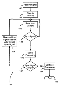
Fig. 15 is a flow diagram showing a sync signal detection method according
to an embodiment of the invention. The method 180 begins at step 182 when a
signal is
received. Portions of the received signal, or preferably digital samples
thereof, are stored in
a memory at step 184. At step 186, the samples are read from the memory by a
sync
signal detector. The sync signal detector then determines at step 188, through
a
correlation or other comparison process between the received signal and the
known sync
signal, whether or not a current portion of the received signal is the sync
signal. As
described above, a result of a correlation may be compared with a threshold to
determine
whether or not the sync signal has been detected. If the sync signal is not
detected in the
received signal, then step 186 is repeated. Where a sync signal is of a length
that is
greater than a portion of the received signal stored in a single memory
location, then the
sync signal detector may either read more than one location before performing
the above
comparison or sequentially compare the result of each memory read operation to
a portion
of the sync signal.
When the sync signal detector detects the sync signal at step 188, the
receiver is synchronized and the method proceeds at step 190 with further
processing of
the received signal. Step 190 is analogous to the receiver decode state
described above.
After a further portion of the received signal has been processed, a
determination of
whether or not the detected sync signal is an invalid sync signal may be made,
at step 192.
For example, a frame head portion of the received signal may be decoded and a
CRC
performed on the decoded data, as described above. If the decoded data does
not pass
the CRC, then the detected sync signal may be declared invalid.
If the sync signal is not declared invalid, then processing of the received
-25-
CA 02363930 2001-11-27
signal continues at steps 194 until an entire signal to be processed based on
the detected
sync signal, an entire frame of data for example, is processed. Once a
negative
determination is made at step 192, such that processing of a received signal
proceeds at
step 194, the sync signal detection method is complete and ends at step 196.
If the sync
signal is declared invalid, then the processing started at step 190 is
discontinued and the
sync signal detector resumes sync signal search operations at a point of the
received
signal just after the start of the previously detected invalid sync signal.
It should be apparent that the processing at steps 190 and 194 may be
similar or different. For example, if a sync signal is declared invalid based
on a BER or
SER, then step 194 may be a continuation of the processing that began at step
190.
Therefore, in the event that a detected sync signal is declared invalid, the
method 180 may
include a further step (not shown) of discontinuing processing of the received
signal.
Alternatively, if step 190 is frame head processing as described above, then
step 194 may
represent processing of frame data, such that when a sync signal is determined
to be
invalid, further processing of the received signal would not be executed. In
this latter
example, processing at step 190 is completed, and if a positive determination
is made at
step 192 is made then the further processing at step 194 is not executed, such
that there
may not necessarily be a step of discontinuing processing operations in all
embodiments of
the invention.
Although described primarily in the context of a particular receiver
architecture, the invention may be applied to virtually any communication
device in which
sync pattern detection is required. Wireless modems such as those disclosed in
United
States Patent 5,619,531, titled "Wireless Radio Modem with Minimal Interdevice
RF
-26-
CA 02363930 2001-11-27
Interference", issued on April 8, 1997, and United States Patent 5,764,693,
titled "Wireless
Radio Modem with Minimal Inter-Device RF Interference", issued on June 9,
1998, both
assigned to the assignee of the instant invention, represent types of
communication
devices in which the invention may be implemented. Many conventional wired
modems
also require sync pattern detection and therefore would be suitable for
application of the
invention.
In further preferred embodiments, the invention may be configured to operate
in conjunction with mobile communication devices, such as those disclosed in
United
States Patent No. 6,278,442, issued on August 21, 2001, and entitled "Hand-
Held
Electronic Device With a Keyboard Optimized for Use With the Thumbs". Other
systems
and devices in which the invention may be implemented include, but are not
limited to,
further fixed or mobile communication systems, hand-held communication
devices,
personal digital assistants (PDAs) with communication functions, cellular
telephones and
one-way or two-way pagers.
It will be appreciated that the above description relates to preferred
embodiments by way of example only. Many other variations of the invention
will be
obvious to those knowledgeable in the field, and such obvious variations are
within the
scope of the invention as described and claimed, whether or not expressly
described.
For example, the receiver 120 represents an illustrative embodiment of
instant invention. Practical implementation of the invention is in no way
restricted thereto.
The invention is applicable to both wired and wireless receivers, which may or
may not
include all of the functional blocks shown in Fig. 14. Similarly, receivers or
communication
devices in which the invention is implemented may also include further
functions and
-27-
CA 02363930 2001-11-27
components in addition to those disclosed above. In many contemplated
embodiments, a
receiver embodying sync pattern detection in accordance with the invention
would be a part
of a two-way communication device which would also include a transmitter.
_28_