Note: Descriptions are shown in the official language in which they were submitted.
03i14i2001 10:42 BLANK ROME COMISKY RND MCCRULEY -~
111420*0Id15Hts1'~d.5.5d51.541 Nu.~rd~ W~ou~
. , Pcr~uso o. ~ -0~2 5 t_ ~_
IPEA,/~S 12 JAN 2001
MODULAR PLUG CONNECTOR
AND IMPROVED RECEPTACLE THEREFOR
BACKGROUND OF THE INVENTION
1. Field of the Invention .
This invention relates to a multiple contact electrical connector, and in
particular to an improved High Speed Serial Oata Connector (HSSDC)
system made up of a modular plug and a receptacle having a polarization slot
. . ,,
-- ~ and a ferrite block filter.
2. ~cription of Related Art
The HSSDC system was developed to carry data over Ethernet
connections at full duplex rates of up to four Gigabits per second, over
extended cable lengths of up to ten kilometers_ Although not yet subject to a
formal IEEE standard, the IEEE draft proposal calls for eight signal lines
and,
in the case of extended length cable connections, an equalizer board
connected between the contacts of the plug connector and corresponding
' contacts of the cable.
In general, the HSSDC connector design is similar to other network
cable connector designs, but the presence of an equalizer board in the plug
connector, and the relative high data rates of the proposed HSSDC standard,
present a number of new problems. Although the problems are of particular
concern with respect to HSSDC connectors, however, those skilled in the art
will appreciate that the solutions to the problems may also have applicablllty
to other types of connectors, and in particular to other high speed multiple
contact data cable connectors.
.-,
S
~~I~;,J~r:.L v.G1.:~T
CA 02363950 2001-08-22
CA 02363950 2001-08-22
WO 00/51206 PCT/LTS00/02516
The first problem is the difficulty in assembling the contacts of the plug
connector to the equalizer board. Currently, both the connector contacts and
cable conductors must be soldered to the equalizer board before placement
of the entire assembly in the connector housing. As a result, special handling
of the cable and board is required, greatly complicating the manufacturing
process. While modular designs, including modular designs utilizing
solderless contact arrangements, have previously been proposed, the prior
designs have either pre-positioned the connector contacts in the module, as
is common in the case of RJ contacts, or provided a separate circuit board
module for various filter components, as in the case of SCSI or RJ
connectors. Neither of these two solutions is suitable for use in an HSSDC
connector system because of the configuration of the contacts which, unlike
RJ contacts, extend generally horizontally from the equalizer board, leaving
them vulnerable to damage during assembly, and because of the design of
the connector housing which, as a result of the high data rates, must
completely enclose the equalizer board, thereby making post assembly
termination of the cable to the circuit board impractical.
The second problem is that current assembly techniques require, in the
case of connectors that do not include an equalizer board, termination of the
connector contacts directly to the cable contacts before insertion into the
connector, which requires a separate assembly line. Even if a conventional
modular design could be used for such connectors, the problem would remain
that separate assembly procedures or different modules are required for
equalized and non-equalized connectors.
The third problem is the problem of polarization of the HSSDC system.
Because of the wide variety of devices that could use HSSDC type
connections, it is possible that devices could be cross-connected. It would
thus be desirable to include a way to prevent otherwise identical HSSDC
plugs from being plugged into the same receptacle.
2
CA 02363950 2001-08-22
WO 00/51206 PCT/US00/02516
Finally, the fourth problem involves the general problem of shielding
and filtering the contacts. While the HSSDC cable, plug, and receptacle are
all shielded against radio frequency (RF) interference, the currently proposed
connector design makes no allowance for filtering out spurious signals that
might result from electro-magnetic interference (EMI), which can be
significant due to the lengths of cable involved. Because of the unique
configuration of the HSSDC system connectors, the advantages of placing an
EMI filter within the HSSDC format connector have not previously been
recognized, even though EMI filter arrangements are well known in the
context of RJ, SCSI, and other less well-shielded cable/connector systems.
In addition, conventional filtering arrangements often add significantly to
the
cost of assembly because of the small size of the filters and the need to
terminate them to individual contacts.
SUMMARY OF THE INVENTION
It is accordingly a first objective of the invention to provide a high
speed connector system including a plug connector made up of a housing, a
plurality of contacts, and a circuit board connected to the contacts, in which
the circuit board and contacts may be connected to each other and
assembled to the connector using a modular design that does not require any
pre-soldering or pre-termination of the contacts to the equalizer board.
It is a second objective of the invention to provide a high speed
connector arrangement having a modular snap-together design that permits
the printed circuit board to be replaced, so that the same connector plug
housing can be used for applications that require equalization circuitry and
also for applications that do not require equalization circuitry.
It is a third objective of the invention to provide an HSSDC connector
system that includes EMI filtering and polarization features that allow plugs
to
be keyed to specific receptacles.
3
CA 02363950 2001-08-22
WO 00/51206 PCT/US00/02516
These objectives are achieved, in accordance with the principles of a
preferred embodiment of the invention, by providing an electrical plug
connector that includes two separate modules, one of which is an electrical
contact module that plugs into the housing, and the other of which is a board
that is also latched in the housing upon insertion of the board, the contacts
of
the electrical contact module being arranged to engage terminals of the
circuit
board upon insertion of the respective modules into the connector housing.
In an especially preferred embodiment of the invention, the plug
connector housing, contact module, and circuit board include first
complementary interengaging structures arranged to guide the contact
module and circuit board into their final positions in the housing, second
complementary interengaging structures arranged to latch the contact module
in its final position, and third complementary interengaging structures
arranged to latch the circuit board in its final position. The first
interengaging
structures preferably include a track extending along a sidewall of the
housing, and a rib extending laterally from the contact module and arranged
to fit within the track, while the second interengaging structures preferably
include a latch arm on the housing extending rearwardly relative to the
direction of insertion of the contact module into the housing, the latch arm
on
the housing having a downwardly extending projection, and a notch at a
trailing side of the rib extending laterally from the contact module, the
projection extending into the notch to latch the contact module in its final
position. The third interengaging structures preferably include a forwardly
extending latch arm on the housing, the latch arm of the third interengaging
structures including a projection extending laterally into the path of
insertion of
the contact module into the housing, and a notch in a side of the circuit
board,
the projection entering the notch to latch the circuit board into the housing
following latching of the contact module into the housing, at which time
contacts of the contact module engage terminals on the circuit board to
complete interconnection of the contacts with circuitry on the circuit board.
4
CA 02363950 2001-08-22
WO 00/51206 PCT/US00/02516
According to the preferred embodiment of the invention, the inclusion
of complementary interengaging structures for guiding and latching both the
contact module and the circuit board allows the connector to be completed by
simply snapping the various parts together. Furthermore, the modular design
of the preferred plug connector has the advantage that, if an equalization
circuit is not required for a particular connector implementation, the printed
circuit board having equalization circuitry can simply be replaced by a
printed
circuit board with traces that directly connect terminals on one side of the
board with terminals on the other side of the board, without having to change
the connector assembly procedure.
The objectives of the invention are further achieved, in accordance
with the preferred embodiment of the invention, by including polarizing
structures on the plug, and corresponding slots in the receptacle, the
dimensions of the respective plug structures and receptacle slots serving to
key the plug to the receptacle.
Finally, the objectives of the invention are also further achieved in
accordance with the preferred embodiment of the invention by including in the
receptacle structures that allows a filter block to be easily snapped into the
receptacle housing, the receptacle contacts being inserted through an
opening in the filter block so that the filter block surrounds the receptacle
contacts and thereby provides EMI filtering.
Although the illustrated connector is an HSSDC connector, and some
of the features of the invention involve considerations unique to HSSDC
connectors, those skilled in the art will appreciate that other features of
the
invention, such as the modular construction, may have wider applicability, and
in particular applicability to high speed data connectors other than those
specifically described in the HSSDC draft protocol and previous HSSDC
connector proposals.
5
CA 02363950 2001-08-22
WO 00/51206 PCT/US00/02516
BRIEF DESCRIPTION OF THE DRAWINGS
Fig. 1 is an isometric view of various parts of an HSSDC plug assembly
constructed in accordance with the principles of a preferred embodiment of
the invention.
Fig. 2 is a side view of the plug assembly parts illustrated in Fig. 1.
Fig. 3 is an isometric view of the plug assembly parts illustrated in Fig.
1, showing an intermediate step during assembly of the illustrated parts.
Fig. 4 is an isometric view of the plug assembly parts illustrated in Fig.
1, following assembly.
Fig. 5 is a cross-sectional side view of the assembly illustrated in Fig.
4.
Fig. 6 is an isometric view showing the assembly of Figs. 4 and 5
following installation of one-half of a metal shield.
Fig. 7 is an isometric view showing the assembly of Figs. 4 and 5,
following addition of the second shield half.
Figs. 8 and 9 are isometric views showing a completed version of the
connector illustrated in Figs. 1-7.
Fig. 10 is an isometric view showing various parts of an HSSDC
receptacle constructed in accordance with the principles of a preferred
embodiment of the invention.
Fig. 11 is an isometric view showing the receptacle body of Fig. 10
together with a shield.
6
CA 02363950 2001-08-22
WO 00/51206 PCT/US00/02516
Fig. 12 is an isometric view showing the receptacle of Fig. 11, following
assembly of the shield to the receptacle body.
Fig. 13 is a second isometric view of the assembled receptacle of Fig.
12.
Fig. 14 is a cross-sectional side view of the assembled receptacle of
Figs. 12 and 13.
Fig. 15 is an isometric view of a variation of the receptacle of Figs.
10-14.
Fig. 16 is an isometric view of an arrangement for shielding a printed
circuit board for use in a plug connector of the type illustrated in Figs. 1-
9.
DETAILED DESCRIPTION OF THE PREFERRED EMBODIMENTS
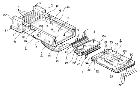
As illustrated in Figs. 1-5, the high speed connector plug of the
preferred embodiment of the invention includes an insulating housing
member 1, a contact module 2, and a printed circuit board 3. Insulating
housing member 1 may be made of molded plastic or any other suitable
dielectric or electrically insulating material, and includes a forward section
4
for insertion into a corresponding receptacle and rear section 4' in which the
contact module 2 and printed circuit board 3 are positioned.
Forward section 4 features a plurality of contact positioning slots 5 for
receiving forward mating portions 10 of a plurality of contacts 7, and a pair
of
laterally extending keys 8 which serve to prevent improper insertion of the
plug into the receptacle illustrated in Figs. 10-15. As illustrated in Fig. 5,
an
inwardly extending shelf 5' extends into slots 5 for supporting forward
extensions 9 of the contacts. The rear termination sections 11 of the contacts
7 are also curved to facilitate termination to the printed circuit board 3.
7
03i14i2001 10:42 HLRNK ROME COMISKY RND MCCAULEY ~ 1114~d»bbl5t~~~~~ 4
n
1PE.~ _
The rear section 4' of the connector housing member 1 is defined by a
horizontal planar section 12 from which extends side walls 13. Each of the
side walls 13 includes a guide track or slot 14 formed in its inner surface
and
open at the rear. Guide tracks of slots 14 extend horizontally the length of
the
respective side walls. Projecting forwardly from side walls 13 and rearwardly
from side walls 15 of front section 4 are respective latch arms 16 and 17
which extend into a space between the respective side walls 13 and 15, and
which include at their ends respective inwardly extending projections 18 and
downwardly extending projections 19 for latching the printed circuit board 3
and contact module 2 in the main housing member 1, as will be described
below.
Also Included on the main housing member 1 are projections 20 that
! extend from the outer surface of side walls 13 for securing a shield member,
and a latch arm 21 that engages a corresponding opening in the receptacle to
latch the plug in the receptacle in known fashion.
The contact module 2 is made up of an insulating housing 22 formed
from a plastic or other dielectric material into which the contacts 7 may, for
example, be insert molded, or which may be made up of two parts secured
i
together to capture the contacts therebetween to form a sub-assembly which
allows the contacts to be handled as a unit. Contact module housing 22
includes a planar extension 23 having a bevelled surface 24 far receiving the
edge of printed circuit board 3 and positioning one side of the circuit board
so
that terminals 29 engage rear termination sections 11 as is best shown in
Figs. 1 and 2. Terminals 29 are illustrated in dashed lines in Fig. 1 to
indicate
that they are on the side of the circuit board that faces termination sections
11, as illustrated in Fig. 2.
i
Projecting laterally from the sides of housing 22 are ribs 25, which are
arranged to fit within guide tracks or slots 14 on the inner surface of side
walls
13 in order to guide the contact module as it is being pushed into the housing
8
y~.i.W wJ~.J V~~_...~ ~,
CA 02363950 2001-08-22
03~14~2001 10:42 BLHNK ROME COM1SKY RND MC:C:HULtY -~
1114~d~1~1~15tiiil'fd.5.5b51.541 Nu. d7 order
. TIUS o ~ l ~ 2 5 .1_ ~_ .
S L~.JA~J 2001
member 1. The trailing ends of ribs 25 includes a'notch 26 so that as the
contact assembly is inserted into the housing member 1, projections 18 of
latch arms 16 engage ribs 25, causing latch arms 16 to be pushed outwardly
and allowing the contact module to be pushed past latch arms 16, the notch
26 presenting no obstacle to continued movement of the contact module into
the housing member i . As the contact module is pushed further into the
housing member, projections 19 of latch arms 17 engage ribs 25, causing
latch arms 17 to be moved upwardly in order to permit ribs 25 to clear the
projections until the projections reach notches 26, at which time the
projections enter the notches and latch the contact module into the housing
member. In order to facilitate movement of ribs 25 past the downwardly
extending projections 17 and 19, the leading edges of ribs 25 may be
I
__ ' i bevelled.
Circuit board 3 is a planar member Z7 having a rectangular shape on
which is situated circuit elements 28, which may be in the form either of
equalization circuitry or simply traces extending directly from terminals 29
at
the front of the board, which are engaged by the contacts, to terminals 30 at
the rear of the board, to which are connected by any suitable method the
conductors 31 of a cable. For purposes of the invention, the configuration of
circuitry or traces on the board is entirely conventional and therefore is
only
depicted in schematic fashion. As indicated above, if equalization circuitry
is
not required, the illustrated board having equalization may be replaced by a
board in which traces directly connect the terminals 29 and 30, allowing the
same modular design to be used for connectors with and without the
equalization ion circuitry.
As illustrated in Fig 16, board 3 may also be replaced by a board 3'
that is surrounded by a shielding or filtering element, such as a ferrite
block
65, the shieldinglfiltering element and/or the circuit board being modified as
necessary to fit within the connector housing, for example by including rib-
like
structures 66 on the shielding or filtering element.
9
CA 02363950 2001-08-22
CA 02363950 2001-08-22
WO 00/51206 PCT/US00/02516
The lateral edges of circuit board 3 include notches 32 which are
arranged such that, after the contact module has been latched into housing
member 1, and the circuit board has been pushed into the housing member
by inserting the lateral edges of the circuit board into guide tracks or slots
14,
the inwardly extending portions 18 of latch arms 16 clear section 33 of the
circuit board before extending into notches 32 in order to latch the circuit
board in the connector. To optimize use of space in the housing member,
notches 34 may be included at the front of the circuit board so that the front
edge of the circuit board can be pushed all the way to the contact module
without interfering with downwardly extending projections 19 of latch arms 17
As a result of the above-described latch and guide track structure,
assembly of the contacts 7 and circuit board 3 to the connector housing
member 1 simply involves pushing contact module 2 into the housing member
until the contact module snaps into place and is held by latch arms 17, and
then pushing printed circuit board 3, to which the cable has been pre-
terminated by any suitable termination method such as soldering, into the
connector housing member until it snaps Into place and is held by latch arms
16, at which point rear termination sections 11 of contacts 7 will engage
terminals 29 at the front of the board.
Once the contact module 2 and circuit board 3 have been assembled
to main housing 1, the connector is enclosed within a shield which may, as
illustrated in Figs. 6 and 7, include a lower shield half 35 and upper shield
half
36. Lower shield half 35 includes openings 37 for receiving projections 20 of
housing 1, and openings 38 for receiving inwardly extending latching
projections 39 of upper shield half 36, the upper and lower shield halves 35
and 36 overlapping to provide a continuous shielding structure. The structure
formed by shield halves 35 and 36 is then enclosed within an insulating outer
housing member 60, illustrated in Figs. 8 and 9, to ensure that the connector
can be safely handled by the user, a portion of shield half 36 being exposed
so that corresponding elements of the receptacle can engage it and provide
CA 02363950 2001-08-22
WO 00/51206 PCT/US00/02516
shielding continuity when the illustrated plug connector is inserted into a
receptacle.
Turning to Figs. 10-15, the receptacle corresponding the to plug of
Figs. 1-9 includes an electrically insulating receptacle main housing 40
having
an opening 41 receive the plug body 1, including an upper section 41' shaped
to receive the latch 21, and into which extends mating portions 42 of contacts
43. Contacts 43 are in Fig. !0 as being joined together by carrier element 44
but, as those skilled in the art will appreciate, carrier element 44 is
removed
following installation of the contacts in the insulating housing 40. Although
the tails 45 of the contacts are illustrated in Figs. 12 and 14 as being
surface
mount contact tails, it will also be appreciated by those skilled in the art
that
the contact tails may also extend downwardly in order to be inserted into
openings in a circuit board or card in the fashion of conventional PCB tails.
Receptacle main housing 40 includes board locks 46, openings 47 for
permitting passage of contacts 43 from the rear of the housing into opening
41, and various other openings, slots, and other conventional features, not
described in detail herein, for supporting the shield 48 and for supporting
the
contacts 43 within the opening 41.
As described above, the preferred plug connector includes polarizing
features in the form of keys arranged to permit individual plugs to be keyed
to a specific connector. Receptacle main housing 40 is thus arranged to
include polarizing slots 49 extending from the upper corners of the opening,
which are shaped and dimensioned to receive polarizing keys 8 of a
corresponding plug connector, if properly oriented during insertion. Those
skilled in the art will appreciate that while only two structures and two
keying
slots are shown, the number of the keying structures and slots may by varied
to provide multiple key combinations as necessary.
11
CA 02363950 2001-08-22
03i14i2001 10:42 HLRNK RDME COMISKY RND MCCRULEY ~ 1114~t~~~1~1~~~~~~~1 ~l~ ~
. o
..
>PFAIUS ~.2.~,~~ 2oai
Inclusion of an EMI filter in the receptacle main housing 40 is
accomplished, in the preferred embodiment of the invention, by including an
opening 50 in the lower surface 51 at the rear of the housing and two
downwardly extending latch amps 52 having at their lower distal ends inwardly
extending projections 53. Opening 50 extends transverse to the direction of
contact insertion across the entire width of the contact assembly. Latch arms
52 are arranged to engage corrosponding notches 54 in a filter block 55
inserted through opening 50 into the connector prior to mounting of the
' contacts, and thereby latch the filter block into the connector. Filter
block 55
includes an opening 56 through which the contacts may be inserted, and may
be in the form of a ferrite block, a monolithic filter containing both
inductive
and capacitive elements, or any other type of EMI filter configuration through
__ ~ which the contacts can be inserted and which can be latched into the
receptacle housing before insertion of the contacts.
The shield 48 shown in Figs. 11-15 is entirely conventional, except for
the presence of the polarizing openings 57 corresponding to slots 49 in the
main housing 40. Included in shield 48 are ground tabs 58 which extend into
opening 41 for engaging the exposed portion of plug connector shield 36 and
ground tabs 59 for engaging grounded sections of a panel or device in which
the connector is mounted, as well as ground tabs 60 for insertion into
' openings in a circuit board or card on which the receptacle is mounted.
Shield 48 also includes a rear panel fit which folds over the back of the
receptacle housing and is latched, for example by inwardly extending
horizontal sections 62 having tines 63, to slots 64 in the receptacle housing
in
order tv complete assembly.
The receptacle illustrated in Fig. 15 is identical to that illustrated in
Figs. 10-14, except for the presence of light emitting diodes (LEDs) 70 at the
top left and right comers openings 41, which serve as visual indicators for
the
connector, and therefore the receptacle illustrated in Fig.lS has been
12
CA 02363950 2001-08-22
WO 00/51206 PCT/IJS00/02516
assigned the same reference numerals as the receptacle illustrated in Figs.
10-14, and will not be described further herein.
Having thus described preferred embodiments of the invention in
sufficient detail to enable those skilled in the art to make and use the
invention, it will nevertheless be appreciated that variations and
modifications
of the illustrated embodiment may be made without departing from the spirit
of the invention, for example by adapting the modular design of the preferred
plug connector, or the snap-in filter arrangement of the preferred receptacle,
to connector systems other than the illustrated HSSDC connector system,
and it is intended that the invention not be limited by the above description
or
accompanying drawings, but that it be defined solely in accordance with the
appended claims.
13